 Yann Guidon / YGDES
The eXecute module of the TAP connects one domain with no RESET but 2 clocks, to another with one RESET and one clock. This makes it more complex than the others, as hinted by the end of the previous log The TAP's eXecute module.
- On the TAP side : CLK and /WR are two sources of clocking. CLK goes to the counter and the shift registers, /WR goes to the decode logic that takes the control at the end of each message.
CLK would not go very fast : 10MHz is reasonable (wires and other external effects would probably disturb the signal) and leaves 100ns between consecutive rising clock edges.
There MUST be a reasonable margin (100ns ?) between the last rising clock edge and the rising edge of /WR.
There is no RESET for several reasons :- The TAP must be able to work while the rest is in /RESET
- Adding a TAP-specific RESET pin would increase the external footprint and wiring
- The TAP can control /RESET from the inside
- Routing another /RESET could burden the rest of the chip
- By design, the TAP will work with the proper init sequence. (JTAG can also work without /RESET pin)
- The core has a free-running clock, as well as a HW /RESET external signal.
The clock could be as slow or fast as one wants, or even weird...
The /RESET can also be overtaken by the TAP.
.
.
For the communication with the FSM, the signal goes through two DFF as shown below :
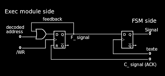
If the FSM clock is fast enough, the OR can be removed but... you're never too sure ! For example going from RESET to START triggers the reload of the instruction memory, which can take 4K cycles at least.
The first DFF triggers on /WR going up, which is the necessary condition to detect the end of the message, or else the "valid" address could be trigered by enough random data flowing through the shift register. The asynchronous RESET allows the crossing of clock domains, and the clearing always trails the setting by at least one FSM clock cycle, as delayed by the next DFF.
The DFF on the right also re-synchronises the input data so it is valid at the start of each FSM clock cycle. Otherwise the data could arrive late in the cycle and create race conditions and invalid boolean calculations.
.
.
Discussions
Become a Hackaday.io Member
Create an account to leave a comment. Already have an account? Log In.