 Luke Valenty
-
Introduction to Verilog and Combinatorial Logic
10/05/2017 at 05:00 • 11 commentsIntroduction
There are three primary methods for developing FPGA designs:
- Verilog
- VHDL
- Schematic Capture
The Hobbyist's Guide to FPGAs will focus on using Verilog to program FPGAs. Verilog and VHDL are both hardware description languages. They allow you to design digital logic circuits by describing them in their language. Verilog was chosen for this guide because it has an easier learning curve and is not quite as picky as VHDL is. There are some that would argue for using VHDL, and for good reason. VHDL has some powerful constructs that Verilog does not. For the average hobbyist, however, Verilog is the right choice and will provide a more pleasant entrance into the world of FPGAs.
Verilog
When designing any system, it is useful to be able to decompose the problem into smaller parts. Digital design is no different. In Verilog we have the concept of modules. A module is a self-contained design that communicates externally through ports. The ports on a module are input and output wires. You could think of a module as it's own standalone logic chip. When we are developing a new design, we start with a module.
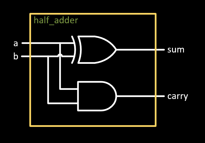
/*
 * Implements a simple 1-bit half-adder.
 */
module half_adder (
    input a,
    input b,
    output sum,
    output carry
);
    // sum is the xor of the two inputs
    assign sum = a ^ b;

    // carry is true only if both inputs are true
    assign carry = a & b;
endmodule
The above example is a reusable module that implements a half-adder. It's a nice and simple example that illustrates a few fundamental attributes of Verilog:
- All functionality is implemented within modules.
- Module ports have an associated direction.
- We can directly assign expressions to ports and wires.
- Expressions and comments in Verilog are very similar to expressions and comments in C, C++, and Java.
The assign statement performs a continuous assignment. It's not assigning a singular value to the left-hand side. Instead, it is assigning an expression to the left-hand side. If the value of any components of the expression changes, then the value of the left-hand side wire will change as well. The text of the Verilog translates directly into digital logic elements. If we designed the module as a schematic it might like similar to the one below:
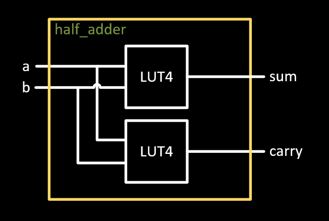
This is an accurate schematic of what the half adder module might look like if it were assembled with logic gates. FPGAs, despite their name, don't actually use logic gates. Instead they use much more powerful LUTs, or Look-Up Tables. In the actual FPGA implementation, the module would look more like the following diagram:
Instead of specific logic gates, the outputs of sum and carry are generated by the LUTs present in the FPGA fabric. The LUTs are programmed to behave like an XOR gate and an AND gate.
Modules can be reused in other modules. We can take our half adder and use it to create a full adder.
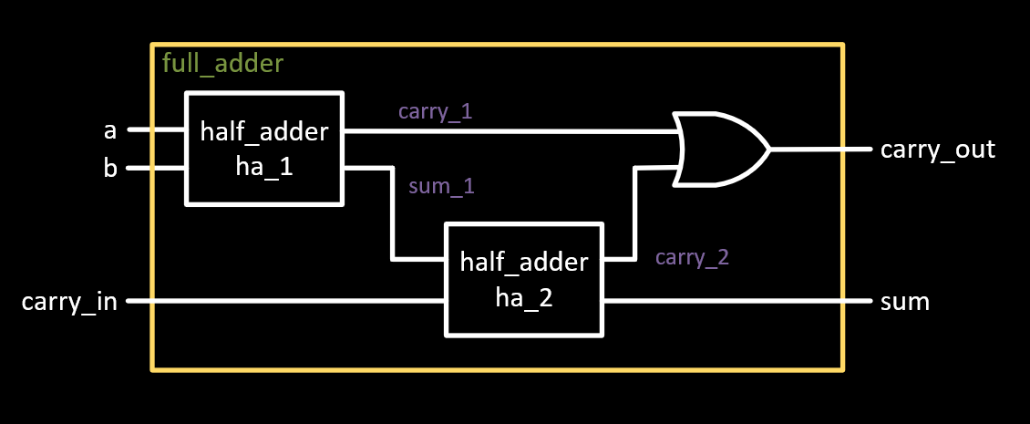
/*
 * Implements a 1-bit full-adder.
 */
module full_adder (
    input a,
    input b,
    input carry_in,
    output sum,
    output carry_out
);
    // carry outputs from half adders
    wire carry_1;
    wire carry_2;

    // intermediate sum from first half adder
    wire sum_1;

    // instantiate the first half adder
    half_adder ha_1 (
        .a(a),
        .b(b),
        .carry(carry_1),
        .sum(sum_1)
    );

    // instantiate the second half adder
    half_adder ha_2 (
        .a(sum_1),
        .b(carry_in),
        .carry(carry_2),
        .sum(sum)
    );

    // generate final carry out signal
    assign carry_out = carry_1 | carry_2;
endmodule
Here we see how modules can be reused and instantiated in another module. First the name of the module type is given, then the name of the instance, then a list of the ports and their connections. We also see that you can create wires internal to the module to connect components within the module.
If this were a schematic it would look like the following diagram:
Pretty neat, but given the amount of Verilog used to describe this simple design and the basic operation of addition we are building up to, you might be asking yourself: "Is this how much work I have to do just to add two numbers in Verilog!?" Luckily the answer is a resounding "No." Implementing an adder just happens to be a useful tool to dive into the most basic concepts of Verilog. Once we know how to implement a useful full-adder the hard way, we can cut to the chase and learn how to do it in a more logical way.
The next extension of this example is to enable larger than 1-bit numbers. This example will start to show the power of using a hardware description language vs. a schematic entry tool.
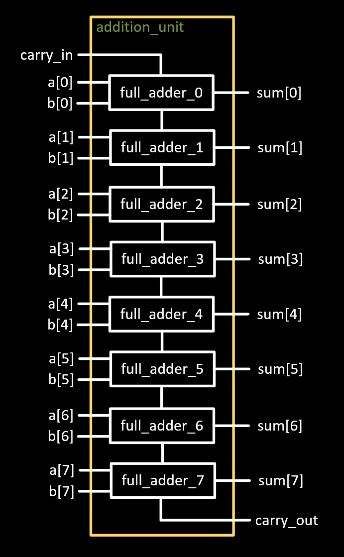
In order to add useful numbers we need several full-adders with a carry-chain connected between them. Let's start with the schematic representation first as the Verilog is going to start getting very interesting:
That's an eight-bit adder. It's pretty cool but it sure took longer for me to draw than I would like to admit. What if we want to expand it to larger or smaller sizes? It is not too convenient. There would be manual work involved in changing the number of bits in the adder. Hardware description languages like Verilog can do a much better job here. Verilog has the concept of module parameters and generate statements that will solve this problem very nicely.
/*
 * Implements a configuration addition unit.  Set the ADDER_WIDTH
 * parameter to the width in bits of the numbers you want to add.
 * If no ADDER_WIDTH is specified, then the default width of 8 bits
 * will be used.
 */
module addition_unit #(
    ADDER_WIDTH = 8
) (
    input carry_in,
    input [ADDER_WIDTH-1:0] a,
    input [ADDER_WIDTH-1:0] b,

    output [ADDER_WIDTH-1:0] sum,
    output carry_out
);
    // these are the wires that will connect the carry output
    // of one full adder to the carry input of the next full adder
    wire [ADDER_WIDTH:0] carry_chain;

    // use a generate block and for-loop to generate as many
    // full adders as we need.
    genvar i;
    generate
        for (i = 0; i < ADDER_WIDTH; i = i + 1) begin
            full_adder fa (
                .a(a[i]),
                .b(b[i]),
                .sum(sum[i]),
                .carry_in(carry_chain[i]),
                .carry_out(carry_chain[i + 1])
            );
        end
    endgenerate

    // connect carry_in and carry_out to the beginning and end
    // of the carry chain
    assign carry_chain[0] = carry_in;
    assign carry_out = carry_chain[ADDER_WIDTH];
endmodule
There are several new concepts introduced here:
- Module parameters! When you instantiate a module, you can also specify values for any of the module's parameters. This helps you to create reusable modules. In this example we use a parameter to specify the width in bits of the addition operation we are performing.
- Bit vectors. Instead of all wires and ports being one bit wide, we can create wires and ports with as many bits as we want using the bit-slice notation: [msb:lsb]. The indexes used in the bit-slice notation refer to the bit positions and are inclusive. For example: a bit-slice of "a[7:0]" is returning the lower 8 bits of "a".
- Generate blocks and for-loops. Generate blocks allow us to conditionally instantiate modules, assign statements, or always blocks; or even create multiple instances of the aforementioned constructs. In the above example we are using a for-loop in a generate block to instantiate as many full-adders as specified in the ADDER_WIDTH parameter.
A More Logical Approach to Addition
While addition served as an excellent way to describe how to create and use basic modules along with the more advanced concept of generation, this is is not how addition is performed in normal verilog code. There is a much easier way to implement an adder module:
module addition_unit #(
    ADDER_WIDTH = 8
) (
    input carry_in,
    input [ADDER_WIDTH-1:0] a,
    input [ADDER_WIDTH-1:0] b,

    output [ADDER_WIDTH-1:0] sum,
    output carry_out
);
    // create an internal sum that includes carry_out
    wire [ADDER_WIDTH:0] full_sum;

    // use the built-in addition operator
    assign full_sum = carry_in + a + b;

    assign carry_out = full_sum[ADDER_WIDTH];
endmodule
That's right, there is a built-in addition operator to Verilog. In fact, a standalone module would rarely be used like this in Verilog. It is more common for addition operators to be used in expressions just like bitwise logic operators are.
The FPGA synthesis tools know how to interpret the addition operator and will utilize optimized structures in the FPGA fabric to perform the addition operation. To further illustrate the power of Verilog over schematic entry, let's expand upon our adder concept. Let's create a simple arithmetic logic unit like one that might be found in a simple microcontroller.
module alu #(
    ALU_WIDTH = 8
) (
    // what type of operation should the ALU perform
    input [2:0] opcode,
    // input operands
    input [ALU_WIDTH-1:0] a,
    input [ALU_WIDTH-1:0] b,

    // operation output
    output reg [ALU_WIDTH-1:0] out
);
    // we want to use a combinatorial always block so we can use
    // a case statement to decide what to do.
    always @(*) begin
        case (opcode)
            0: out <= a + b;
            1: out <= a - b;
            2: out <= a & b;
            3: out <= a | b;
            4: out <= a ^ b;
            5: out <= ~a;
            6: out <= a << 1;
            7: out <= a >> 1;
        endcase
    end
endmodule
This is a very simple ALU. It is missing useful features like overflow and carry inputs, but I'll leave that as an exercise for the reader to. Now we are introduced to a very important concept in Verilog: the always block. An always block is a block of code that is "evaluated" every time a signal in its sensitivity list changes. In this example I used a * character to make the always block sensitive to all signals it uses.
Without having to write a large amount of code we have a basic arithmetic logic unit. We can add, subtract, perform boolean operations, and shift the input left and right. Not only is all the logic for those operations automatically inferred by the synthesis tools, the case statement will be interpreted as a 8:1 mux as well.
Conclusion
In a short amount of time this tutorial has taken the reader head-long into the fundamental features of Verilog for developing on FPGAs. I sincerely hope this was an enjoyable read. Stay-tuned, the next log will be a hands-on lab taking advantage of the concepts learned here and putting them to use on a hobbyist FPGA board.
To complete the upcoming lab on your own you can use use any of the TinyFPGA boards available at the TinyFPGA Tindie store. If you are deciding on which TinyFPGA to use, please read the user guides for the different boards at tinyfpga.com. The A-series boards need a bit more components to get up and running while the B-series boards are ready to go once plugged into USB.
You will also want a breadboard, some switches you can plug in, LEDs, and resistors for the switches and LEDs. More details about components required will be in the lab itself.
Until next time!
-
What are FPGAs?
10/02/2017 at 07:10 • 1 commentFPGAs and Microcontrollers
FPGA is an initialism for Field Programmable Gate Array. They are digital logic chips that can be programmed with new logic designs in the same way that microcontrollers can be programmed with new firmware. On a microcontroller, a program is a series of instructions the CPU executes one at a time. Each instruction takes time to execute, program memory to store, and may access locations in RAM.
Designs for FPGAs are different from programs in microcontrollers. The design defines a series of digital logic circuits, the connections, RAM and ROMs they may use, multipliers, etc. Each element of the design consumes a physical location of the FPGA. In a microcontroller instructions are executed one at a time. In an FPGA all elements of the design can be active at once. This makes FPGAs very powerful. In fact, an FPGA can implement a microcontroller in addition to custom logic.
Architecture
Inside many modern FPGAs there is an array of 4-input logic function generators, single bit storage elements, and other small bits of general purpose logic connected by a routing matrix. The image below is what a logic slice from the MachXO2 FPGA in the #TinyFPGA A-Series boards looks like.
MachXO2 FPGA Logic Slice. From the MachXO2 User Guide - http://www.latticesemi.com/view_document?document_id=38834
Rather than using individual 2-input logic gates, the LUT4 logic function generators or Look-Up Tables can generate any 4-bit logic function. The output of the logic generator can either be routed to another LUT4 elsewhere, or can be stored in the D Flip-Flop immediately connected to the output of the LUT4.
Many FPGA architectures group slices into larger elements. In the MachXO2 series from Lattice they are called PFUs, or Programmable Function Units. Since addition, subtraction, and comparison operators are so common, there is an optimized carry-chain between neighboring slices that allows for faster execution of such operations.
MachXO2 FPGA Programmable Function Unit. From the MachXO2 User Guide - http://www.latticesemi.com/view_document?document_id=38834
Between the PFUs is a routing matrix with many wires and switching matrices that allow for connections between PFUs and other components in the FPGA. In addition to the PFUs, FPGAs may contain other modules like RAMs, clocks, PLLs, non-volatile memory, and even hard-coded peripherals like SPI and i2c masters and slaves. The picture below is the basic layout of the MachXO2-1200 FPGA in the TinyFPGA A2 board.
MachXO2-1200 FPGA Top View. From the MachXO2 User Guide -http://www.latticesemi.com/view_document?document_id=38834
Programming
Every programmable element within an FPGA stores is programming locally. The LUT4 function generators for example contain 16-bits of information. The 4 bits of input can be interpreted as a numerical index into that information and the output is the value at that location. All of the routing programming contains storage bits that define how the design connects the various components. This configuration is stored in volatile storage elements. When the power goes off, they lose their state.
This means FPGAs need to be reprogrammed every time they power-on. Luckily there are automated mechanisms for FPGAs to load their configuration from an external flash memory, or even an internal flash memory on power-on.
In the #TinyFPGA A-Series this configuration flash is built into the FPGA itself. In the #TinyFPGA B-Series boards this configuration flash is on a separate SPI flash chip integrated on the board. Once a design is synthesized, it can be programmed onto the configuration flash on the board.
Developing for FPGAs
FPGAs come in chip packages that are difficult to integrate into hobbyist projects. Therefore there are development boards for FPGAs that contain the chip assembled on a PCB along with all the necessary support circuitry to operate the FPGA. The #TinyFPGA A-Series and #TinyFPGA B-Series boards are two such series of boards with differing capacities and capabilities. They are designed to be easy to integrate into existing hobbyist projects by plugging into breadboards. The low-cost of the boards allows them to be left in the project as a permanent component.
Designs for FPGAs are typically written using a hardware description language like Verilog or VHDL. However, there are also schematic entry tools that allow for graphical descriptions of digital logic circuits. The Lattice Diamond development environment for the MachXO2 FPGAs in the #TinyFPGA A-Series boards supports Verilog, VHDL, and schematic entry for developing designs. The iCECube2 development environment for the iCE40 FPGAs in the #TinyFPGA B-Series supports Verilog and VHDL, but it does not have a built-in schematic capture. However, there is an experimental graphical environment, icestudio, that may be used.
Uses for FPGAs
FPGAs can be used to solve a large variety of problems. They can act as a support or offload for a computer or microcontroller. Some examples:
- Input/Output Peripheral
- USB Device/Host
- SPI Slave/Master
- I2C Slave/Master
- GPIO
- UART
- Video Generator
- Keyboard Controller
- Physical Control and Interaction
- Precise Stepper Motor Control
- Servo Motor Control
- Sensor Reading
- Compute Acceleration
- High Speed Hash Functions
- Digital Signal Processing
- Neural Network Processing
- Graphics Acceleration
- Video Processing
- Audio Generation and Processing
These are just some examples of an FPGA being used to supplement a microcontroller. But an FPGA can be the central component of a project as well and utilize concepts from above:
- Homebrew Computer Designs
- Classic Computer Implementations
- Custom Microcontrollers and CPUs
- Esoteric CPUs
Another category small FPGA boards in particular can be used for is replacing components that are no longer available, hard to come by, or just not at your workbench at the moment:
- 74-series logic chips
- Microcontrollers
- Classic computer peripheral chips
- Classic CPUs (6502, z80, 8080, etc.)
This list is just a tiny glimpse into the possibilities afforded by FPGAs. They are an indispensable component that every maker can benefit from.
Now we have a basic idea of what FPGAs are and what they can do. The next steps are learning how to develop for them.
If you are interested in getting started with FPGAs I encourage you to take a look at the TinyFPGA Tindie Store for some low-cost options. Tutorials and labs in this series will utilize those FPGA boards.
- Input/Output Peripheral
The Hobbyists Guide to FPGAs
Follow this project to learn how to use FPGAs and incorporate them into your projects.
 MachXO2 FPGA Logic Slice. From the MachXO2 User Guide -
 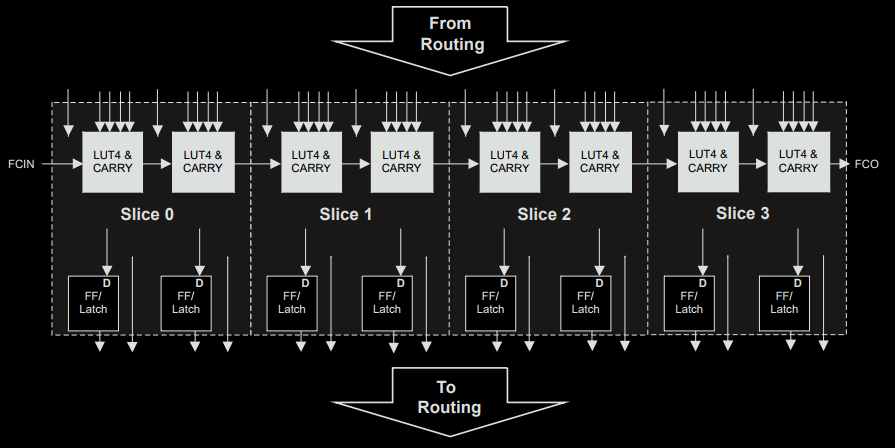 MachXO2 FPGA Programmable Function Unit. From the MachXO2 User Guide -
 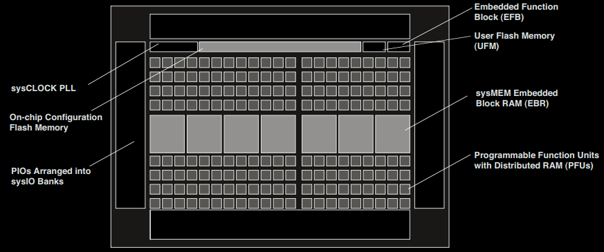 MachXO2-1200 FPGA Top View. From the MachXO2 User Guide -