 deʃhipu
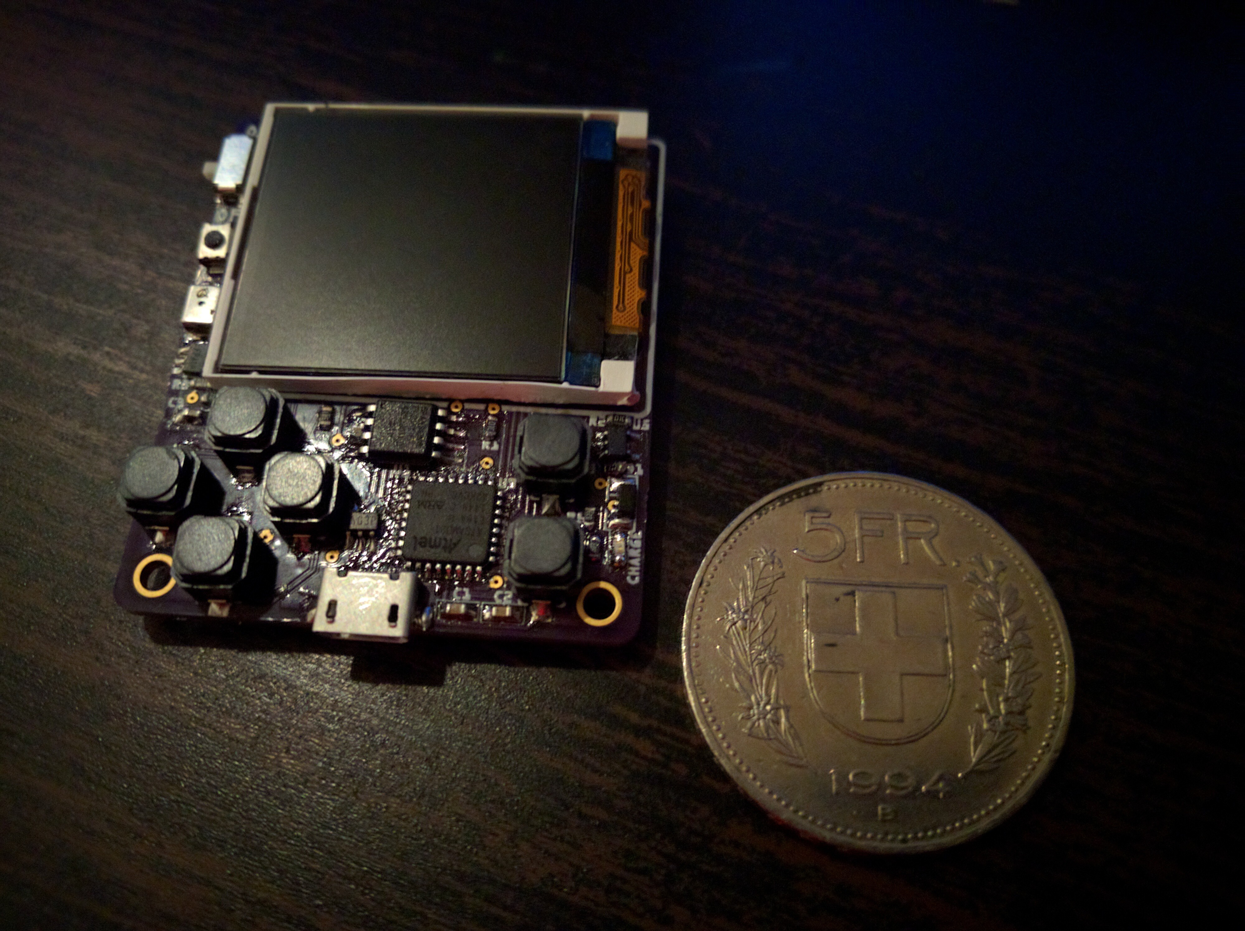
The PCBs for version 6 arrived about a week ago, but I didn't have time to work on it, between the day job and being sick. This evening I finally tested it properly:
The good things:
- moving the audio circuit was a good move, it's now completely out of reach of fingers, and I think it also seems a bit louder when the LOS is not obscured by hands,
- using straight switch instead of angled one for reset also works well — I can have a hole in the case (if I have a case) for pressing it with a pin,
- straight buttons are easier to solder,
- adding a CS pin made the displays all work consistently,
- moving the LDO away from the buttons also made it easier to solder.
There are still some rough edges, though, that I only found out after actually testing a physical prototype.
The bad things:
- the CS pin uses a via, and touching that via with your fingers makes the display stop updating — I need to route that trace on front side entirely,
- the charging LED still shines whenever USB is connected, even if the battery is disconnected — it does go off when the battery is fully charged, though,
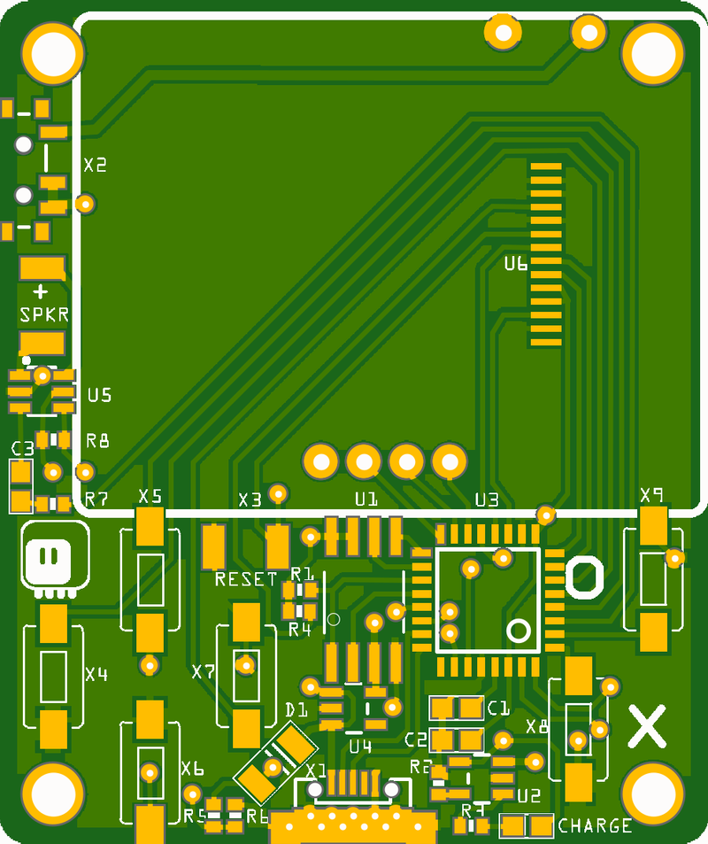
So I scrapped the version 7 which was basically just a cleanup of version 6 ready for ordering a larger number of them, and prepared version 8. I moved practically all parts around, including the microcontroller and the flash chip, but now:
- the reset button is next to the direction buttons, not on the edge of the pcb,
- all components, except for the audio circuit, are together in the middle of the board,
- the signals for audio and for the display are routed on one side without any vias,
- there are no parts under the fingers anymore,
- the top fire button got moved to the edge to make room for the parts, so now the layout looks more like gameboy,
- all the parts are better spaced and have shorter traces between them,
- there are more mounting holes (some are under the display, but with flat heads that could still be useful),
- I have broken out four unused pins on the back, for possible hacking,
- I moved the battery connector to the other side of the board, so it now matches the layout of Nokia phone (dumb) batteries.
I know I said that about the previous version, but this is really to be the last one I'm making (at least with this microcontroller and display) — if everything works, that is. I'm going to order this one at Aisler again, to see how they improved (and to get a stencil).
Discussions
Become a Hackaday.io Member
Create an account to leave a comment. Already have an account? Log In.
There shouldn't be a problem with a finger on CS. Do you drive it with a normal output port? Do you have the circuit diagram in PDF format? Couldn't open the fzz files and looks like the last version is 5 in your github repository.
Are you sure? yes | no
I don't want to push the changes before I have tested the PCB, so that people don't get surprises. But I added the schematic to the download files: https://cdn.hackaday.io/files/276291182079136/output.pdf
Are you sure? yes | no
The pin names are wrong at the display connector, but I assume it is ok. Maybe check if the CS pin is configured as push-pull and not open-drain or something like this. A finger shouldn't change it much. But you could try to add a small delay after pulling CS low, a finger could change the signal form a bit, which would be an indication that something is on the edge. I would measure the timings with a scope and verify that everything is within the spec of the display, like setup and hold times, max clock speed etc.
BTW, I don't see a via for the CS signal. In your circuit diagram it is pin 12, display CS. Isn't this the 4th pin on the top pin row, counting from right, because pin 1 is bottom right?
Are you sure? yes | no
Yes, because that's the new, redesigned pcb, without any vias on signal lines (and with cs and dc swapped, so that they don't cross).
Are you sure? yes | no
Oh, and the display indeed has wrong labels, because I edited a footprint for a different display to adapt it, and for some reason Fritzing didn't update the labels on the schematic graphic. I guess another bug.
Are you sure? yes | no
Regarding the problem with the via on the CS line: why not just tent your vias?
Are you sure? yes | no
Same reason why I keep the PCB size under 5cm — so that you can make it cheaply at any PCB fab out there. Also, it's more nitpicking now, because there would be a battery taped there anyways... So I just consider this practice.
Are you sure? yes | no