Ian Hanschen
-
IT'S ALLLIIIVEEEE!
03/30/2018 at 04:06 • 7 commentsWell I managed to snag an NX-4 control box off ebay for 100 bucks last week! It was a total pig in a poke (kind of like the LED tiles were) but it seems to work, at least enough to drive the displays! I have it showing test patterns and stuff now using it.
The wiring is now figured out for the cables, and it works like this:
(8 pin "out" connector -> 9 pin "in" connector)
1 - > 1 (+24V)
2 -> 6 (GND)
3 -> 7 (out data to display positive)
4 -> 3 (out clock to display negative)
5 -> 5 (in data from display positive)
6 -> 2 (out data to display negative)
7 -> 8 (out clock to display positive)
8 -> 4 (in data from display negative)
It appears the cable from the NX control box to the tile, and the cable between tiles is the same. I guess this would make sense.
Inside the NX control box proper is a huge 24V, 15A(!) power supply. It has an IEC receptacle on it, but unfortunately it is only for 240V operation. It will not run on 120V. The supply is extremely high quality and has a very small for this power level planar transformer inside and a PIC micro. It also has I^2C for some reason. I cannot use the existing supply so I am just hooking my bench supply up for now and running a single tile.
A quick scoping reveals the clock going to the display is 50MHz which is a bit higher than I was expecting but not too far out of the ordinary I guess. I initially didn't twist my pairs because I was lazy, and it resulted in it not working very well at all.
![]()
Holding the wires together with my finger seemed to make it work a lot better and I started to get actual data on the display! Interesting how the word "up" was showing up in green at the bottom there.
![]()
Finally, after doing it right and twisting the pairs, it seemed to be working properly.
![]()
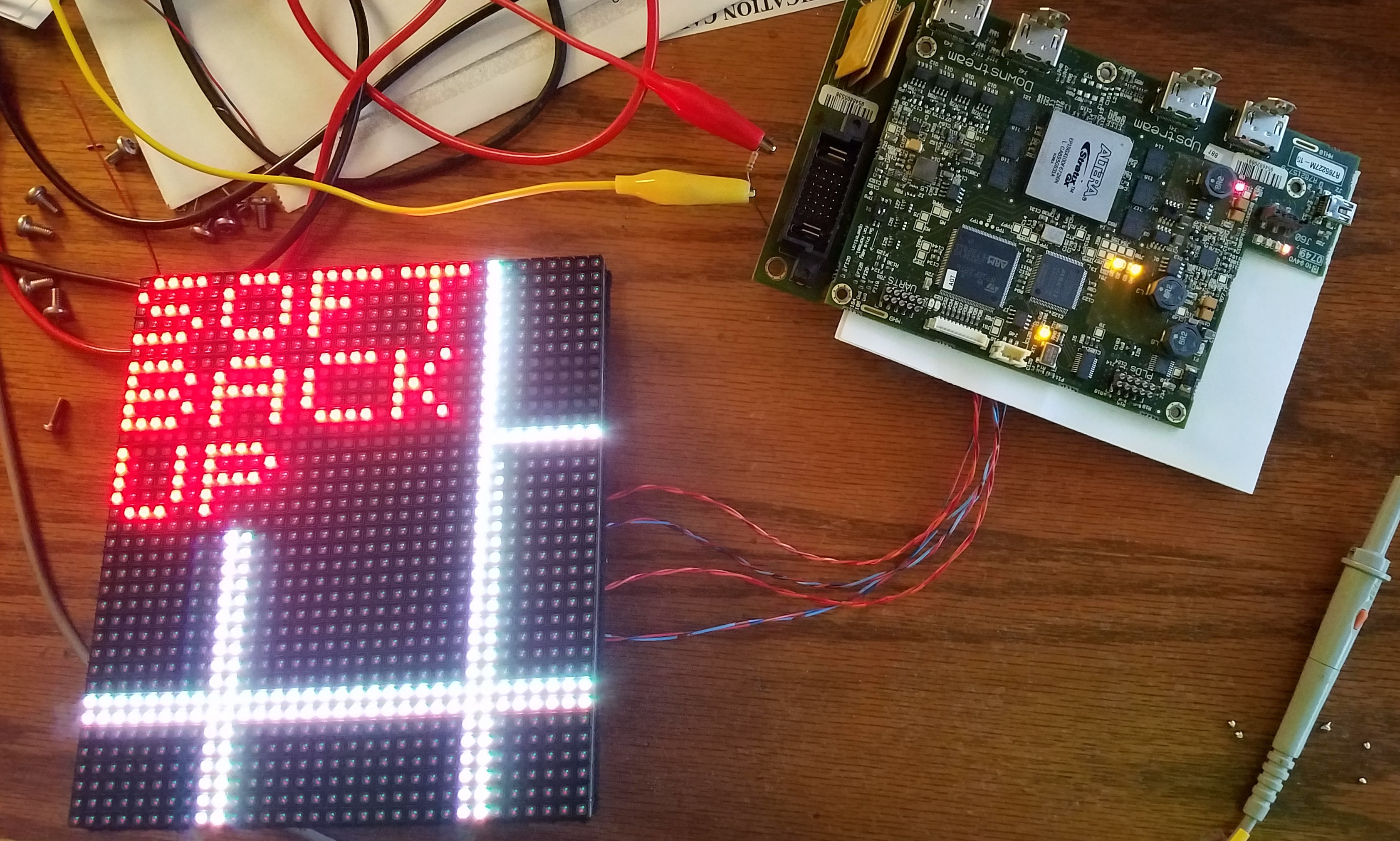
There's a two position dip switch on the board with the text "sw this way for normal operation" with an arrow. If both of the switches are in the down position, it will display a moving white grid pattern that marches down and to the right one row/column every 300ms or so. I assume this is so you can tell if you have arranged the tiles properly in the array and have not turned one or more of them.
If one switch is up and the other is down, you get the "soft back up" message with the marching row/column behind it. I am not sure what this means but it is probably documented in the manual.
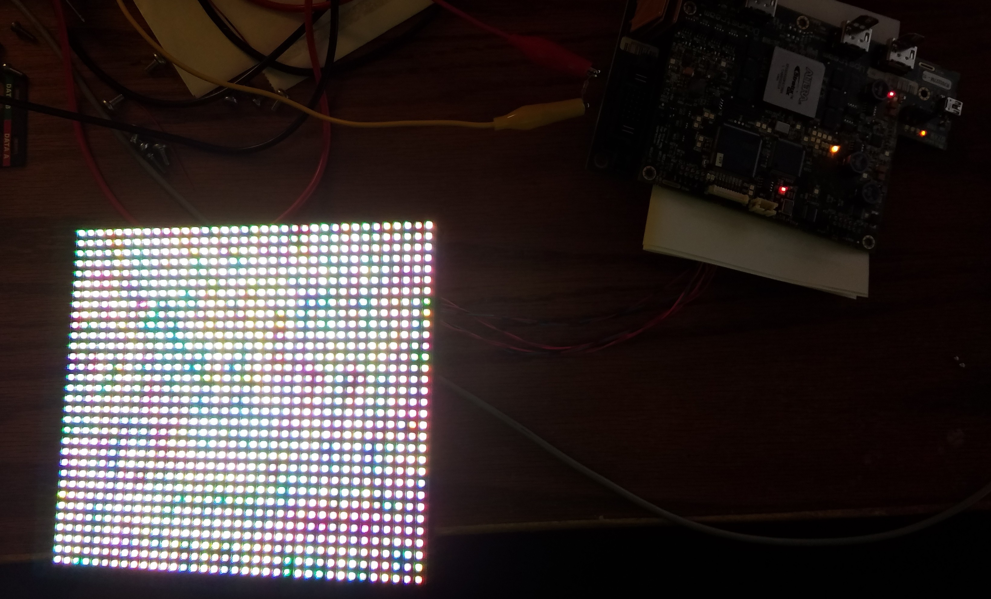
Clicking both up in the "normal" position, results in all LEDs glowing a dim grey, I suspect for LED testing or similar. On this panel all LEDs appear to light and with absolutely uniform brightness.
There's a ton of LEDs on the control PCB and they all flash various patterns. I am not sure what they mean but there's four LEDs near the connector to the indicator LEDs for the box which indicate status. One flashes yellow about once a second (sometimes it will flash twice in a pattern) and the other flashes orange 3-4x a second.
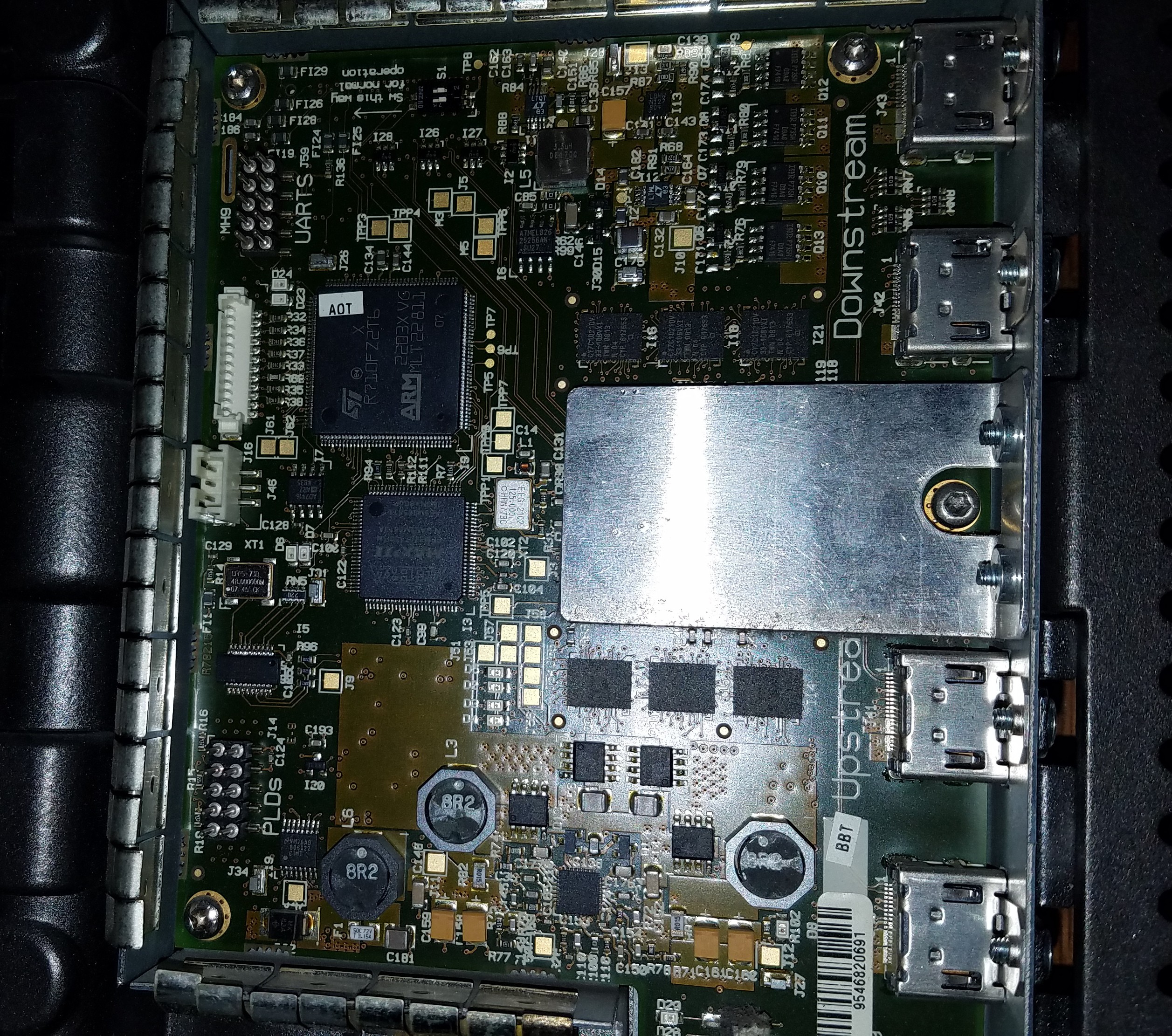
Hardware on the control board is pretty brute force. There's an ARM CPU, Stratix GX FPGA (with 8 serdes, two per HDMI connector to link the control boxes together as shown in the docs), 6 128Kbyte 15ns SRAMs, a maxii CPLD, and a bunch of power supplies.
On the bottom is a 4mbyte parallel flash ROM and a MAX232 RS232 transceiver. There is also a mini USB connected to the ARM, but I have not plugged anything into it yet. There are 3 big honking 9A 30V polyswitches to limit current to each string of three LED panels as well.That's about it for now, I just got this box today and had to do a quick play around to see if I could get it to light up one of the LED panels, and it did! I hope it isn't too tough to hook this up to an FPGA and do some heavy duty reverse engineering of their protocol now.
Finally, a crappy pic of the board inside the box.
![]()
-
A Slight Disaster and More Info
12/05/2017 at 11:12 • 4 commentsI decided to try and feed the display so more LFSR goodness, and I managed to get the link light to stay lit, and the fan kept spinning. Buoyed by this success, I kept at it and could keep the LED/fan on longer. Each time the FPGA was reset, the LEDs would flash on briefly with a different pattern too.
But, after awhile the status LED started doing a double flash. This means I blew away the main application firmware somehow. Whoops. Checking the rental install PDF, this means that the board is running on backup firmware. I will eventually desolder the flash on this board anyways for testing, and I will replace it with two .5mm FFC connectors to hook it up to my tester.
In the mean time, I will remove the flash from another board, bend pin 10 (/WE) up and reinstall, then solder /WE to 3.3V to prevent the flash getting blown away with subsequent poking. I should've done this from the start, but these things happen.
I was doing a bunch of poking around the barco website, and their "director toolset" is available for download. Inside the install file, I found all the various firmware images for what looks like every (or nearly so) LED product they make and have made. There's no registration or other requirements it seems and the installer is there for download.
https://www.barco.com/en/product/director-toolset
I used winzip to unpack the installer without running it.
In the installer it lives at: /install/install/installerdata/disk1/instdata/resource1.zip
in resource1.zip: /$IA_PROJECT_DIR$/directortoolset_2.08-win.zip
in the above zip: /flashfiles/
whew!
Inside was the firmware/software for these tiles. The FPGA bitstream and the microblaze code are separate files. There's a couple versions of each for the NX4 stuff. These appear to have a bit more metadata in them but otherwise look similar to the stuff found in the parallel flash.
The interesting files are named:
Nx firmware_ctrl 4.0.0.hwr (434K)
Nx firmware_mod 4.0.0.hwr (166K)
Nx program 4.0.0.swr (129K)
Nx program_backup 2.0.0.swr (57K)
Nx program_mod 4.1.0.swr (75K)
The documentation pdf that is on the director toolset link is also kind of interesting; it explains things like calibrating the display using a camera, manually, etc. as well as the kinds of diagnostic information available. These displays are also capable of gap compensation where it dims the pixels on the inside vs. the outside to make gaps less noticeable.. neat.
-
I^2C for Fun and Profit
12/03/2017 at 01:22 • 2 commentsAfter some messing around, I managed to capture the entire I^2C sequence on startup, and now have a complete log of what happens on the bus.
Looks like it initializes everything and then reads a bunch of the data out of the EEPROM on the LED board which isn't too surprising. Every 2 seconds, it reads the two temperature sensors. I will have a link below to the entire data log in human readable format. Here's some highlights, though, with my notes:
At the start, there's a bunch of small 1-4 byte reads out of the two EEPROMs, most likely reading version/model information.
START
DEVADD: 50 WRITE ACK
SUBADD: 0F ACK 10 ACKSTART
DEVADD: 50 READ ACK
SUBADD: 32 ACK 32 ACK 32 ACK 32 NACKSTOP
START
DEVADD: 50 WRITE ACK
SUBADD: 0F ACK 14 ACKSTART
DEVADD: 50 READ ACK
SUBADD: 00 ACK 12 NACKSTOP
START
DEVADD: 51 WRITE ACK
SUBADD: 01 ACK 00 ACKSTART
DEVADD: 51 READ ACK
SUBADD: 32 ACK 32 ACK 32 ACK 32 NACKSTOP
START
DEVADD: 51 WRITE ACK
SUBADD: 01 ACK 04 ACKSTART
DEVADD: 51 READ ACK
SUBADD: 00 ACK 05 NACKSTOP
If you know about I^2C, the above should be self-explainatory. If not, here's how a typical EEPROM read works: First, the start condition tells the chip a transmission is happening; then it sends the device address (50h is the control board's EEPROM, 51h is the display board's). The direction of the following command is sent (read or write) then the sub-address.
For the first transmission the address 0F10h is sent. To read from a location in the EEPROM, you first tell the chip you're going to write and specify an address, then repeat the start condition with read. This is kinda hacky IMO but it is how it works.
After this, the EEPROM will spit out 1 or more bytes. Your code has to ACK each byte except the last; at which point you NACK to tell the chip you're done with it, and finally end with a stop condition.
So right off the bat, they are reading locations 0F10h-0F13h from the control board EEPROM, then they read from 0F14h-0F15h.
They then read from the EEPROM on the LED board in a similar manner, except it's reading addresses 0100-0103h and then 0104h-0105h.
There's some more transfers from the two EEPROMs and then they initialize the light sensor:
START
DEVADD: 39 WRITE ACK
SUBADD: 80 ACK 03 ACKSTOP
START
DEVADD: 39 WRITE ACK
SUBADD: 81 ACK 00 ACKSTOP
Going by the datasheet for the TSL2560CL ( https://www.digikey.com/product-detail/en/ams/TSL2560CL/TSL2560CLTR-ND/3095174 )Device address 39h is the sensor, then they write 03h to register 00h which turns the chip on. Register 00h is the configuration register.
Next, they write 00h to register 01h. This is the "timing register". It sets the gain to 1x, and sets integration time to 13.7ms (the longest integration time available).
After this, the two temperature sensors are initialized:
START
DEVADD: 49 WRITE ACK
SUBADD: 01 ACK 00 ACKSTOP
START
DEVADD: 49 WRITE ACK
SUBADD: 05 ACK 00 ACKSTOP
START
DEVADD: 49 WRITE ACK
SUBADD: 02 ACK 4B ACK 00 ACKSTOP
START
DEVADD: 49 WRITE ACK
SUBADD: 03 ACK 55 ACK 00 ACKSTOP
START
DEVADD: 48 WRITE ACK
SUBADD: 01 ACK 00 ACKSTOP
START
DEVADD: 48 WRITE ACK
SUBADD: 05 ACK 00 ACKSTOP
START
DEVADD: 48 WRITE ACK
SUBADD: 02 ACK 4B ACK 00 ACKSTOP
START
DEVADD: 48 WRITE ACK
SUBADD: 03 ACK 55 ACK 00 ACKSTOP
Device addresses 48h and 49h are the two temperature sensors. Both are programmed identically. The meaning of the writes is:
01h 00h: Write 00h to register 01h- this is the configuration register. This selects temperature sensor 0 (the internal temperature sensor), clears the error queue, and turns the chip on.
05h 00h: Write 00h to register 05h- this is the secondary configuration register. It's simply zeroed out since this chip does not have the "conversion start" pin.
02h 4bh 00h: Writes 4b00h to register 02h- this sets the lower hysteresis trip point for overtemp. 4bh = 75C.
03h 55h 00h: Writes 5500h to register 03h- this sets the upper trip point for overtemp. 55h = 85C.
Interestingly the overtemp output pin is not used, yet they still set trip points for it. They periodically read the temperature manually to check it and the overtemp pin is not connected to anything as far as I can tell.
After this, there are more reads (a lot more reads) from the control EEPROM and it gets written to the SRAM. The LED board's EEPROM is barely used. Maybe the outside controller has to request calibration data? Maybe the calibration data is stored in the control EEPROM? I doubt this but I guess it is possible.
During the EEPROM read, it gets interrupted to perform a temperature read:
START
DEVADD: 48 WRITE ACK
SUBADD: 00 ACKSTOP
START
DEVADD: 48 READ ACK
SUBADD: 1A ACK C0 NACKSTOP
START
DEVADD: 49 WRITE ACK
SUBADD: 00 ACKSTOP
START
DEVADD: 49 READ ACK
SUBADD: 1C ACK 80 NACKSTOP
Basically what it is doing is reading register 00h. This is done by outputting a device address with write set, and then the sub address they wish to read (or write).
Then they do a device address + read, and get back 1AC0h (this is the 10 bit temperature, left shifted 6x). 1Ah = 26C. The second board's temp sensor is read in a similar manner and returns 1Ch which is 28C.
These temp reads are repeated every 2 seconds while power is on.
Anyways, here's the log I made.
http://blog.kevtris.org/blogfiles/iic.txt
Enjoy!
-
The Adventure Begins
12/02/2017 at 10:01 • 0 commentsWell, I have one of the modules connected up to my general purpose FPGA reverse engineering / ROM emulation rig. There's no ROM emulation yet but I can feed it arbitrary data and receive data from the display.
For testing, I sent it LFSR data (41 bit LFSR) at various speeds from 100KHz to 10MHz or so and so far nothing happened. This isn't too surprising I guess. It most likely has some kind of complex packet structure to turn the display on and configure it.
I also hooked the FPGA's programming pin up that reconfigures it so I can reboot the board without having to power it down and up again. This lets me catch anything that happens on startup. While I was soldering wires, I connected the I^2C bus to my board as well.
I will record the entire I^2C startup sequence (it's long and takes a few seconds) along with the data that comes back out of the chip on startup. There's 4mbytes of RAM which should be plenty for this application.
Eventually I want to replace the RAM/ROM on the board with an adapter for this emulator board and probe memory as it runs.
One interesting thing is if you reset the board, some random rows of LEDs will flash on and off quickly as the CPLD is sent the control signals. This doesn't happen from poweron, just if you reset the FPGA.
The data coming back from the display seems to be boring and so far not too interesting. It's the same data that it spits out of the output jack. It is a 10 bit repeating pattern: 1111111111111111_0001110101_0001110101_0001110101. If the data is interpreted such that the initial 0 is a start bit, the data becomes 0011_1010 with an extra "1" stop bit. This is ASCII for the backslash (\) character. I guess the data format might be basically RS-232 like in nature but synchronous instead of asynchronous.
Changing the input clock over the entire 10KHz to 10MHz range resulted in the same exact synchronous data stream coming out. Maybe the display is looking for text/data strings? That'd be pretty interesting if so (and I suspect they will be present in the parallel flash). It most likely is packetized format, and there will be commands to turn it on, check the calibration, read the temp sensors, etc. As it is, the I^2C is not accessed again after startup so it is obviously sitting and waiting for commands before it starts doing stuff (tm). If it is packetized it probably is checking for a hash/checksum too and it will not accept the data unless this is present.
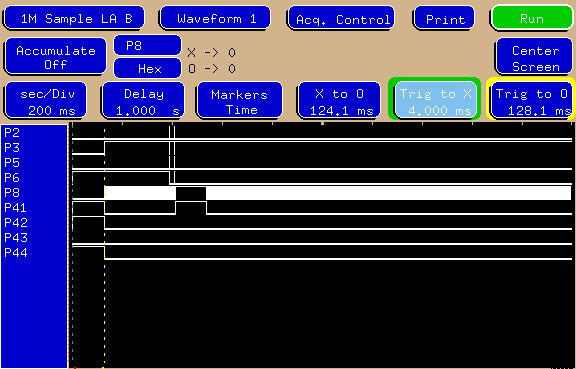
Here's a quick dump from signaltap. GPIN10 and GPIN11 are the differential output from the display's input connector, GPIN12 and GPIN14 is the I^2C. There was a gap in the I^2C data so I moved the time slider to the point where a new I^2C transaction starts. The differential return data idles with GPIN11 high and GPIN10 low (the 111111 part above). The data logging was triggered on the rising edge of the clock I am feeding the board so it just looks high all the time (GPOUT2 and 3 is the clock, GPOUT 0 and 1 is the data).
![]()
-
First Impressions
11/30/2017 at 11:15 • 5 commentsI received some of the displays today and decided to poke around with them a little bit.
There is quite a bit of activity on start up. The I^2C bus is read for a few seconds, the fan starts and stops, and various other things happen.
Watching the data bus to the RAM/flash, they are constantly hitting the RAM. At startup, you can see what I suspect is the I^2C data being written into RAM, presumably for the dot correction.
I hooked some wires up to the back side of the control PCB and brought them out and did a little messing around. It looks like pins 3/8 on the input connector is the clock. Feeding it a 1MHz differential clock results in a similar clock emerging out of the output connector (pins 4/7). When the clock is provided, a repeating synchronous data pattern is present on pins 3 and 6 of the output connector.
If the clock is provided on startup, the output pins on the input port (pins 4/5) spit out a pretty hefty string of data shortly after power is applied. I am not sure what data is coming out, but it definitely is something. There doesn't seem to be a repeating pattern looking on the scope but I am unsure what it is.
Whatever data is fed into the Din pins (5 and 8) of the output connector seems to simply be passed through to the Dout pins (4/5) on the input connector when it's sitting there during normal operation.
The passthrough appears to be combinatorial since I can feed nearly anything in and it comes out exactly the same. The data is not sampled on the clock or anything (i.e. I can feed it a higher frequency clock and it simply passes it through).
During the startup, it switches the outputs between passthrough and internal state (during the data it sends synchronous with the input clock) then it switches back to passthrough.
The output clock appears to shut off (on the output connector) when the internal state is being dumped, then it starts up again afterwards when it's in passthrough mode.
It seems that the FPGA basically passes clock/data through unless it wants to talk to the host. I guess this makes sense.
I was thinking the next step might be to make a small breakout board to replace the SRAM/flash on here and connect it to my ROM emulator device to start substituting data and seeing what addresses are being read/written (as well as being able to dump the RAM contents). This would also let me watch the bus to see what the CPU inside is doing.
The access speed seems to be pretty fast, 25 or 50ns, so I might have to swap out the 40MHz oscillator with a 10MHz one or similar to slow it down enough so that my ROM emulator (a RAM + FPGA basically) can keep up. We'll see.
-
Data is Beautiful
11/25/2017 at 06:20 • 7 commentsAfter @kevtris posted the image of the font hidden in the image file, I thought it might be fun to poke around in there some more and see what could be seen. I started by mapping out the following data areas (defined as "long" stretches of bytes other than 0xFF):
0x000000-0x000003: FF FF FF FF (4 bytes)
0x000004-0x029503: FPGA boot bitstream (169216 bytes)
0x030002-0x03D407: Something (54278 bytes)
0x040000-0x0400BB: Something (188 bytes)
0x09006C-0x0A3513: Something (79016 bytes)
0x0B0000-0x0B004B: Something (76 bytes)
0x0D6AFC-0x113513: Something (248344 bytes)
0x120000-0x1200D7: Something (216 bytes)
0x1400B8-0x141B05: Something (6734 bytes)
0x142B00-0x144605: Something (6918 bytes)
0x145600-0x147105: Something (6918 bytes)
0x150000-0x1500A7: Something (168 bytes)There are three large blocks of data, and in each area can be found a copy of the font that @kevtris documented. Presumably these are firmware images.
The font was found with bit spatial analysis (a term I'm using because I don't know the proper term for this) using yy-chr. That got me thinking, what else might we figure out by looking at the dumped image visually? So I mangled the data a bit and came out with the following grayscale representation:
![]()
Interesting. If we know the first band at the top is the FPGA's boot bitstream... then the band in the middle sure looks like another one - but upside down. The data seems to back this up - starting at 0xFFFFF and continuing backward to 0xD6AFC, there seems to be another 169220 bytes of bitstream there. I ran a diff between the two bitstreams, and though they look similar, about half of the bytes are different - and since most of the bitstream is zeros, that means there are a whole lot of differences. But they are both undoubtedly the same type of data:![]()
With that chunk removed from the 248K of continuous data noted above, we end up with 79124 bytes - much closer in size to the other two similar-looking sections. Given this, the presence of the font in all three places, as well as a set of strings in all three, it seems that the flash contains two bitstreams, three firmwares, and some small chunks of other data interspersed here and there. Neat!
[Edit] Addendum. The reversed bitstream is a documented feature of Spartan-3E. It is part of its MultiBoot function. On first powerup, the FPGA loads a bitstream starting either at the bottom of its address range and reading up, or from the top of its address range and reading down, depending on the configuration of the bitstream header. Then once this is loaded, by toggling the FPGA's MultiBoot Trigger signal, the FPGA is instructed to reconfigure itself from the opposite end of the memory in reverse order. Except as you see here, the second image is at 0x0FFFFF, which is not the end of the flash address space, so the programmer seems to have done something interesting with the memory architecture. It is possible that the flash configurator (iMPACT or similar) was configured for a 1M flash, and the programmer appended additional data after the end of the MultiBoot bitstream, because I can't otherwise figure out how to get iMPACT to override the start address for the second image...
The dual bitstream function is often used as a safety feature for field-upgradeable systems. One of the two is protected, and the other is allowed to be written by user software. If the upgrade goes poorly, there is always a known-good bitstream to bring up the FPGA so that it can be attempted again, and you don't have to go find the JTAG cable. Another neat feature that Barco may have taken advantage of.
-
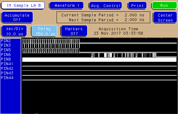
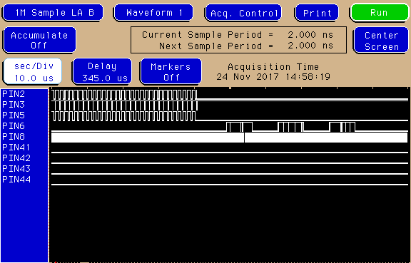
Some words on CPLD startup
11/24/2017 at 19:34 • 1 commentI took some logic analyzer plots of the startup sequence of the unknown FPGA-CPLD communication pins. I don't know what any of it means yet, but maybe it will be of use to someone.
![]()
This plot is taken in timing analysis at 1us/sample, just to show what the whole first two seconds of startup looks like. There is movement up to about 600ms, then basically nothing as the module goes into 'no incoming signal, just sit here and blink' mode
I have zoomed in on most of the transitions, and there's not really a lot going on at most of them, with the notable exception of the two little spikes around the second division. There's actually quite a lot going on around there. The next two plots were taken in timing analysis at 2ns/sample to adequately capture the clock rate.
![]()
Here's the tail end of the first data blip. Pins 2, 3 and 5 have relatively constant transitions with occasional rapid bursts. Pin 6 displays serial data, as theorized in another thread this is likely SOUT data from one of the LED strings. Pin 8 has a fairly regular clock, but this is interesting - during this startup time, the clock measures around 27MHz, but it jumps to 40MHz when the module goes idle. What the point of this would be, I don't know.
![]()
The second blip looks similar but the data on Pin 6 is different, the FPGA must be asking the drivers a different question.
I have posted a Sigrok/PulseView-compatible dump of the first data burst to the Files section. It is missing the data for PIN41 which was lost when my analyzer crashed before the dump finished, but PIN41 doesn't do anything during this time anyway. Hopefully someone can make some sense of this.
-
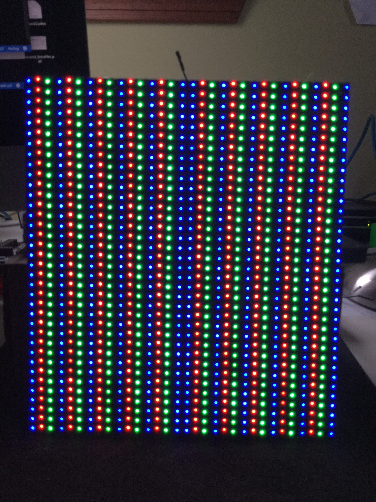
Simple NX4 Test Program
11/24/2017 at 18:30 • 13 commentsI have a simple NX4 test program which displays a BRG pattern on the tile. I will update the program as we discover more secrets. Dot Correction implementation is next on the list.
https://github.com/derekmulcahy/simple_nx4
![]()
-
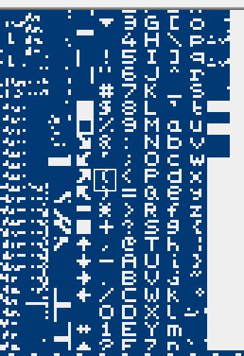
Initial thoughts
11/23/2017 at 04:30 • 1 commentWell I got on the bandwagon and bought 70 of these modules. I hope they all or mostly all work. Anyways, I have been poking through the ROM images posted, and I found a font inside of the parallel flash. It lives around 83180h or so (I will check for more than 1 copy of it... the install PDF claims there's backup firmware in the flash in one of the troubleshooting sections). The font looks like this:
![]()
I used yy-chr to grab it. Interesting that it's 6 pixels high, I guess this is so they can fit 6 lines of it on one of the modules.
Was poking through the EEPROM_panel file too, and it seems to be calibration data and possibly pixel order data too. There's several distinct sections of data. The EEPROM_control file is kind of weird, there's obviously data in here but it doesn't seem to be calibration data, I am not sure what would be living in here. I guess it could be a local copy of adjusted calibration data maybe?
My current working theory is on bootup, the controller will fetch the panel's calibration and control data out of the EEPROM_panel chip and load it into the SRAM (after some kind of processing and possible calibration with the light sensor/LEDs). I guess over time the panel could recalibrate itself too. The SRAM most likely holds the frame buffer as well, and during scanout it reads the pixel data and calibration data and does the fixup.
Reading literature for other similar LED walls, they do a 3*3 matrix multiply for every single pixel to effect the calibration. I am not sure if this does it, but I wouldn't be surprised if it does. It might be interesting to creatively corrupt the RAM contents as it runs to see if anything happens.
Because there is a font in the ROM, this thing most likely has some kind of diagnostics it can perform.
-
OpenNX4 source + binaries posted!
11/15/2017 at 07:00 • 14 commentsA big chunk of NX4 Xilinx code (with precompiled binaries and python code to talk to the tile over UART) just posted: https://github.com/raplin/OpenNX4
Currently the code supports taking to a host over UART (e.g. loading images onto the NX4) and python code is provided to make it do stuff.
It's currently in an 'advanced user' state, there remains one vital thing to figure out on the NX4; how to get the row scanning working (i.e. how to get the CPLD on the LED driver board to play ball).
Once we get that sorted out we're fairly far towards a working, daisy-chainable video tile, controllable by a variety of hosts (Ardunio, embedded linux, etc) using a variety of protocols and doing a variety of 'intelligent display' tricks.
Goal
We should be able to end up with something you can flash onto a tile in a minute or two with a cheap JTAG adapter, and accepts further firmware updates over the wire
The blocker right now is the CPLD (not) doing row scan...
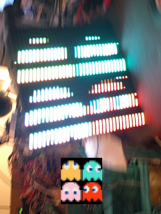
Here's a really, really bad photo where I'm moving the camera so you can see the scanned image (original inset). The tile itself seems high quality; you can get excellent intensity gradients on it, and the 1/6 scan rate w/12-bit CC drivers is a luxury.
![]()
BARCO NX-4 GROUP REVERSING ADVENTURE
This a project for a group of folks working to reverse engineer the Barco NX-4 LED panels.