Ian Hanschen
-
Protocol suggestions
11/06/2017 at 22:18 • 5 commentsHi there,
As someone who's interested in the "reimplement HDL" option for the tiles - I thought a suitable name might be "OpenNX4" (resisting the temptation to run the two n's together) and had a few thoughts/suggesions to throw out there.
For the sake of this discussion, let's say an "end user" is someone who (at least initially) has one or more NX4 tiles and a Raspberry Pi and wants to use them as a video panel (daisychained, with the tiles in a plane or just placed artistically), with minimum extra hassle.
Because the only limit of how many tiles you can daisychain is your power source, your frame rate and your wallet, let's look at how we can get the best frame-rate (=highest speed pixel interface).
The tiles come with an IN and OUT port. The IN port has 2x in and 1x out LVDS pairs, and the OUT port has 2x OUT and 1x IN pairs. The pairs can be used as single-ended i/os as well of course.
As NX4 is FPGA driven it means almost any protocol can be implemented (although HDMI video is not reasonable). You really just want a lot of downstream performance; an upstream link back from the tiles can be arbitrarily slow.
If we look at what protocols are available on typical hacker boards (OPi, RPi, Allwinner, or even Teensies):
I2C up to about 1-2mbps, UART ~4mbps.. and..
SPI (and/or I2S) ports at up to ~100Mbit/s
(There is also SD - as 'make the tile a fake SD card' which is fiddly and takes too many wires in fast 4-bit SD mode)
Another option is that some SBC's have a connector for an LCD display which is usually LVDS, and we could probably provide an interface to that too assuming there are enough pins (or we ignore some of them).
The current crop of cheap allwinner H3 boards are great, and some tricks are possible including running both I2S ports synchronously (=2 bits @ 80+Mhz); they're my fave platform right now, but much of this is doable on a Raspberry Pi too (possibly lower performance).
Suggested configuration
For the sake of discussion let's say you stick an Orange Pi right physically on the back of an NX4 tile, and that's your video processor; you can send it stuff over wifi or ethernet, generate trippy images, play video off SD, whatever. It runs some code that preprocesses and maps the pixels to the tiles, and blasts the result to the first (and subsequent daisychained) NX4 tiles. (You can probably power the Orange Pi off the 4v6 supply in the tile).
First tile in array receives single-ended
So the NX4 is an SPI slave. All our tiles boot up in "spi slave" mode until they hear otherwise.
So from your OPi you run SPI MOSI and SCK over nice short terminated wires into the tile data input. Add MISO so you've got a data stream back (we could connect CS but could also design the protocol so it's not required). This will probably achieve in the ballpark of 30-80Mbps actual throughput.
Even higher performance option : I2S on Allwinner boards; instead of using SPI it's likely possible to use synchronous dual channel I2S; i.e. run PCM0_DOUT and PCM1_DOUT, PCM0_CLK (and PCM0_DIN for a return data channel) which might achieve ~100Mbps.
Daisychained are differential
Ok so that's the first tile, what about daisychaining? Note that we can use the first tile as a "single ended to differential converter" and have the OUT port sending LVDS signals downstream to all the other tiles; hence we gain the noise immunity, longer wire length and general better performance of LVDS for all the other tile data links, however many there are (limited only by your desired frame rate).
Advanced hacker bonus points would be so only one tile needs to be reflashed with different Xilinx code, and it accepts a single-ended input from the linux board and converts it to Barco format output for the other daisychained tiles...
Bottom Line - performance
Ok so if in practice we get say 30mbps data rate with a negligible amount of overhead that isn't actual pixels, what frame rates can we get?
Each tile is 32x36 = 1152 pixels.
Starting simplistically; If we use RGB888 pixel format (with internal 8->12 bit per pixel upscaling in the tile), that's 27.6kbits per tile; at 60fps each tile consumes 1.6Mbit/sec.
If we have 30Mbps usable data rate, we can run 18 tiles (2x9 sets) at 60fps. This seems conservative.
...this is without any fancy tricks of course; we can use <24 bits per pixel quite reasonably with the right encoding, use compressed pixel streams, partial updates, all sorts of things; I'd guess you can double the above performance with some optimization. There also seems to be plenty of processing power in each tile remaining to use doing pixel decompression.
(I would also expect to be able to get >30mbps out of the SPI link if the wiring is reasonably carefully done; currently in my HDL I'm not using a PLL so my SPI receiver is clocked at CLK_40, which limits it to somewhere <20Mhz, but that's easily fixed)
Simple "Barco-lite" setup suggestion
So; a chunky 24v power supply (or several) off ebay, some cables+connectors (possibly the most expensive part) and an Orange Pi, one for each 18 (or more) NX4 tiles.
This setup could display live HDMI video input using one of those ~$30 "HDMI capture" dongles which send H264 frames over ethernet (UDP); these have some latency (maybe 1-2 secs) but may be fine for your use.
The Orange Pi can also of course act as a remote desktop/VNC etc output, video player, etc, but could make a decent replacement for (at least) two Barco NX4 controllers and the main Barco video processor thingy. Obviously put a web interface on it for panel control from your phone... :-)
Large arrays
For a larger array (say 24 tiles wide by 18 high for 768x648 on 432 tiles), you might use one OPi per 36 daisychained tiles (@ 30-60fps) so that's 12 OPi's, which could all be on a 100mbps lan and receive the same multicast H264 stream; extracting their own tile areas from the image.
Alternatively if you don't want to feed your display H264 (i.e. send it raw pixels instead, e.g. from a MAME framebuffer) it's very doable, maybe you'd use ethernet switches with 100M ports and a Gig-E uplink (i.e. practically any ethernet switch on ebay) fanning out to each OPi and then unicast the raw pixels as UDP jumbo frames. -
Some words on the I/O connectors
11/04/2017 at 04:47 • 4 commentsI see Ian posted a preliminary pinout for the input and output connectors. I have some additional information on that topic that I haven't posted yet, so now seems as good a time as any to get that out there.
In a full NX-4 installation, three of these modules are cascaded via the 8- and 9-pin connectors on the rear. That means that all signals necessary for operation of the next panel must be transmitted by the previous one.
Here's a key piece of information that may have been glossed over. FPGA pins 128 and 129 (IP_L06P_0/GCLK8 and IP_L06N_0/GCLK9) are dedicated input pins. These happen to be mapped to output connector pins 5 and 8. Therefore, we can say that the output connector contains two power pins, four output pins, and two input pins. Because the panels are daisy-chained, we can also therefore say that the input connector contains two power pins, four input pins and two output pins.
If you look closely at the layout of the board, there are resistors attached to pins 7 and 8 of the input connector. If you poke around, there are also two similar resistors tied to pins 2 and 3 of the input connector and pins 5 and 8 of the output connector. These appear to be pullup/pulldown or termination resistors for the input lines. Therefore, I assert that the pin directions of the two connectors are:
Input Connector Output Connector 1 - +VIN 1 - +VIN 2 - Input Pair 1N 2 - GND 3 - Input Pair 2N 3 - Output Pair 2P 4 - Output Pair N 4 - Output Pair 1N 5 - Output Pair P 5 - Input Pair P 6 - GND 6 - Output Pair 2N 7 - Input Pair 1P 7 - Output Pair 1P 8 - Input Pair 2P 8 - Input Pair N 9 - ? No discernible destination It would not be unreasonable to assume something like that the dual pairs are a high-speed differential channel for carrying pixel data and consisting of clock and data pairs, and the single pairs are a status bus traveling in the opposite direction for panel configuration and error messages (fan fail, overtemp, etc). There is also a resistor between pins 5 and 8 on the output connector, and pins 3 and 8 on the input connector; based on the rest of my theory and symmetry of design, I'd guess that pins 3 and 8 were the Data bus for pixel data, and pins 2 and 7 would be the Clock. Or I may be missing something and my theory is completely worthless - this is all unconfirmed, which is why I hadn't posted it yet :)
One additional additional note on +VIN. Although things start to respond at only 6V, the input has to be higher than that for everything to work properly. The LT1933 switching regulator that runs the fan puts out 12V, and it needs maybe 2.5V of headroom to do the step-down. So the nominal input VIN has to be at least about 14.5V. That's a weird value, so I'd expect the real input to be somewhere in the 16-24V range.
-
Trimming down members
11/03/2017 at 13:30 • 0 commentsDropping some of the members who haven't contributed - I'm sorry about that. I was eager to have folks join in so I was auto-approving, but please post in the comments if you have something to contribute (or are working on something - that's good enough), and we'll approve your join request. Otherwise, if you've purchased the panels and are waiting for the results, just follow. I want to make sure the folks doing the hard work get the credit.
-
I2C Devices and EEPROM Contents
11/03/2017 at 03:10 • 9 commentsI've mapped all five I2C devices in the assembly to addresses now. They are as follows:
0b0111001x (0x39): LED Panel ambient light sensor
0b1001000x (0x48): LED Panel temperature sensor
0b1001001x (0x49): Control Board temperature sensor
0b1010000x (0x50): LED Panel EEPROM
0b1010001x (0x51): Control Board EEPROMThe ambient light sensor's address corresponds to one option for a Taos part; it responds to a request for register 0x0A with 0x0A, which either means it's a Taos TSL2560 Rev. 10, or it's something completely different that just parrots back the data sent to it (I haven't dug any further into it yet).
I have also dumped the two EEPROMs, and have posted them to the Files section. They are structured differently, but both start with a preamble containing the part number, serial number and manufacture date.
Now go forth and speculate wildly :)
-
Xilinx starter project on github
11/01/2017 at 04:07 • 0 commentsI've pushed a Xilinx ISE starter project configured for the NX-4 board with all of the known pins mapped and outputs defaulted to ground. It's on the GitHub repo.
-
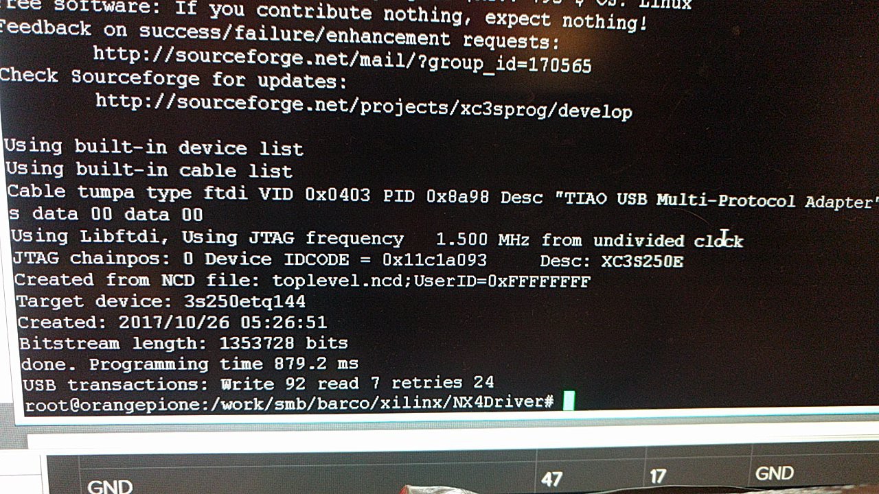
Quick test bitstream for ya
10/31/2017 at 22:13 • 12 commentsI've got a bit carried away in the weeds with adding bells and whistles to my xilinx stuff (and it's broken right now) but I uploaded a .bit and .svf (use whichever your jtag supports), which zips some pixels along the top row of each scan. It's just a very rough thing from last week so you can see some pixels light up.
Programming this image won't affect your board; reset it and it's back to normal.
Note that on this image I used pin 7 on the input connector (that's the male connector on the left of the back, the top-left pin) as a chip reset, so jumper it to GND to make stuff work.
-
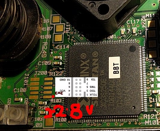
JTAG
10/30/2017 at 04:38 • 2 commentsFYI JTAG connections you may wish to use 2.8v as marked for your JTAG interface bus voltage instead of the 3v3 provided on the jtag connector. I honestly think 3v3's fine but... someone would have to disprove my experience by doing it and not having the $20 Xilinx blow up.
![]()
It looks like pretty much any JTAG interface is fine; there are a bunch of tools; OpenOCD has some JTAG support but I didn't see Spartan 3E programming in there (it looks a bit light on fpga support unless I was looking at the wrong thing).
You can use the Xilinx ISE tools and the "device programmer" part can generate a kinda "jtag recording" (SVF file I think?) which is so simple almost any JTAG programmer can replay it to program a device.I tend to use a lot of embedded linux (currently Orange Pi boards which are my default hardware platform now) so "xc3sprog" works fine with an FT2232-based JTAG interface.
If anyone wants a buying suggestion for a JTAG interface; If you want a quality tool the "TIAO tumba" FT2232 board (relatively pricey at $30) has all the level shifting and jumper doodads you want and looks to be a perpetually handy thing to have around the house. -
Control Board FPGA Pinout
10/27/2017 at 07:48 • 0 commentsI might be missing a few connections yet which I'll correct as I come across them, but here is the pinout of the XC3S250E FPGA on the control board. Note that the SRAM and the Flash share an interface bus. Also note that the JTAG interface is 2.5V logic.
Pin Function Pin Function 1 PROG_B (Pullup to +2.5V) 73 GND 2 LED_L1_SIN 74 SRAM_A16; FLASH_A15 3 LED_L2_SIN 75 SRAM_A15; FLASH_A14 4 LED_L3_SIN 76 SRAM_A14; FLASH_A13 5 LED_R1_SIN 77 SRAM_A13; FLASH_A12 6 78 7 LED_R2_SIN 79 VCCO_1 (+3.3V) 8 LED_R3_SIN 80 VCCINT (+1.2V) 9 VCCINT (+1.2V) 81 SRAM_A12; FLASH_A11 10 LED_XERR 82 SRAM_A11; FLASH_A10 11 GND 83 FLASH_RESET# 12 84 13 VCCO_3 (+3.3V) 85 SRAM_A10; FLASH_A9 14 LED_L4_SIN 86 SRAM_A9; FLASH_A8 15 LED_L5_SIN 87 SRAM_A8; FLASH_A7 16 LED_L6_SIN 88 SRAM_A7; FLASH_A6 17 LED_R4_SIN 89 18 90 GND 19 GND 91 SRAM_A6; FLASH_A5 20 LED_R5_SIN 92 SRAM_A5; FLASH_A4 21 LED_R6_SIN 93 SRAM_A4; FLASH_A3 22 LED_CAL_SIN 94 SRAM_A3; FLASH_A2 23 CPLD_PIN_44 95 24 CPLD_PIN_6 96 SRAM_A2; FLASH_A1 25 I2C_SCL 97 SRAM_A1; FLASH_A0 26 I2C_SDA 98 SRAM_A0; FLASH_DQ15/A-1 27 GND 99 GND 28 VCCO_3 (+3.3V) 100 VCCO_1 (+3.3V) 29 101 30 VCCAUX (+2.5V) 102 VCCAUX (+2.5V) 31 SRAM_CE# 103 SRAM_WE#; FLASH_WE# 32 LED_XLAT 104 FLASH_CE# 33 LED_MODE 105 FLASH_OE# 34 LED_BLANK 106 35 SRAM_OE# 107 FLASH_RY/BY# 36 108 JTAG_TMS 37 GND 109 JTAG_TDO 38 110 JTAG_TCK 39 LT1933_ENABLE 111 FAN_TACHOMETER 40 112 INPUT_CONN_PIN_5 41 113 INPUT_CONN_PIN_4 42 VCCO_2 (+3.3V) 114 43 SRAM_BHE# 115 VCCINT (+1.2V) 44 SRAM_BLE# 116 INPUT_CONN_PIN_7 45 VCCINT (+1.2V) 117 INPUT_CONN_PIN_2 46 GND 118 GND 47 119 INPUT_CONN_PIN_8 48 120 INPUT_CONN_PIN_3 49 VCCO_2 (+3.3V) 121 VCCO_0 (+2.5V) 50 SRAM_IO7; SRAM_IO15; FLASH_DQ7 122 51 SRAM_IO6; SRAM_IO14; FLASH_DQ6 123 CPLD_PIN_8 52 SRAM_IO5; SRAM_IO13; FLASH_DQ5 124 CPLD_PIN_3 53 SRAM_IO4; SRAM_IO12; FLASH_DQ4 125 CPLD_PIN_2 54 SRAM_IO3; SRAM_IO11; FLASH_DQ3 126 CPLD_PIN_5 55 GND 127 GND 56 OSC_40MHz 128 OUTPUT_CONN_PIN_5 57 129 OUTPUT_CONN_PIN_8 58 SRAM_IO2; SRAM_IO10; FLASH_DQ2 130 OUTPUT_CONN_PIN_7 59 SRAM_IO1; SRAM_IO9; FLASH_DQ1 131 OUTPUT_CONN_PIN_4 60 DIAGNOSTIC_LED_YELLOW 132 CPLD_PIN_43 61 GND 133 GND 62 DIAGNOSTIC_LED_RED 134 OUTPUT_CONN_PIN_3 63 SRAM_IO0; SRAM_IO8; FLASH_DQ0 135 OUTPUT_CONN_PIN_6 64 VCCO_2 (+3.3V) 136 65 VCCAUX (+2.5V) 137 VCCAUX (+2.5V) 66 FLASH_A19 138 VCCO_0 (+2.5V) 67 FLASH_A18 139 LED_SCLK 68 FLASH_A17 140 LED_GSCLK 69 141 70 SRAM_A17; FLASH_A16 142 CPLD_PIN_42 71 DIAGNOSTIC_LED_ORANGE 143 CPLD_PIN_41 72 DONE (Pullup to +2.5V) 144 JTAG_TDI -
Lights on
10/26/2017 at 21:24 • 0 commentsSimple/ugly proof of concept from last night; no row-muxing yet but the lights come on..
-
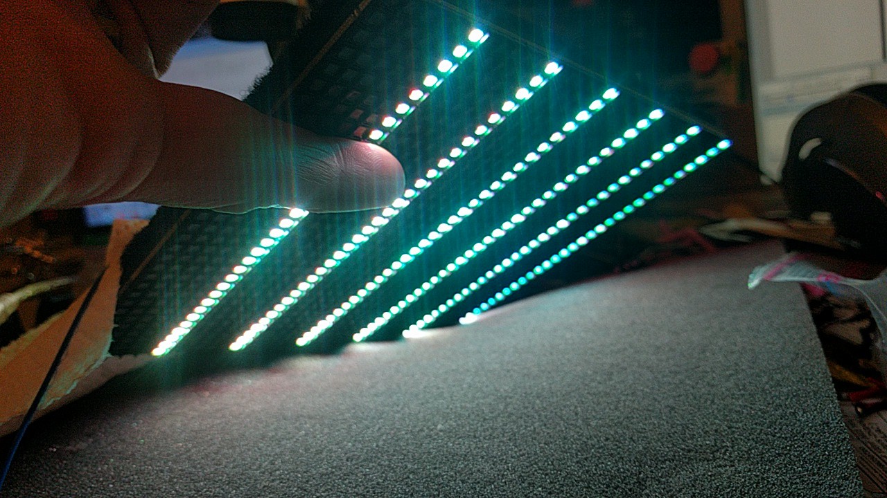
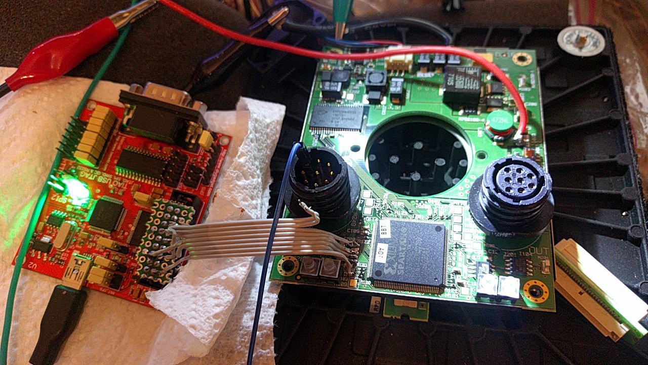
Progress from Richard Aplin
10/26/2017 at 13:52 • 0 commentsFew quick photos; got the LEDs lighting up with a homemade FPGA bitstream. Not figured out the row scan quite yet..
![]()
![]()
![]()
BARCO NX-4 GROUP REVERSING ADVENTURE
This a project for a group of folks working to reverse engineer the Barco NX-4 LED panels.