Ian Hanschen
-
LED Arrangement
10/26/2017 at 02:29 • 0 commentsI tried to describe this in words, but I think something was lost in translation. Much easier with a photo.
![]()
The panel is divided into twelve segments of 16x6. Each segment is driven by three Texas Instruments TLC5941 16-channel LED drivers. Each driver controls one color of the tri-color LEDs. The three drivers have their serial data cascaded, with the first controller in the cascade being Red, then Green, then Blue.
The 96 LEDs in the segment are controlled by only 16 driver channels by multiplexing the rows' LED anode voltage (TLC5941 switches the cathode side). Each of the 36 rows has a transistor between the panel's +4.5V input and the LED anodes. All like-numbered rows' transistors are connected to a common control pin on the CPLD. The CPLD cycles through them in sequence as instructed by the FPGA, synchronized with the incoming display data.
Take care when rewriting HDL for the FPGA. Because the LEDs are expecting to be run at only 1/6 duty cycle, they may theoretically be damaged if they are not cycled as quickly by user HDL. (For experimenting, consider using the calibration LEDs on the rear of the panel, which are not multiplexed.)
-
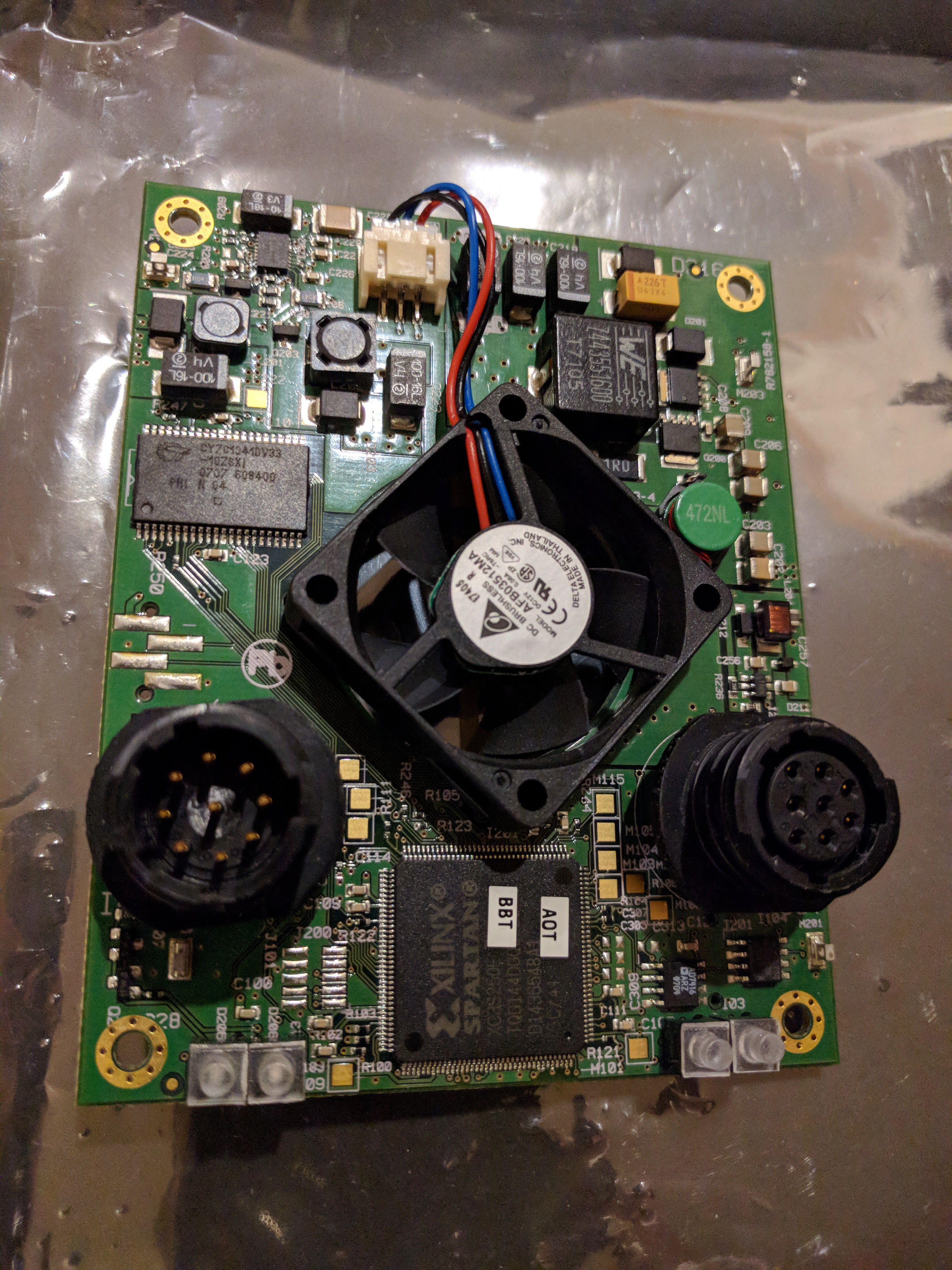
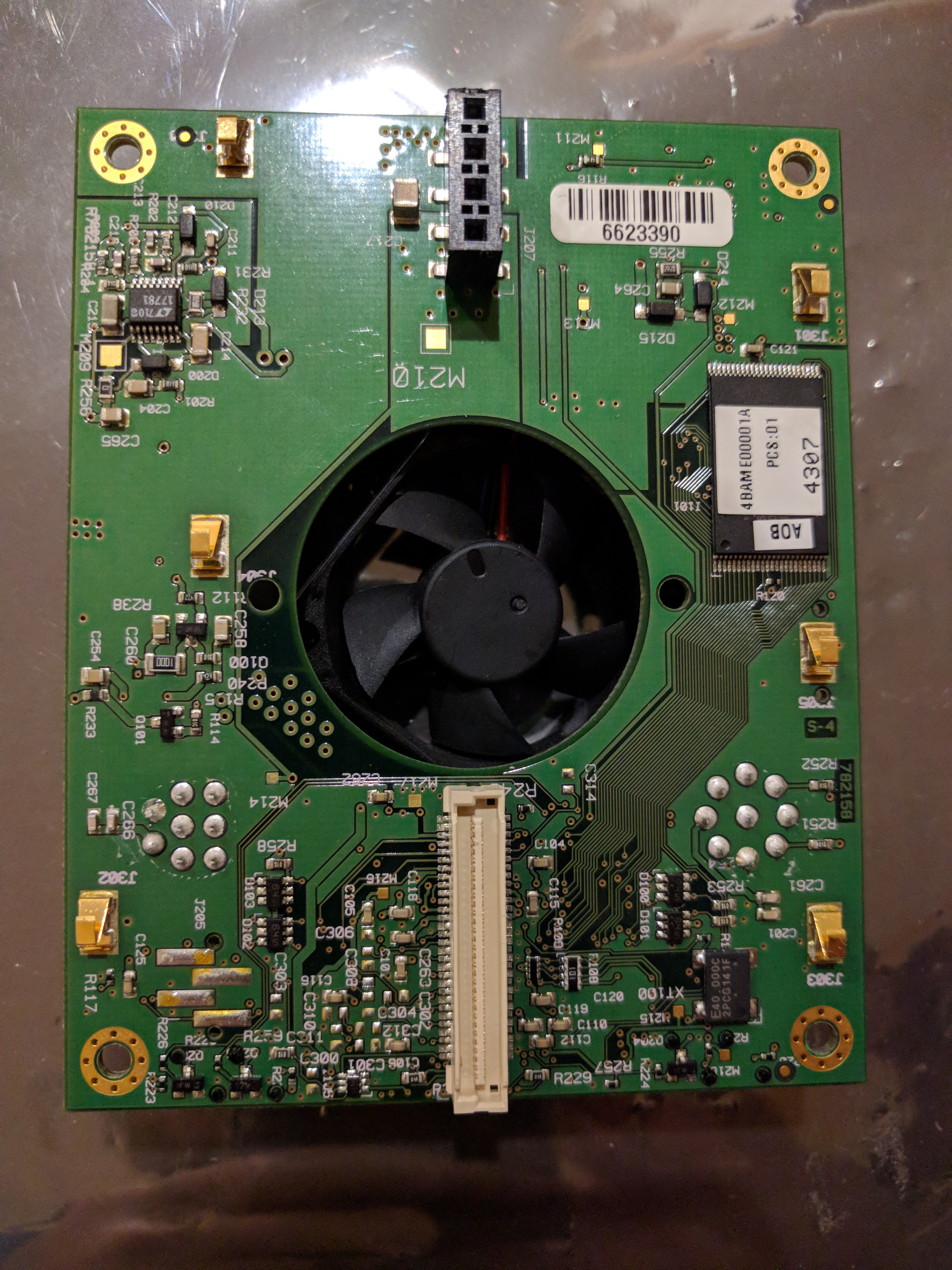
Board Photos
10/26/2017 at 01:33 • 0 commentsHere are some poorly-lit photos I took of the assembly.
Control Board - Front
![]()
Control Board - Rear
![]()
LED Panel - Front
![]()
LED Panel - Rear
![]()
-
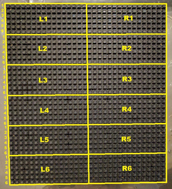
Pinouts for LED panel connectors
10/24/2017 at 04:21 • 0 commentsAs viewed looking at the rear of the LED panel. The panel is arranged as a 36row x 32col grid. LEDs are split into 16 left and 16 right columns, with every six rows driven by three cascaded drivers. From right to left, the first driver drives Red subpixels, the second Green and the third Blue. Anode voltage is switched to each of the six rows of LEDs in sequence via a transistor controlled by the CPLD.
There are three I2C devices on the LED panel, an EEPROM, a temperature sensor and an ambient light sensor used for brightness calibration.
Most of the LED driver control pins are brought out to the data connector by way of two buffers. The remaining signals (SOUT for each driver string) are fed to the CPLD.
Power connector:
4 GND 3 GND 2 +4.56V 1 +4.56V Data Connector:
CPLD_PIN_6* 60 30 VIN CPLD_PIN_44* 59 29 VIN CPLD_PIN_43* 58 28 GND CPLD_PIN_42* 57 27 I2C_SDA CPLD_PIN_41* 56 26 I2C_SCL LED_GSCLK 55 25 LED_BLANK LED_XLAT 54 24 LED_MODE CPLD_PIN_8* 53 23 CPLD_PIN_2* CPLD_PIN_5* 52 22 CPLD_PIN_3* +3.3V 51 21 +3.3V +3.3V 50 20 +3.3V +3.3V 49 19 +3.3V +3.3V 48 18 +3.3V GND 47 17 GND GND 46 16 LED_XERR GND 45 15 LED_CAL_SIN LED_R6_SIN 44 14 GND GND 43 13 LED_R5_SIN LED_R4_SIN 42 12 GND GND 41 11 LED_L6_SIN LED_L5_SIN 40 10 GND GND 39 9 LED_L4_SIN LED_R3_SIN 38 8 GND GND 37 7 LED_R2_SIN LED_R1_SIN 36 6 GND GND 35 5 LED_L3_SIN LED_L2_SIN 34 4 GND GND 33 3 LED_L1_SIN GND 32 2 GND GND 31 1 LED_SCLK *CPLD pins are not yet mapped to functions. CPLD functions include cycling through rows, routing SOUT data from LED drivers, and six pins mapped to transistors scattered across the board with yet unknown function.
BARCO NX-4 GROUP REVERSING ADVENTURE
This a project for a group of folks working to reverse engineer the Barco NX-4 LED panels.