Paul Andrews
-
Retrospective
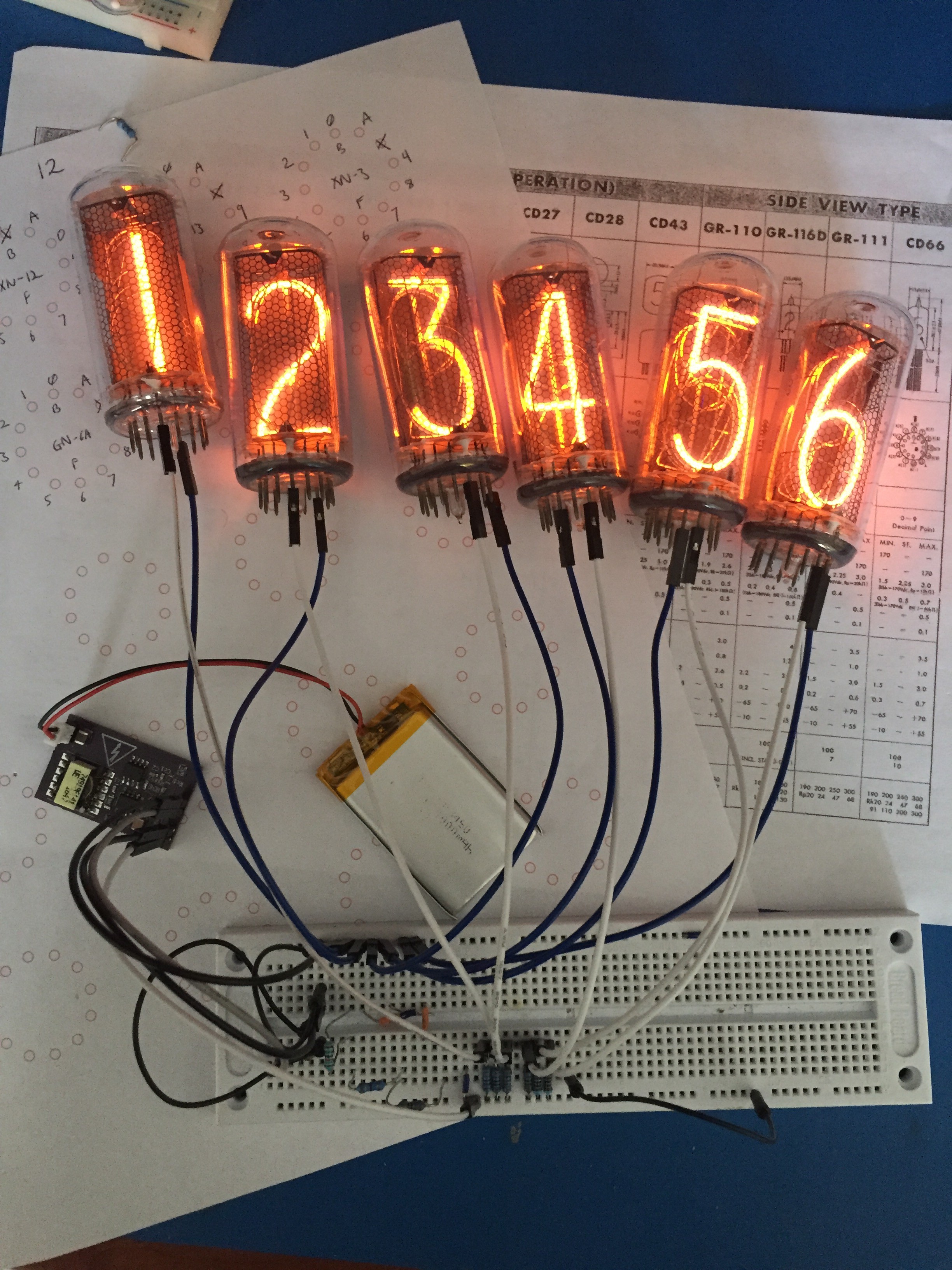
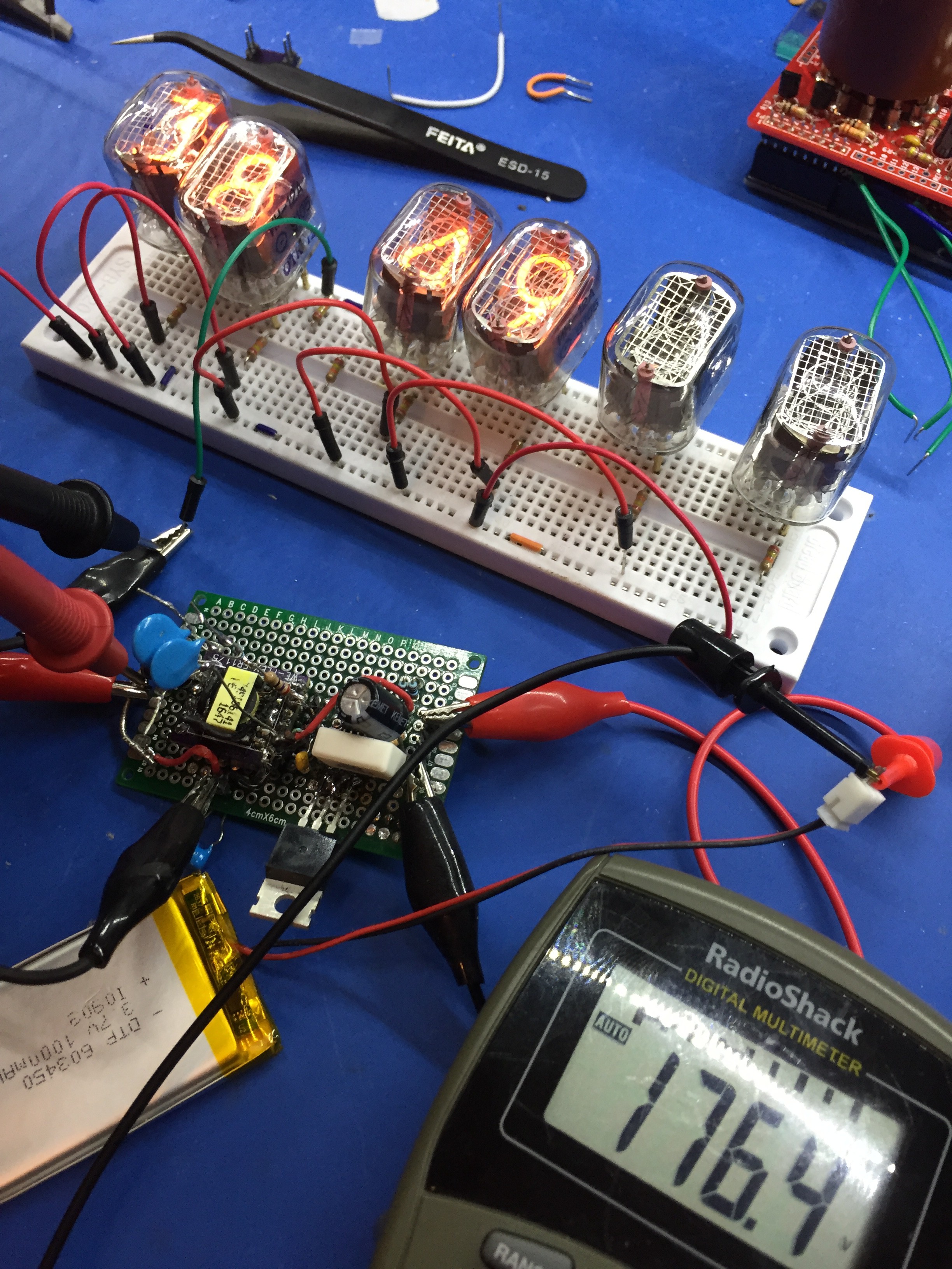
03/25/2018 at 20:59 • 0 commentsA few months on, and I am very pleased with this power supply. I use it in all my Nixie clock projects. The version I use all the time is the one with the WE-FLEX transformer. As it seems to be necessary these days to show that it can drive a bunch of IN-18 tubes from a single LiPo, here is my power supply doing just that:
![]()
I also made a version that produces 240V out, so I could drive IN-28 tubes. To do this I just changed the resistor values in the feedback network. So R2 became 8.66K instead of 10.2K and R3 became 24.9K instead of 33K. That is one of the benefits of knowing your power-supply inside-out: You can easily modify it to suit your own purposes. Or fix it if your transformer goes up in smoke, like that one did when I over-drove it. Now it has a larger current-limiting resistor too.
-
Wrap-up
11/10/2017 at 01:49 • 0 commentsYou can get the board on OSHPark. The full KiCAD project and LTSpice model is in my Github repo. There is a full BOM with digikey part numbers in the files section of this project and in the Github repo.
BTW, I tried reducing Rsense to 0.04Ω. The temperature of the transformer peaked at 160°F at an ambient of 70°. Still well below the absolute maximum of 257°F. I will produce a set of figures for this configuration too, as the supply can provide a lot more current with this lower value of Rsense
![]()
And the MOSFET:
![]()
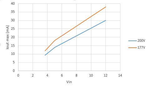
A chart showing the maximum current for a given input and output voltage. I determined this from the readings that follow, by picking the maximum current I could measure before Vout started to be un-regulated. So another way of saying this is that it shows the maximum current for a regulated Vout.
![]()
There might be thermal issues with running at these maximum currents. I couldn't really measure that because my load resistors need some serious heat sinks added first.
In the readings below it is useful to note that for a given load and Vout, the output current remains constant regardless of the input voltage (until the output voltage becomes unregulated)
Readings for a Vout limit of 200V:
12V in Rload Vout Iout (mA) Vin Iin (mA) Eff 19.31 199.8 10.40 11.96 237.90 0.73 14.64 199.7 13.70 11.96 298.20 0.77 10.00 199.4 20.06 11.95 414.00 0.81 6.86 199.1 29.23 11.93 595.00 0.82 4.65 188.4 40.00 11.88 765.00 0.83 5V in Rload Vout Iout (mA) Vin Iin (mA) Eff 19.31 199.3 10.38 4.80 600.00 0.72 14.64 199.2 13.68 4.72 717.00 0.81 10.00 177.2 17.82 4.63 865.00 0.79 3.7V in Rload Vout Iout (mA) Vin Iin (mA) Eff 19.31 199.0 9.30 3.67 865.00 0.58 14.64 181.0 12.30 3.65 890.00 0.69 10.00 146.0 14.00 3.49 906.00 0.65 Readings for a Vout limit of 177V:
12V in Rload Vout Iout (mA) Vin Iin (mA) Eff 19.31 177.8 9.26 11.97 195.50 0.70 14.64 177.7 12.20 11.96 243.10 0.75 10.00 177.6 17.86 11.96 345.50 0.77 6.86 177.3 26.00 11.94 471.00 0.82 4.65 177.0 38.23 11.91 678.00 0.84 5V in Rload Vout Iout (mA) Vin Iin (mA) Eff 19.31 177.2 9.22 4.84 502.00 0.67 14.64 177.2 12.14 4.77 620.00 0.73 10.00 177.0 17.76 4.63 870.00 0.78 6.86 152.0 22.40 4.60 930.00 0.80 3.7V in Rload Vout Iout (mA) Vin Iin (mA) Eff 19.31 177.4 9.24 3.82 610.00 0.70 14.64 177.0 12.17 3.64 900.00 0.66 10.00 144.2 15.00 3.49 914.00 0.68 Here is my new test load rig. An extra resistor and a smaller form factor! I really need to get some heatsinks though. Or even better, an actual test load!
![]()
Here's a much more attractive test load being driven by a liitle LiPo battery:
![]()
-
Final Component Selection
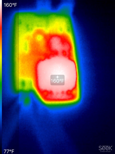
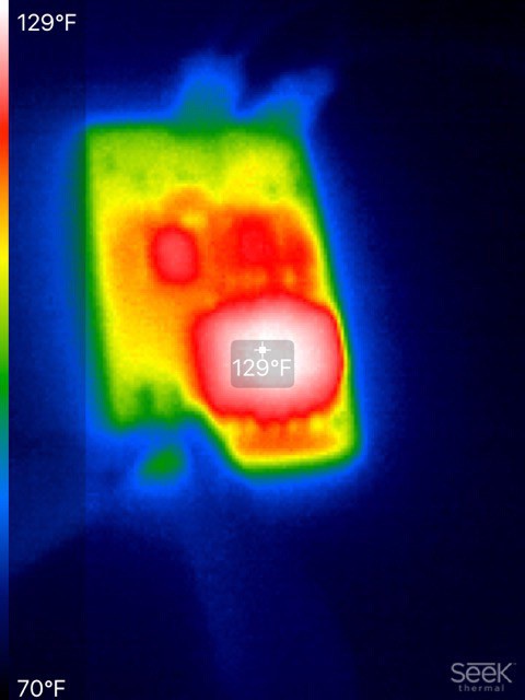
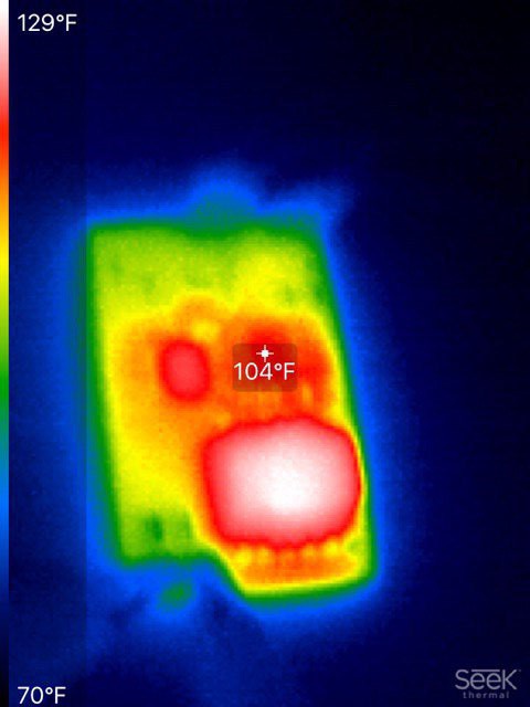
11/08/2017 at 15:12 • 0 commentsI got my thermal camera, so the results are in! It looks like the peak temperature I have managed to get for the transformer is 129°F. Here are some pictures. The first shows the temperature of the transformer. This is when the power supply is producing 20mA at 200V with 12V in:
![]()
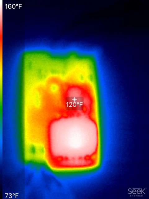
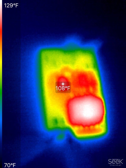
Next up, the controller:
![]()
And next the MOSFET:
![]()
Is that OK? Well the data sheet for the transformer says:
It is recommended that the temperature of the part does not exceed +125°C under worst case conditions.
125°C is 257°F, so we are well under that. These measurements were taken with an ambient temperature of around 70°F. We could expect worse behavior in a closed case, but I think we may still have some headroom, so it could be that the current sense resistor value that I chose could be reduced some. I will try this with a 0.04Ω resistor and check the temperatures again.
I will list the final component values in a moment, but for now here are some performance results:
12V Rload (K) Vout Iout (mA) W Vin Iin (mA) W Eff 20 199.6 10.40 2.08 11.96 238 2.85 0.73 15 199.5 13.70 2.73 11.96 298 3.56 0.77 10 199.2 20.00 3.98 11.94 415 4.96 0.80 20 177.6 9.26 1.64 11.96 195 2.33 0.71 15 177.5 12.18 2.16 11.96 243 2.91 0.74 10 177.4 17.84 3.16 11.96 347 4.15 0.76 5V Rload (K) Vout Iout (mA) W Vin Iin (mA) W Eff 20 192.4 10.00 1.92 4.85 500 2.43 0.79 15 172.6 11.84 2.04 4.84 502 2.43 0.84 10 141.0 14.17 2.00 4.8 508 2.44 0.82 20 177.0 9.22 1.63 4.85 500 2.43 0.67 15 172.5 11.81 2.04 4.84 502 2.43 0.84 10 141.0 14.18 2.00 4.8 508 2.44 0.82 3.7V Rload (K) Vout Iout (mA) W Vin Iin (mA) W Eff 20 174.0 8.80 1.53 3.6 373 1.34 1.14 15 154.0 10.34 1.59 3.6 370 1.33 1.20 10 130.0 12.80 1.66 3.6 364 1.31 1.27 20 172.0 8.80 1.51 3.6 380 1.37 1.11 15 153.0 10.30 1.58 3.6 373 1.34 1.17 10 129.0 12.70 1.64 3.6 370 1.33 1.23 For each input voltage, there are two sets of numbers. The first set is for a Vout limit of 200V. The second set is for a Vout limit of 177V. Here are some takeaways:
- My measurements for 3.7V are clearly wrong somewhere, because they give an efficiency of > 1!
- Ignoring that, we are hitting efficiencies of between 70% and 80%, which is pretty good!
- We can get 20mA out of it if we put 12V in. We could probably get more, but my test equipment (such as it is) can't go lower than a 10K load without starting a fire. In fact, the thermal camera shows that my 10K load resistor was hitting 400°F as it is! Anyone want to buy me some lab equipment? 20mA will power just about any 6 tube clock.
- On battery, we can get 8mA out, which is enough for 4 to 6 small tubes. Which is fine.
- On USB (aka 5V), we can get roughly 12mA out at a decent voltage. That is good for a lot of tube types. If I can decrease Rsense, so I can get more current flowing, we could improve these numbers.
- The voltage regulation starts to fail as load goes up and input voltage drops. Again, I know from experience that if I can drop Rsense, I can get a more stable output voltage
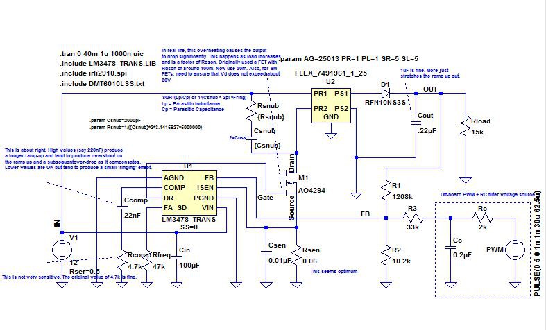
So here is the final circuit diagram:
![]()
- The MOSFET is an AO4294. This has a 100V Vds and a very low Rds(on). Other options I tried tended to get a bit warm.
- Rsen is 0.06Ω.
- Rfreq is 47K.
- Rsnub is 249Ω
- Csnub is 360pF.
- The diode is an ES1FL R3G.
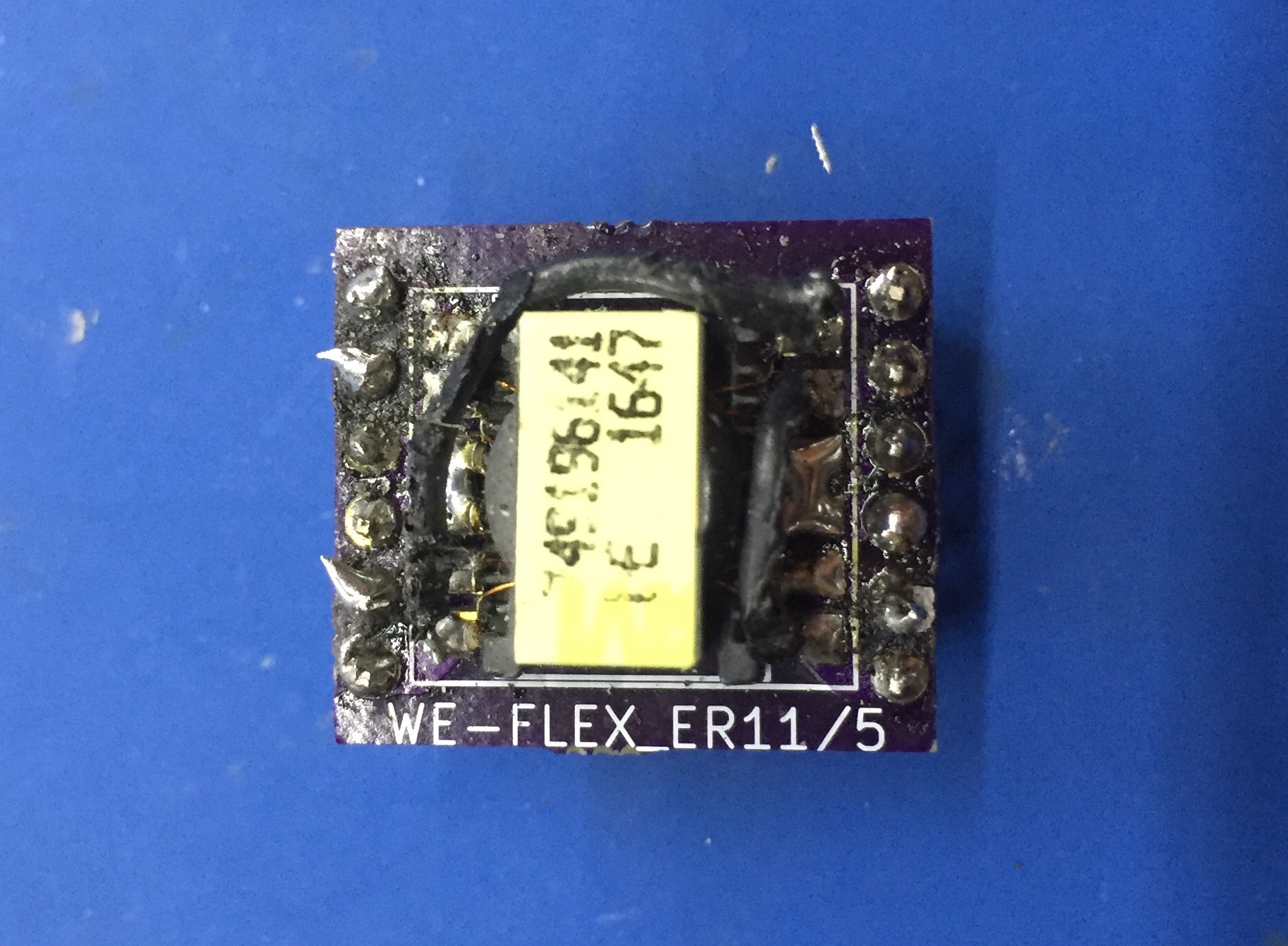
- The transformer is a Wurth ER11/5 - order code 749196141.
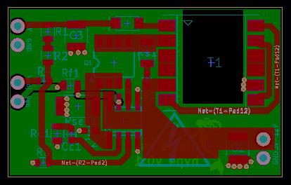
Here is a picture of the board layout:
![]()
-
Adding controls
11/06/2017 at 15:05 • 0 commentsFor the final design, I also wanted to be able to provide a means to enable/disable the power supply and vary the output voltage.
Enable
Enabling/disabling the power supply is necessary if we want to implement tube blanking:
- We can turn the nixie tubes on or off based on a schedule. This is typically done to extend the lifetime of the tubes.
- In a battery powered clock, we only want the tubes on when the user is actively looking at the clock, otherwise we will run out of battery pretty fast.
Note that this is not used for dimming the display - we don't want to turn the entire supply on and off really fast. This is better done using direct control of the current flowing through the tubes themselves.
The LM3478 already has an enable pin, so we can use that in our design.
Voltage
Varying the output voltage is handy for several reasons:
- At low input voltages, the power supply is more able to regulate itself if the output voltage is also lower.
- Other applications of the power supply might require a different output voltage.
There are a couple of solutions to varying the output voltage, but the one that I went for is explained in an article by Simon Bramble. This solution provides several benefits:
- It enforces a limit on how high the voltage can go.
- It allows us to vary the voltage from zero to that limit.
- It allows us to control the voltage using PWM from an MCU.
- It doesn't require a potentiometer on the board itself.
It has some drawbacks too:
- It requires more breadboard wiring to set the output voltage. An on-board potentiometer would provide a simpler solution.
If the design is integrated directly with a clock - rather than being a separate power supply board - you could just set the voltage to whatever you need directly.
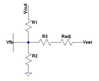
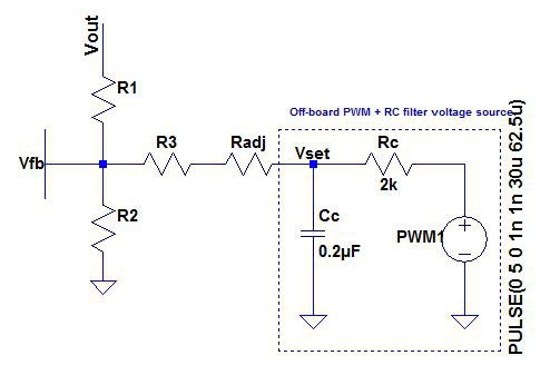
Anyway, this is the basic resistor setup that I will be using. R1 and R2 are already part of the design. The new part is R3 to some voltage Vset. We also add Radj in series - R3 will be fixed:
![]()
So, directly from Simon Bramble: The current flowing through R1 plus the current flowing through R3+Radj must equal the current flowing through R2, because no current flows into Vfb. So we have (folding Radj into R3 for now):
In our case Vfb is 1.26. If we substitute that in and re-arrange for Vout, we get:
The first term is just the regular equation, without R3 and Vset. The second term shows the effect of including R3 and Vset. For now, let's assume that Vset and Radj are zero. It is clear that as R3 increases, the effect of the second term is lessened. At the limit, if R3 is infinite, the second term has no effect at all. As R3 decreases in size, the second term adds to the value of Vout. If R3 is is zero, we are in trouble, so we must choose some minimum value for R3.
If we allow Vset to increase, we can see that the second term reduces the value of Vout. The lowest value for Vout is zero. I will arbirtrarily choose 5V to be the highest value of Vset, because it is a common logic level. So we want Vout to be 0V when Vset = 5V.
Further, to make things simple, I will arbitrarily choose R2 to be 10K. This is what Simon did, and it as about right if we want R1 to be large (which we do). So, now we have two equations:
And
Equating the two, we get:
Or:
Plugging back into the first equation, we get:
- R3 = 30K
- R1 = 1,200K
Because of the voltage rating of regular resistors, we will use two resistors in series for R1 of around 600K. The nearest standard one is 604K, so R1 will be 1208K. Because this is slightly higher, we will use a 10.2K resistor for R2 to compensate. So we have:
- R1 = 1,208K
- R2 = 10.2K
- R3 = 30K
If we plug these numbers back in to our equations (using a spreadsheet, it is way easier), we get:
- Vset = 0V, Vout = 201V
- Vset = 5V, Vout = 0V
- Vset = 2.5V, Vout = 100.5V
- Vset floating, Vout = 150V
We can adjust Vout anywhere in between by adding Radj. e.g. with Radj = 20k
- Radj = 20k, Vset = 0V, Vout = 181V
- Radj = 20k, Vset = 5V, Vout = 60V
- Radj = 20k, Vset = 2.5V, Vout = 120V
Etc.
It was slightly before this, that I realized that this is exactly what John Taylor did with his power supply, even down to the resistor values. I honestly didn't reverse-engineer his power supply! It was basically driven from Simon's design and the fact that Vfb is almost the same on the chip I use and the chip that John uses.
So now, the circuit looks like this:
![]()
You may notice that the MOSFET is yet another model: An IRL3103, and that there is a different transformer symbol. That is because I was modelling the circuit for a different transformer.
PWM Voltage Control
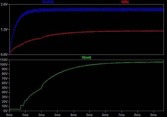
To control the voltage using a PWM signal we need to build an RC filter to smooth out the oscillations. In the image below we have set up a 5V source with a PWM frequency of 16KHz and a 50% duty cycle. We have added an RC filter with a a cutoff frequency of about 1/4 that:
![]()
Cutoff frequency of the RC filter is given by this equation:
Rc should be << R3 + Radj.
Here are the results of a simulation for that:
![]()
Note that Vset (Vn005 in the graph) comes out at around 2.3V, so Vout is correspondingly higher at around 105V.
-
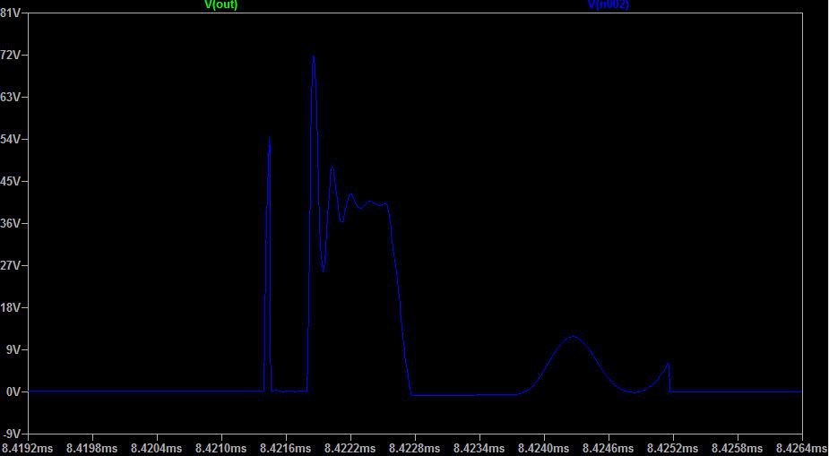
Ringing
11/04/2017 at 23:50 • 0 commentsIt is time to address the ringing problem that we have seen in the simulation, and in the prototype. This analysis uses the AON6242 used in the original simulation.
The problem is that when the MOSFET turns off an oscillation in the drain voltage is initiated caused by the leakage inductance of the primary transformer winding and the output capacitance - Coss - of the MOSFET. The issue with this is that it can cause the peak voltage on the drain of the MOSFET to exceed the the rating - the ringing voltage can often be twice the reflected voltage, which is kind of unnecessary.
Here is a picture from the simulation showing the un-damped oscillations:
![]()
Here is what it looks like with some damping:
![]()
What you can see here is that the reflected voltage is around 40V. This is what the MOSFET should have to deal with. The peak voltage in this is down to 80V from 120V, which is an improvement, and the oscillations die out very quickly.
There are a couple of solutions. One is to clamp the voltage with a diode. Another is to dampen the oscillations with an RC (Resistor-Capacitor) snubber. Another solution is to do both. I chose to damp the oscillations with a snubber, because we also don't want the circuit to be radiating EMI, so dampening the oscillations is a good thing to do anyway. I chose the topology in this application note. I started by setting the capacitance (Csnub) to 2xCoss. This halves the frequency of the ringing. The resistor value is set to:
With LTSpice we can measure the ringing frequency as follows:
![]()
So the frequency is 9MHz. From the datasheet for the AON6242, Coss is 540pF, so Csnub is around 1200pF. This gives an Rsnub of 15Ω.
You can see that the frequency has approximately halved in this image:
![]()
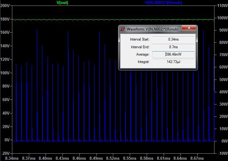
We can damp the ringing more by increasing the resistor value, but this will dissipate more power. According to LTSpice, the RC snubber dissipates this much power:
![]()
About 0.4W. This is quite a lot, so I am left wondering if there is a better way to do this, or even if it is necessary at all.
The whole circuit now looks like this:
![]()
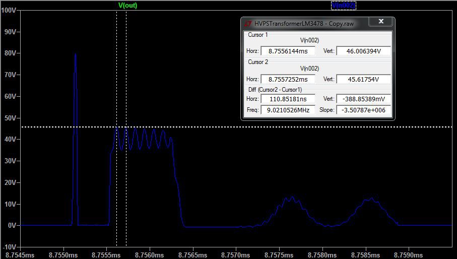
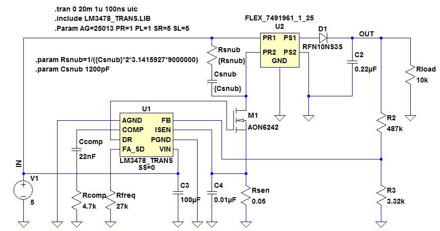
Here is what I measure with the actual prototype with no snubber (remember this uses an IRL640A, not an AON6242):
![]()
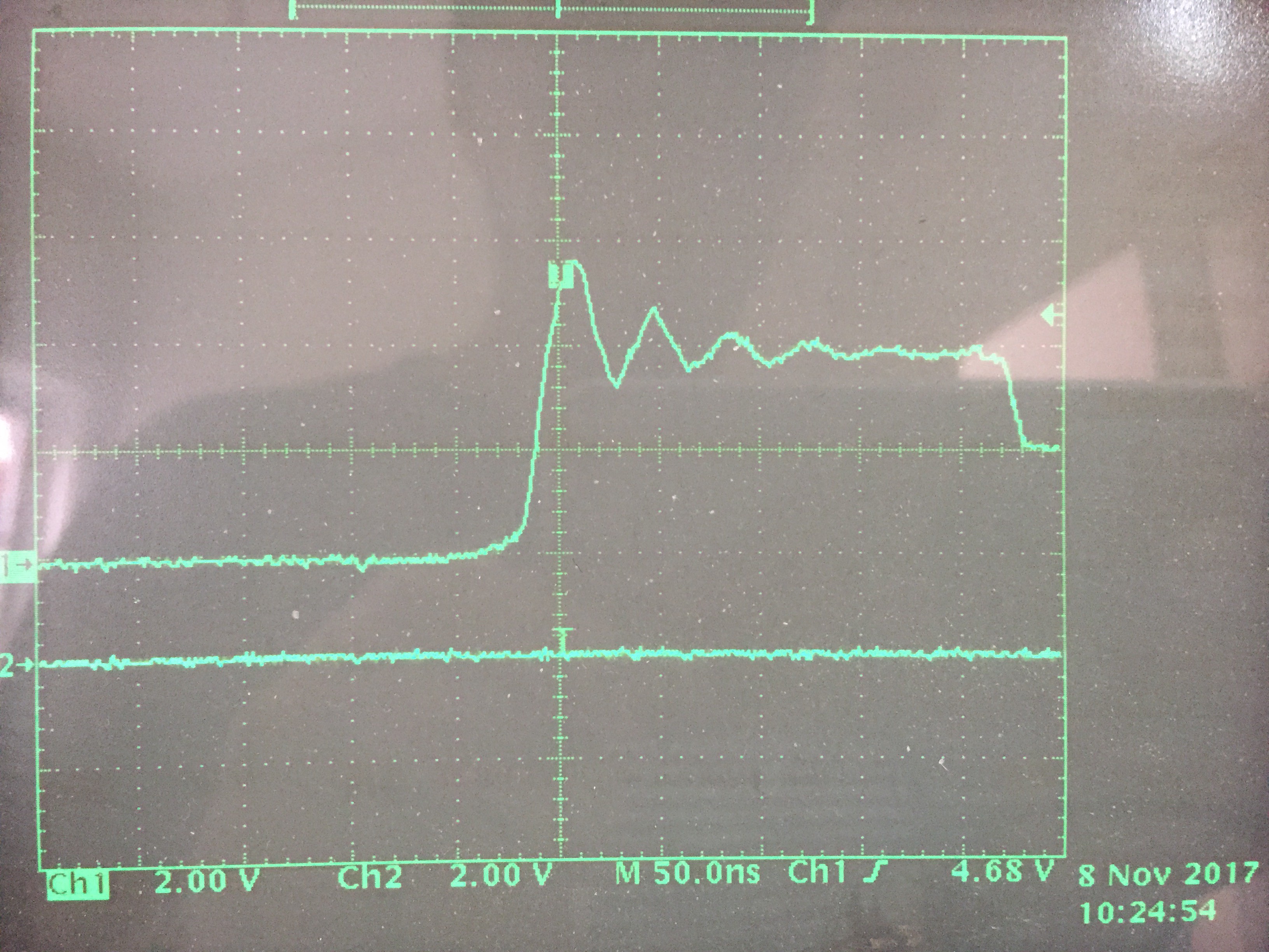
Note that channel one has a 10x probe, so each square is actually 20V. We can see that the peak is only around 60V, so there is no real need for a snubber here, but we will continue just to test it out. Note that the frequency of the ringing is 1/50ns or 20MHz. Coss for the IRL640A is only 200pF, so we only need a Csnub of 400pF, and our Rsnub is now 20Ω. Here is what it looks like after applying the snubber:
![]()
So yeah. It's damped. Seems a bit unnecessary with this prototype, but I will leave it in the circuit when I have some actual PCBs fabbed - I can always leave it unpopulated, but I can't add it after the fact.
BTW, I re-ran the simluation with the IRL640A, and the frequency of the ringing is very similar: 17MHz.
-
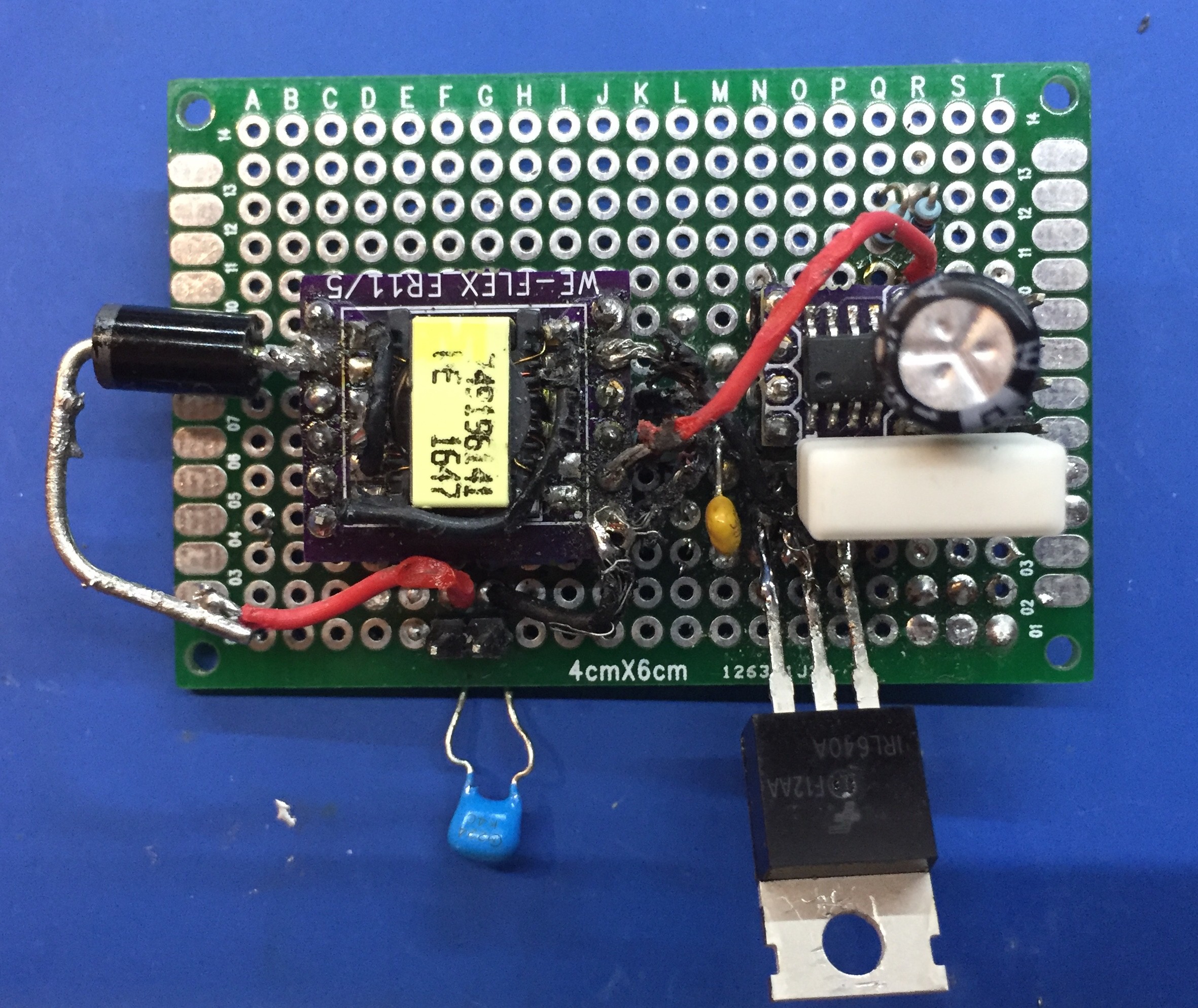
Prototype
11/03/2017 at 02:19 • 2 commentsAfter I had spent a month or so messing with LTSpice, I decided that I really needed to build something to try it out. From what I had read, trying to prototype this power supply using a breadboard would not be a good idea. Breadboards have too much additional resistance, capacitance and inductance that would just mess up the results. The next best thing, I decided, was to use perfboard - with this I would hopefully suffer less from all the drawbacks of breadboard.
I started by designing an adapter for the transformer and having it fabbed at OSHPark. I also ordered a SOIC8 adapter from there for the LM3478. This makes it easier (i.e. possible) to incorporate them into perfboard. Then I ordered all of the parts I thought I would need from Digikey. For the key components such as the output capacitor, the current sense resistor and the loop compensation resistor and capacitor, I ordered the values from the simulation (or close to them) and a few either side. It turns out that this was really important - the performance of the physical circuit was very much affected by some of these values.
This was the wiring diagram for the transformer:
![]()
This is what it looked like all wired up:
![]()
It looks a real mess in that picture, because that is what it looks like now, after it had been inserted, removed and re-wired several times. It still works though!
This is what the finished prototype looked like (or looks like now!):
![]()
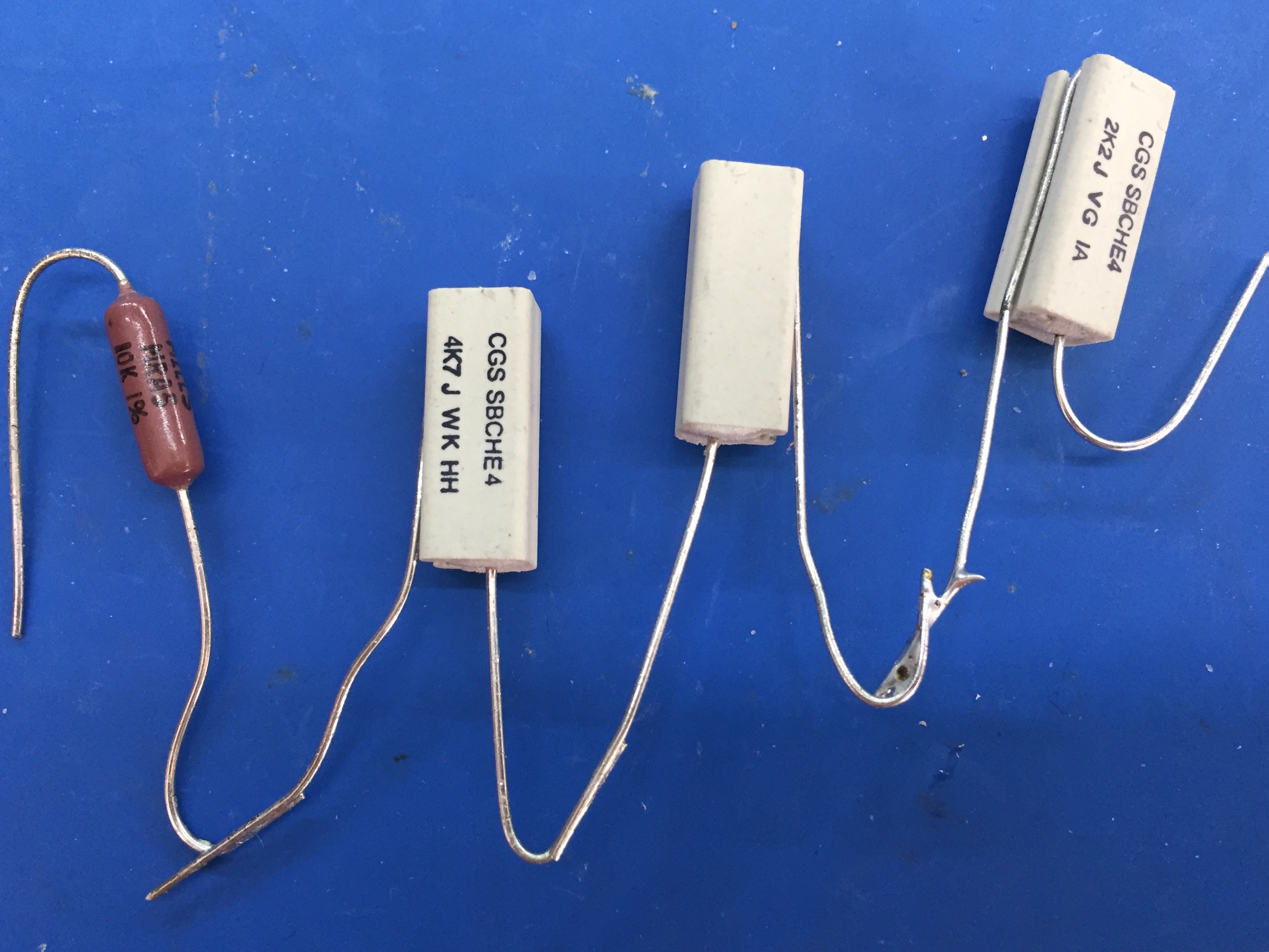
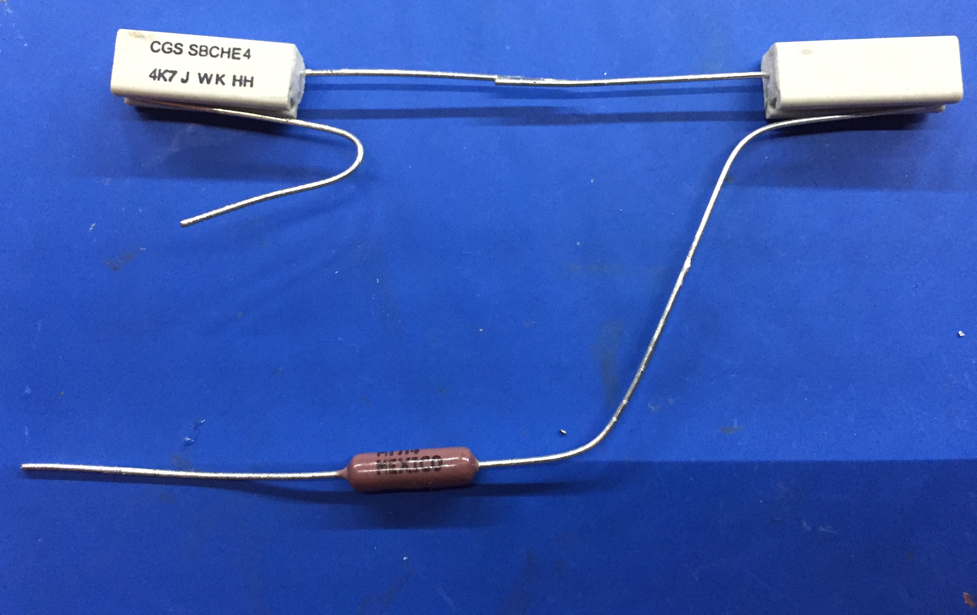
There are some parts on the reverse side too. One important note here: It is obviously important to pay attention to the specs of the parts you order. Wattage on resistors. Voltage and ESR on capacitors. But one that is often overlooked is the voltage rating of the resistors. Typically this is around 100V, however the feedback resistor has pretty much the entire output voltage across it permanently, so that specific resistor is rated to handle it.
An interesting one is the current sense resistor. I ordered some wire wound resistors, which was a mistake because they introduce inductance to the circuit. The non-wire wound resistors worked fine.
I think I over-spec'd the diode!
What followed was a comedy of errors. Firstly, I had the output stage connected the wrong way around. Remember this diagram?
![]()
Those dots are important. I had them the wrong way around. I fixed it by swapping the inputs and presto, I was in business. However, I most definitely was not getting 186V, except with no load (actually 184.6V with no load. Near enough). BTW, this is what my test load looks like:
![]()
Three high power resistors connected in series. I had considered building a test load, but I didn't want to get diverted into yet another project!
I spent the next few weeks changing the values of various parts. One of the key ones turned out to be the frequency setting. I started with a resistor of 24k, which should have given me a frequency of about 600KHz. I gradually reduced it, and as I did so the performance kept improving. I ended up with a resistance of around 47k, which gives a frequency of about 350KHz. At that frequency, varying the other values didn't make much difference. However I noticed that the IRL640 was getting really hot. Apparently LTSpice doesn't model the thermal characteristics of the components. I could actually see the output voltage dropping as it warmed up ('warm up' is an understatement!).
My reasoning was that the Rds(on) of 0.18Ω was just too high, so I searched for a replacement with lower Rds(on) and came up with the IRLI2910. This has an Rds(on) of just 0.026Ω. When I swapped this in to the circuit, it never got warm and my output voltages improved - less power was being dissipated as heat. An added bonus, Infineon have a spice model for it, so I can easily plug it into the simulation.
The values still weren't that great though. Still not getting to 184.6V! While I was taking measurements to calculate efficiency, I just happened to notice that if I measured the input voltage at the board instead of at the power source, it was a full 1V less. My 5V source was a USB wall adapter. With a load, this voltage was dropping to around 4.6V. With the additional 1V drop, this was down to 3.6V! The culprit was one of the leads I was using. I junked it and my performance improved dramatically.
So how was it? These are the values I get from this prototype now, using the IRL640 (which still gets very hot, but that's OK for the brief time I am taking measurements):
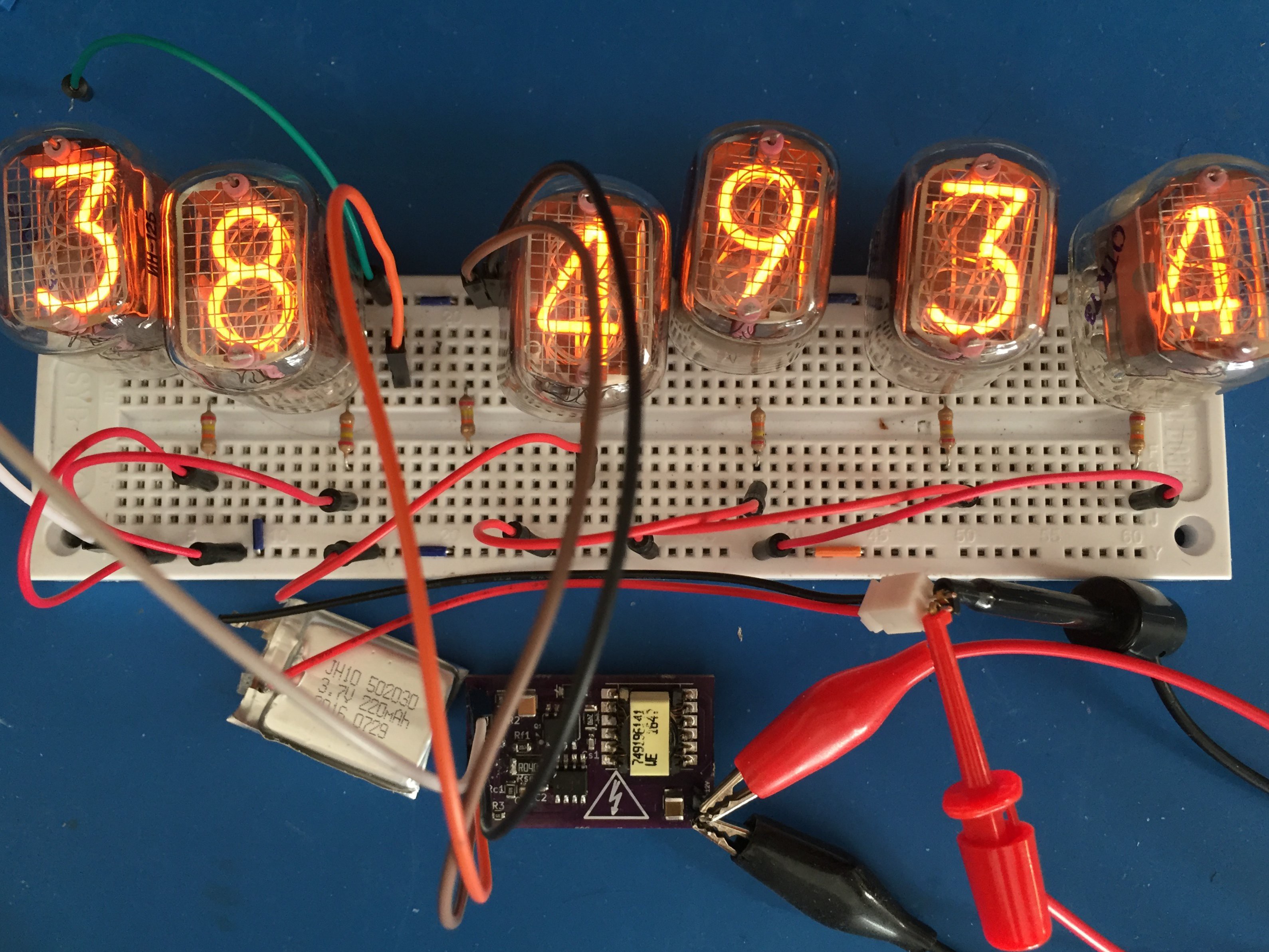
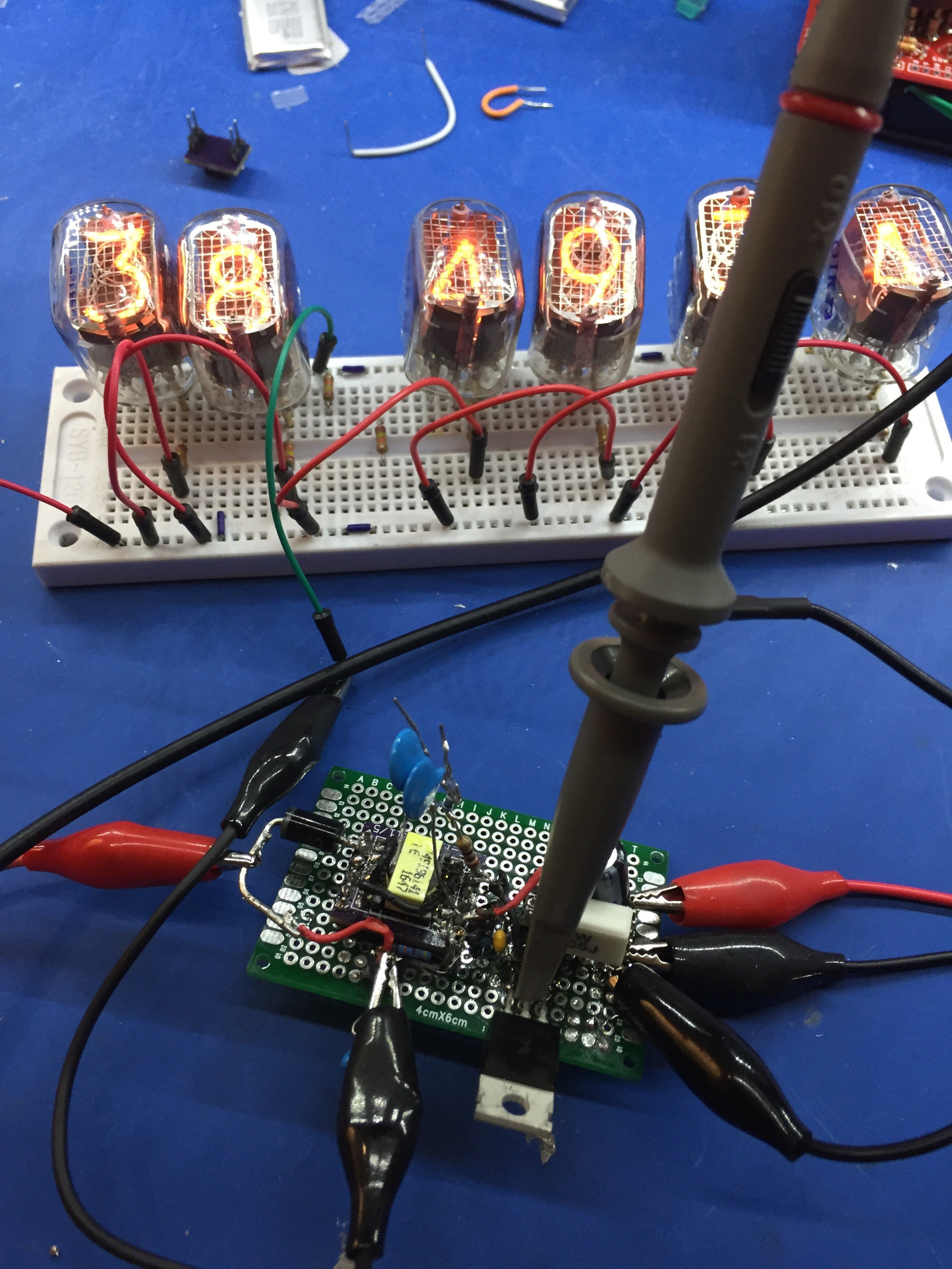
12V in Volts out Current out (mA) Power out (Watts) 20K load 180 9 1.62 15K load 181 12 2.17 10K load 181.5 18 3.267 5V in 20K load 173 8.7 1.5 15K load 141 9.4 1.33 10K load 116 11.6 1.35 3.7V in 20K load 145 7 1 15K load 131 8.7 1.4 10K load 114 11.4 1.3 Well. That isn't too great, but it can light up a bunch of IN-12s - six in this case (this is 5V in, 171V out):
![]()
Yes, I was monitoring the drain voltage on a 'scope. I'll get into that in the next log - you'll have noticed the capacitor/resistor lash-up across the inputs to the transformer, right?
This is 4 tubes at 176V from a LiPo battery. This is pretty much my minimum performance requirement. The whole point of this exercise is to get something that can run a battery powered clock. So I got to there, and with something that I didn't expect to meet the full performance of the LTSpice model, because it was lashed together on perfboard:
![]()
What you can't see is the FET's heatsink glowing red. OK I exaggerate, but it was really hot. This is the IRL640 remember - the IRLI2910 had no such problems and performs better. It was certainly encouraging and worth going on to the next step of designing an actual PCB. But first, that scope output...
-
Refining the Design
10/30/2017 at 00:23 • 0 commentsI'm dealing only with the simulation here. I'll get to actual component selection when I discuss the prototype and the finished board.
Input Voltage
I chose 5V as a target input voltage. I could run the simulation at 12V, but that isn't my target input, that is just something I would like my power supply to be able to handle. I also want it to handle a LiPo battery, so I need to run the simulation at 3.7V too.
However, the big problem with the first simulation is that there is no internal resistance specified for the voltage source. A real voltage source does have an internal resistance, and this causes the input voltage to drop as more current is drawn. I change the simulation to use an IR of 0.5 Ohms. This seemed to produce a realistic drop in the input voltage.
Output Capacitor
The output capacitor (C2) serves to smooth out the ups and downs of the output voltage by storing charge during the on phase of the diode and providing it when it is in the off phase. If the capacitance is too small, the output will have a ripple. If it is too large, it will take too much power to charge. 0.22uF is lower than most designs seem to recommend. I tried up to 1uF in the simulation. The only effect was to lengthen the ramp-up time, so I stuck with 0.22uF.
Capacitors have a resistance called ESR (Equivalent Series Resistance). This affects how quickly it can discharge and, of course, dissipates power. The lower the better. My model used 0.025 Ohms.
Rsense
The transformer model provided by Wurth actually models things like saturation current, so I was intrigued as to how much I could affect the simulation by varying this resistor. I dropped it as low as 0.02 Ohms, which had no effect. I raised it 0.1 Ohms and this completely destroyed the circuit's ability to generate a high voltage. So I stuck with 0.05 Ohms!
Input Capacitor
This capacitor smooths the input voltage by charging while the MOSFET is off and providing power when it is on. Like the output capacitor, you want to have a low ESR so that as much power is delivered as fast as possible to the transformer. I left this value completely alone and defined an ESR of 0.074 Ohms.
Ccomp and Rcomp
And so we come to loop compensation. Do you know what Bode plots are? How about poles? Zeros? Right half planes? No? Me neither. Basically, what these values do is to control how quickly the chip responds to changes in load to keep the voltage constant. If it reacts too quickly the output voltage will jump up and down. If it reacts too slowly, the output voltage might never adjust to the load before the load changes again. I messed with these values. If I increase Ccomp (to say 220nF) the simulation overshoots the target, then drops, then overshoots. etc. If I decrease it, there is a ripple in the output. In other words, 22nF seems about right. Changing the resistance has no noticeable effect.
If you are interested, this is all dealt with in note AN-1286. There is an online bode plot tool here or here. I did try and use the math to calculate the ideal values. I worked through the example in AN-1286 using excel and one of the online bode plot calculators, but my numbers didn't tally with theirs. I would be interested if someone could do this, though it doesn't really affect the actual circuit. I asked the folks over on Neonixie about this. They said 'Just build the prototype!'.
The MOSFET
Finally, the MOSFET. Nick de Smith has some recommendations:
Select the FET for low RDSon, Qg and Coss
So I did. I changed the FET to an IRL640A. Basically, again, we want the MOSFET to consume as little power as possible.
However we need some other characteristics:
- Vds needs to be able take the reflected voltage from the secondary. The IRL640A has a Vdsof 200V!
- Vgs(th) needs to be significantly below the input voltage. This value is the threshold at which the MOSFET starts to turn on. It actually completely turns on at some value above this. The IRL640A has a Vgs(th) of 1 to 2 volts.
It eventually turned out that this wasn't a great choice. We'll get to that.
Sadly, there seems to be no LTSpice model for the IRL640A, so I had to make one using this tool kept at the Yahoo mail group.
Results
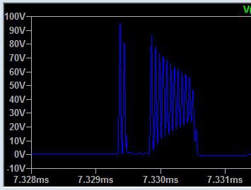
The results aren't much different than the initial circuit. The output voltage curve is pretty much identical. This is the reflected voltage (Vds):
![]()
There's still ringing, but it's a little bit better. Peak voltage is at least below 100V!
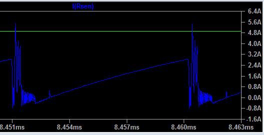
Let's take a look at the current through the primary side:
![]()
By my reading of the Wurth data sheet the current can go up to around 6A before the transformer saturates. So we're good, but there is clearly ringing going on here too.
We'll address that in the next log.
3.7V
If I run this using 3.7V, I get this:
![]()
This is not good! The MOSFET apparently stops switching. The IR of 0.5 Ohms is excessive for a LiPo. It turns out that this was pulling the input voltage below 3V, which is too low for the IC (not sure why this means the MOSFET apparently stays on, but whatever. The internal resistance of a LiPo is typically in the mOhms. Anyway, setting a more realistic IR for the input fixes this problem.
-
LTSpice
10/28/2017 at 03:34 • 0 commentsOh boy, where do you start with LTSpice? That’s precisely the problem I had. It seems like it is purpose built to model power supplies. Perhaps this is a biased point of view though, because that is where I discovered it. However it took me a long time to become comfortable using it - I found it’s interface to be particularly clunky. I’m pretty used to it now though. The one thing I still dislike strongly is how to add new components and sub-circuits to it. And we will need to do that to model my power supply. There is a tutorial here, a dedicated wiki here, and a yahoo group here.
I spent months, literally, simulating my circuit in LTSpice, trying to become comfortable with what each component was doing in the circuit. This is not to say it was difficult, in fact my very first circuits pretty much worked from the start, but past experience had shown me that something that works fine in LTSpice can fail miserably in real life. So I wanted to get comfortable that I had produced the best simulation I could, i.e.:
- Used real-world components rather than ideal components.
- Explored the limits of what the circuit could do in terms of power sources, loads and component variations.
The circuit I ended up using was pretty much lifted straight from the LM3478 datasheet but with a flyback transformer in place of the inductor. TI provide a ton of information about this IC, including how to use it in a flyback converter! You will find a ton of math in these papers. Especially, when it comes to flyback converters, just about every reference you will find is aimed at figuring out what the specification of the transformer should be. This is great if you are going to wind your own transformer. We aren't, we actually want to start with the transformer and work back. I went down the rat hole with these calculations. What I found, in the end, was that most of them don't really matter. The circuit pretty much works out of the box. LTSpice allows you to get close to the right values for the components. A few prototypes let you fine tune it.
What is important is paying attention to the physical characteristics of the board. This was emphasized by Nick de Smith's design for a MAX1771 based Nixie power supply, and rammed home by looking at the datasheet for the LM3478 evaluation board (like I said, TI provide a ton of information about this IC).
Anyway, I digress.
The first thing I did was to download the spice models for the LM3478 and the Wurth Flex Transformers and set them up for LTSpice. Then just forged ahead and entered the circuit. It looks like this:
![]()
- U1 is the LM3478.
- U2 is the transformer.
- D1 is the output diode. I wasn't picky, I just chose one from the LTSpice standard parts that has a breakdown voltage of around 350V.
- R2 and R3 together set the output voltage. The LM3478 tries to keep the FB pin at 1.26 volts (typically). So the output here should be:
Or 186V (typically).
- Rload would be nixies in a clock. Using 10K here means we are draining 18.6mA. That would be 3mA each for a clock with six tubes.
- V1 is the input voltage, which I have set to 5V.
- Rfreq sets the frequency of the PWM signal being placed on the gate of the MOSFET.
- That MOSFET (AON6242) was just selected from the standard set of MOSFETs that LTSpice knows about. It has a 60V Vds - i.e. it can withstand 60V across the drain-source. 60V should be OK, because we are keeping the output voltage below 200V. So as a rough first estimate, we would expect the maximum voltage on that side of the transformer to be at most 40V. This is because the turns ratio of the transformer is 1:5. So 200/5 is 40.
- Ccomp and Rcomp control the loop compensation - I will get into that later. These values will do for now.
- R4 is the current sense resistor: The LM3478 monitors this and will cut off the MOSFET if the current goes to high. We want the current to stay below the saturation current of the transformer. 0.05 Ohms will do for now.
- The pieces of text that start with a period are LTSpice directives. The first sets up some simulation parameters. The second includes the LM3478 library. The third configures the transformer model.
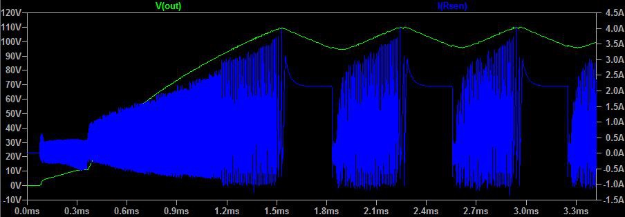
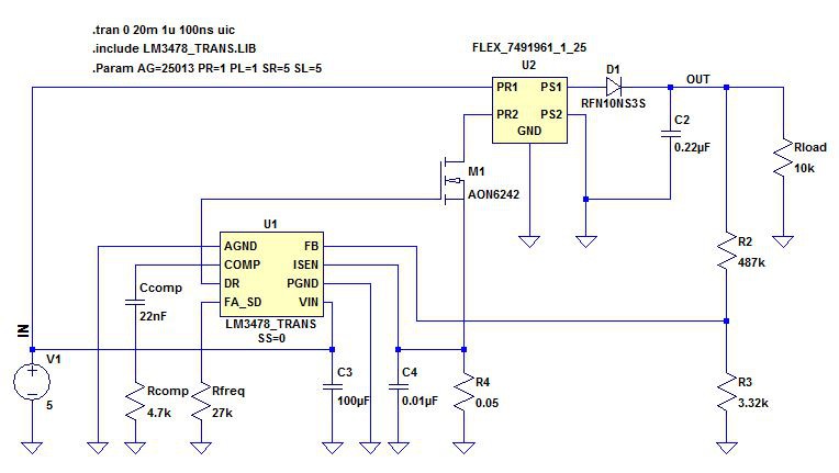
So how does it do? Here is the output voltage graph:
![]()
So it gets up to around 180V, which is within the margin of error for the FB voltage monitor (remember 1.26V was typical).
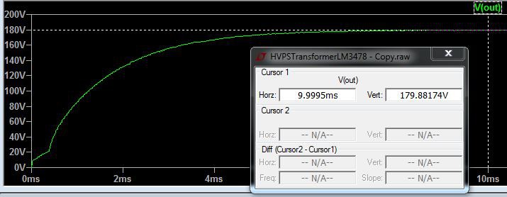
Let's have a look at the Gate of the MOSFET:
![]()
You can see that it is using about a 66% duty cycle at a frequency of around 108KHz.
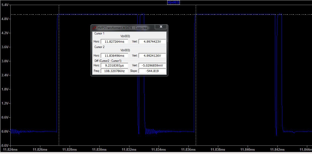
Now let's look at the Vds (the voltage presented to the drain of the MOSFET):
![]()
OK. That doesn't look so good. We've got a nice square wave at the gate and an unholy mess on the drain. Look at the peak voltage. 120V. Way beyond the 60V our MOSFET is rated for. This is an example of ringing. It is caused by what are called parasitic inductances and capacitances in the circuit. In this case it is caused by capacitance in the MOSFET and leakage inductance in the transformer.
I will get into all of this later, but right off the bat, we seem to have a circuit that basically works. All we need to do is adjust the components a little. Right? Right?
-
Theory of Operation
10/28/2017 at 02:16 • 0 commentsAs mentioned earlier, the basic idea of a boost converter is to use the collapsing field in an inductor to generate a large voltage. To do this you need to be able to turn the current on and off. This is done using a transistor, usually a MOSFET.
This is the typical diagram used to explain this:
![]()
When the switch is closed, the current flows through the switch. When it is open, the field in the inductor collapses and generates an additional voltage in the same direction as that from the power source. The current can't flow through the switch, so it flows through the load. The capacitor provides current to the load while the switch is closed. The diode prevents this current from flowing back in to the inductor. After startup the diode blocks current flowing from the left side of the circuit while the switch is closed because the voltage on the right side is greater. This page gives one the best explanation of this I have seen.
As stated earlier, a flyback converter essentially replaces the inductor with a transformer, like this:
![]()
The rest is the same. This gives us two advantages:
- We get the voltage multiplying effect of the transformer (at the expense of current, conservation of energy and all that).
- The output is isolated from the input. With a boost converter, if the switch is left open the output voltage will be the same as the input voltage. Which is interesting, but not why we want to use one.
Generally, you want the switch to be closed longer than it is open. The longer it is closed, the more energy is pumped in to the magnetic field of the inductor, so the more power will come back out in the form of voltage (give that the current is constant), once we open the switch. This ratio of on to off is called the duty cycle. An 80% duty cycle means that the switch is closed 80% of the time. This on-off mechanism is also called PWM (Pulse Width Modulation). It is a square(ish) wave. In most documentation about boost converters, they will talk about small duty cycles - say 60%. In Nixie power supplies, 90% is not uncommon because we want to boost the voltage a lot!
In addition to this ratio, there is the period of the wave. After a certain amount of time, we will have pumped as much energy in to the inductor as it can take - the magnetic field won't get any stronger. There is no point pumping in any more. The larger the inductance, the more energy we can pump in. Unfortunately, large inductance and large physical size go hand in hand, and we want a small inductor. This effectively means that we need to switch the current faster so as to avoid saturating the inductor.
So smaller inductor => higher frequency.
If the frequency gets too high, circuits start behaving oddly, so we don't want to go too high. 600KHz seems like a recommended upper limit. Of course this also puts limits on how small the inductor can be.
This is all relevant to our design - we will be adjusting all of these things to try and come up with the best solution we can, given the actual products available to us.
-
Switching Controller
10/27/2017 at 22:02 • 0 commentsApart from the transformer, I need to find a suitable switching controller. The key to a good power supply is that it produces a stable output. The keyword here is 'regulated'. To produce a regulated voltage, the power supply needs to be able to adjust to the load being placed on it (or, I guess, be so powerful that any load you put on it is negligible). There are quite a lot of tutorials on the internet for building Nixie power supplies, including some that use transformers (none that use an off-the-shelf transformer, hence this little project) and most of them use a switching controller. Here are some:
- Coin cell-powered supply. I built this one. It isn't regulated, but it uses a transformer. I learn't a lot about batteries building this :)
- A regular boost converter. This one has invaluable advice about the actual engineering of building something that works. It uses a regular inductor, not a transformer.
- Obsolete Time Lite, right here on Hackaday. This actually uses a transformer. I was really excited! But I couldn't figure out which transformer, and the project seems to have been abandoned. My big takeaway from this was the specific controller it used.
There are many more, and I'll provide a list from my bookmarks at the end, but my point in listing these is to give a sample that use different controllers. So, I created a spreadsheet of some of the controllers that included a list of specific features. This enabled me to focus on a few that had everything that I wanted. My key requirements were:
- Needed to operate on an input voltage of 3V-12V.
- Needed to be able to produce a high duty cycle, say 90%
- Needed to be able to drive an external MOSFET - rather than having a built-in transistor.
- Needed to have a way of enabling and disabling the output.
- Needed to draw a small amount of current in disabled mode.
I tried the MC34063 first, even though it didn't have a way to disable it - it is widely used and I could get an LTSpice model for it (modelling is a big part of this, as will become apparent).
I tried the LM3478 next, as used in Obsolete Time Lite. This is as far as I got! This made it all the way into my finished supply.
Next up would have been the MAX1771. Everyone swears by it. Many apparently swear at it! It is allegedly very finicky.
After that would have been the LT1619. In many ways this seems like the ideal choice, I just never got this far - the LM3478 seems to work just fine. Plus I didn't want to be swayed by what the excellent Taylor Edge HVPS uses. Part of the reason for this project is to produce my own power supply.
All of these companies sent me samples. Something I am very grateful for.
Nixie Tube Power Supply
A flexible power supply for Nixie tubes. Input voltage can be from 3V to 12V. Output up to 200V. It uses commercially available transformers