Objective :
The objective of this project is to implement an android game named "Archery Black" on LPC2148 microcontroller using Nokia 5110 LCD screen. Archery Black is a simple and easy to play game. The simple and challenging nature of this game makes us to play it more and more.
Components used:
1. LPC2148 microcontroller
2. Nokia 5110 LCD
Description:
1. LPC2148 microcontroller is the widely used IC from ARM-7 family. Here, in our project, the following features of PPC2148 are used:
SPI Protocol
Timer
Vectored Interrupts
Frame Buffer
EEPROM
Buzzer
Onboard LCD screen
SPI Protocol :
SPI is a masrer-slave protocol, one device acts as the bus mster while any number of devices can act as slaves. In this project, LPC2148 is the master device and Nokia 5110 acts as slave. SPI is a serial communication protocol that means all the data going in or out is synchronized by a clock. SPI device has separate lines for data in and data out.
All SPI based communication happens over 4 lines named MOSI, MISO, SCK, SS.
MOSI - Master Out Slave In (master device sends data over this line)
MISO - Master In Slave out (master device accepts data over this line)
SCK - Serial clock (generated by bus master)
SS - Slave select (Useful in the case of multiple slaves)
How Nokia 5110 is connected to these ports is explained in the later sections.
2. Nokia 5110 is a 48x84 LCD screen. Its driver is called "PCD8544". The PCD8544 is a low power CMOS LCD controller/driver, designed to drive a graphic display of 48 rows and 84 columns. All necessary functions for the display are provided in a single chip, including on-chip generation of LCD supply and bias voltages, resulting in a minimum of external components and low power consumption. The PCD8544 interfaces to microcontrollers through a serial bus interface. The PCD8544 is manufactured in n-well CMOS technology. Here is the block diagram of PCD8544:
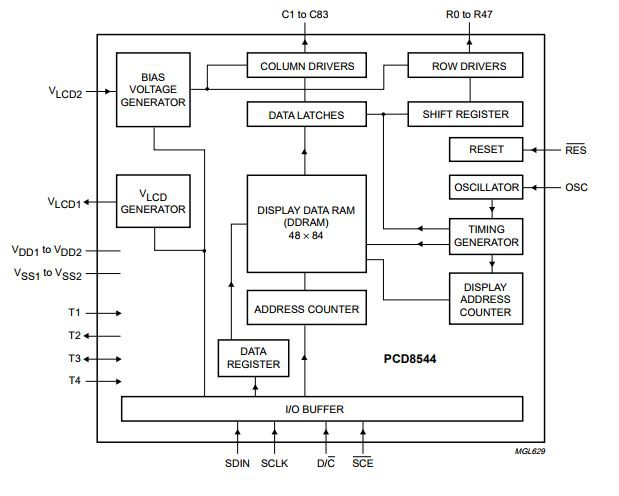
There are 8 pins accessible from outside, details of them are given below:
(i) SDIN: SERIAL DATA LINE
Input for the data line.
(ii) SCLK: SERIAL CLOCK LINE
Input for the clock signal: 0.0 to 4.0 Mbits/s.
(iii) D/C: MODE SELECT
Input to select either command/address or data input.
(iv) SCE: CHIP ENABLE
The enable pin allows data to be clocked in. The signal is active LOW.
(v) RES: RESET This signal will reset the device and must be applied to properly initialize the chip. The signal is active LOW.
(vi) VCC: This provides supply voltage to the device. The LCD works on 3.3 V.
(vii) GND
(viii) BL: This pin is to enable the backlight of LCD. It should be connected to VCC.
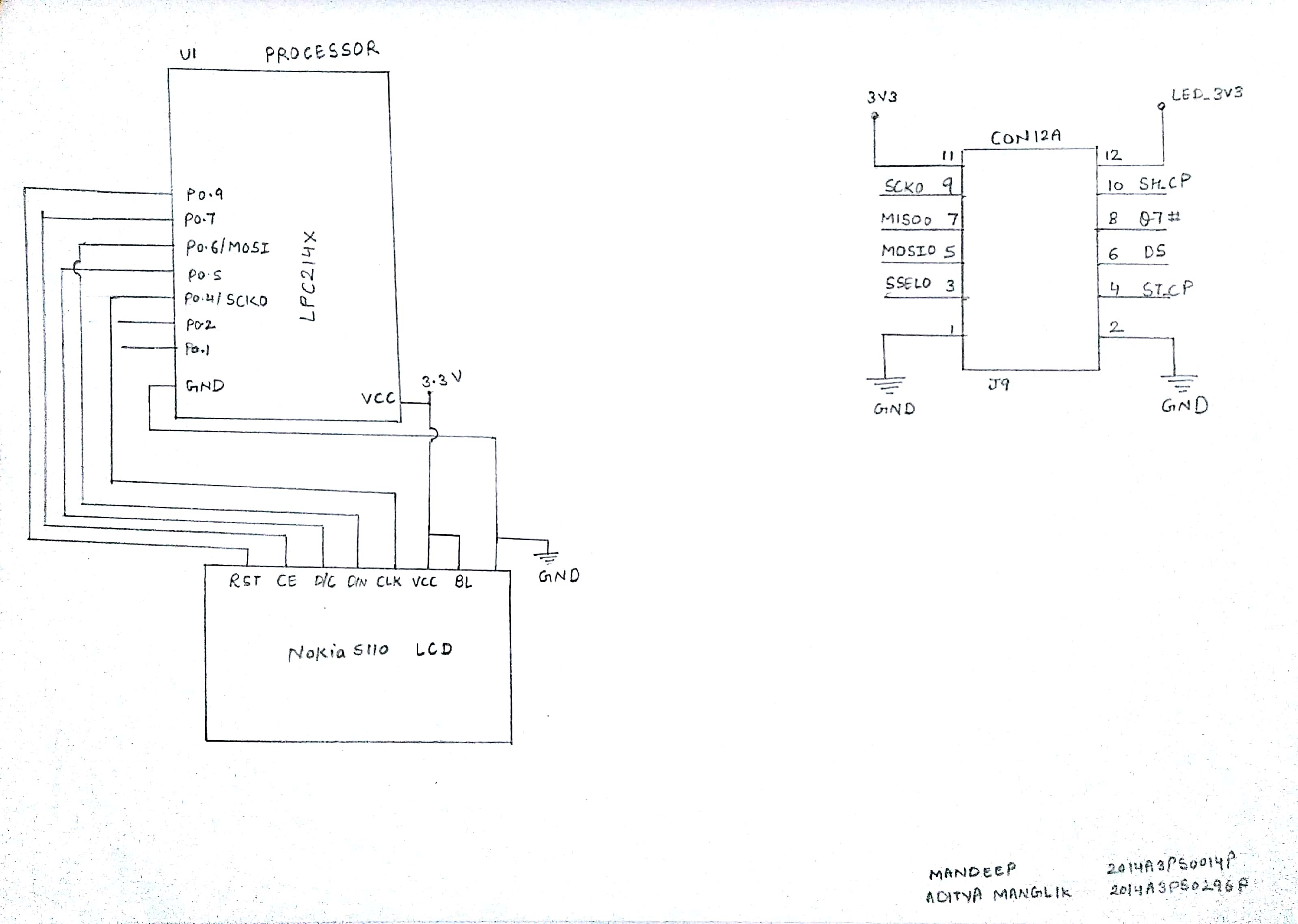
The below figure describes the connection between PLC2148 and Nokia 5110 LCD:
 Marcrbarker
 Kuldeep Singh Dhaka
 Krists
 Blecky