 arief ibrahim adha
Specifications
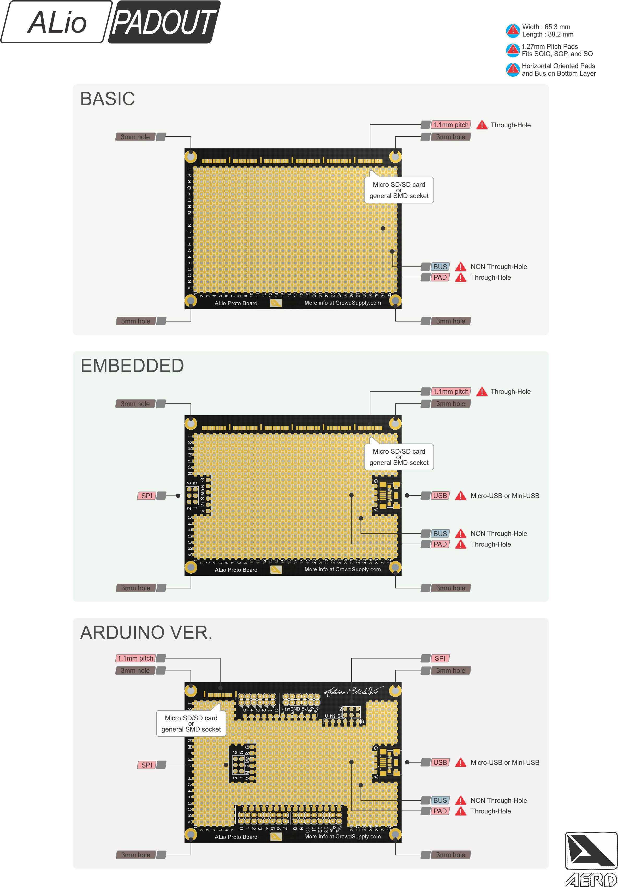
- Size: L x W x H : 88.2 mm x 65.3 mm x 1 mm
- PCB : FR4 0.8 mm
- Finishing : HASL-lead
- Finished copper: 1 Oz Cu with black masking and white silkscreen.
Product Features
- Fits SMD and PTH components at the same time.
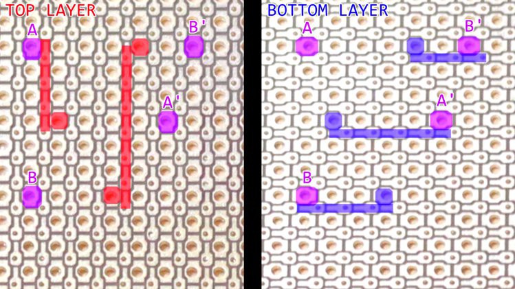
- Has a double-layer BUS for wire-free connections.
- Has a Micro-SD/SD card breakout or any general SMD sockets.
- Has an SPI break out pad for some variant.
- Has a 2-in-1 micro-USB and mini-USB pad for some variant.
- Open source design.
- Large prototyping area.
- No more SOIC-break out boards needed, this board fits all SOIC, SOP, and SO type ICs.

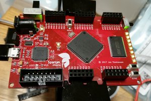
 Jon Thomasson
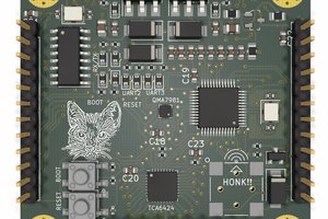
 WingTechCorner
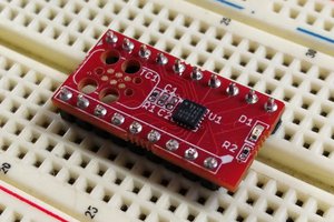
 Parker
 Neven Boyanov
How did you make those "padout" diagrams? I always see development board pinout diagrams in that exact style, but I've never been able to find out what tool everyone uses to make them.