Here is what I know from the device:
- MCU: STM32F102C8
- NFC transceiver: NXP PN512 (http://www.nxp.com/documents/data_sheet/PN512.pdf)
- It shows up as a mass storage device (http://www.st.com/st-web-ui/static/active/en/resource/technical/document/datasheet/CD00210831.pdf)
- VID:PID: c251:1c03 Keil Software, Inc.
- lsusb verbose output: https://db.tt/NPams7kk
The lsusb information reveals that the firmware is built using the KEIL tools.
It might hava a bootloading capability, I will look around the KEIL application notes around the USB mass storage devices and bootloaders category.
Hardware info:
The device is made from two PCBs. A CR2450 battery is placed between them.
MCU board
This is a 2 layer PCB with the following markings:
- SK14
- SZ-M
- RFIdea STM NFC v 3.1.1
Components:
- STM32
- 2 LEDS:
- LED1 (red): connected to PB13 through a 100 Ohm resistor
- LED2 (green): connected to PB14 through a 100 Ohm resistor
- some passive components
- a clock oscillator connected to the PC14-PC15
- a 12 MHz oscillator connected to PD0 (OSC_IN)
- J1 switch is a reset switch (pulls the nRST pin to GND) this button is hidden from the user but it could be accessed through a hole.
- J3: (contact exchange button): pulling to VDD connected to PB10
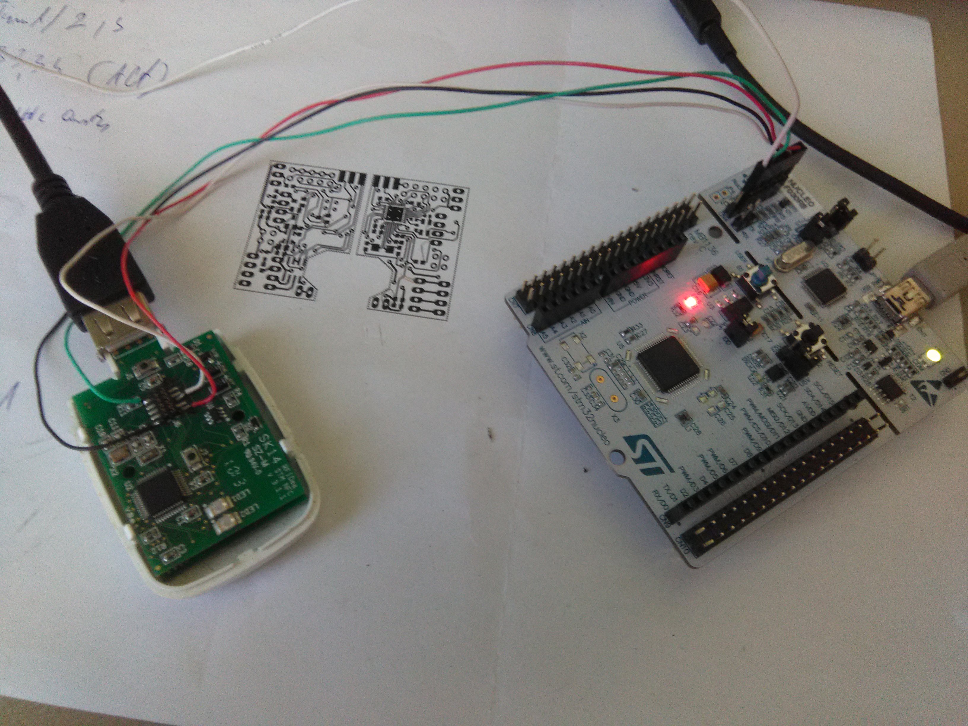
- J6: JTAG connector. Pinout (1 and 10 pins next to the J6 text on the silkscreen)
1: VCC
2:
3: PA14 JTCK
4: PA15 JTDI
5: PB3 JTDO
6: PA13 JTMS
7: PB4 nJTRST
8:
9:
10: GND
RF board
This is a least three layer PCB (have one inner ground plane under the RF area) includes the follwing markings:
- SK14
- SZ-2D
- NFC by RFIDea v 3.1.1
The PCB populated with the PN512, a 27.12MHz oscillator, the interboard connector, and a bunch of passive components.
Interconnect connector pinout (see pin1 marking on the photo).
1: PN512 D7 (UART mode TX) - SMT32 PA3 (USART2 RX)
2: PN512 D6 - NC
3: PN512 ALE (UART mode RX) - STM32 PA2 (USART2 TX)
4: PN512 TVDD, SVDD, AVDD - STM32 VDD
5: PN512 VBAT - STM32 VBAT
6: PN512 A0 - GND (battery GND)
7: PN512 NRSTPD - STM32 PB12
8: PN512 D5 - NC
9: PN512 IRQ - NC
10: NC - NC
The PN512 A0 pin is permanently tied to GND. According to the PN512 datasheet it means that it uses UART for communication through the ALE (RX) the D7 (TX) and the D6 (MX) and the D5 (DTRQ) lines. This correlates with the connection pins with the STM32. So I have an UART-NFC converter. Cool. Time to look after some PN512 handling libraries.
 Miklos Marton
 gertux
 deʃhipu

 benjaminaigner
 Benjamin Vernoux