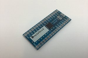
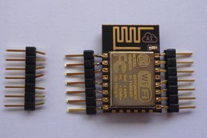
The breakout board has various bits and pieces on it. The stuff that's important to you would be the power regulator, the pin headers, and the two optional solder bridges.
First off is the pinout. For power/serial/SPI/ADC/reset this is pretty clear - every pin for these is silkscreened. For the four GPIO pins that are broken out, it's a bit less clear as I didn't have enough silkscreen room for every pin. Each GPIO pin is labelled with its NodeMCU pin #, as well as the raw GPIO pin number. To each side of the GPIO pin is a power pin. These power pins are tied to VIN, and not VCC, so keep that in mind. Two of the GPIO pins can be used as I2C, and all four of them have PWM capability.
Second, the solder bridges. There are two.
- The DPSLP bridge ties D0/GPIO16 to the RESET pin. This allows the ESP8266 to wake itself up from deep sleep via the RTC module. Keep in mind this means that you cannot use this GPIO pin for anything else!
- The VCC=VIN bridge bypasses the NCP114 linear regulator. If you supply the board with 3.3v, then you don't need a regulator and you can just bridge this. I would still recommend using at least one of the two capacitors in order to maintain good power quality.
The NCP114 regulator is not meant to provide power to peripheral devices. It is sized to comfortably power the ESP8266.
The FLASH and RESET tactile switches are positioned and sized so that they are reasonably possible to press with a single thumb, or with both index fingers if you hold the breakout board with the antenna pointing at your head, ESP facing toward your chest.
 Sukasa
 Ben Lim

 B K
B K
 Clovis Fritzen