Close
0%
0%

Bench Power Supply

Designing an open source, modular bench power supply to rule them all.

Similar projects worth following
This is a design for an open source, modular bench power supply with enough features to compete with the mid-range commercial units in the $1000-ish range. This project includes features such as software calibration, programmatic control via USB Raw HID, etc. In its simplest form, it is very affordable, but can be easily scaled up to a larger, more powerful unit.

HaD Prize 2015 Questions:

What problem does this solve? Just about every hacker in the world needs a good power source. While re-commissioning an ATX supply is a rite of passage, these supplies are somewhat limited in what they can do. They tend to only have 4 fixed voltages (12, 5, 3.3, and -12); futhermore, you need to use multimeters to determine actual voltage / current output. There is no current limiting (if you short the rails the supply will turn off, but it will happily supply multiple amps of current up to that point). This project attempts to solve these problems in an economical fashion.

How does it solve the problem? This design is for a digitally controlled and calibrated multi-channel power supply with current limiting. It lets you set the voltage on each channel independently anywhere from 0 to 12V (or 0 to -12V for the negative channels), with configurable current limiting on each channel, and actual voltage / current display. It supports USB control from a PC (using RawHID packets) for calibration and automated setpoints / logging.

How to use it? Set the voltage / max current setpoints for the circuit under test (e.g. 5v, 500mA if testing a USB powered device). Plug in the device. Watch the voltage / current readouts to see how much current is being drawn.

License: As with all my other projects on HaD, this is released under a Creative Commons Attribution license. Make it, change it, sell it - just have fun while doing it and link back to my project so that others can benefit as well! Everything that I created while designing it - the AVR source code, KiCad source + Gerbers, Enclosure plans (QCad .dxf), simulations, etc are all available on Github.

Project Overview:

Some requirements of this project:

  • Modular power supply from 1 to 6 channels (I have implemented 4 channels: 3 positive, and 1 negative)
  • Each channel can independently be set from 0-12V (for positive channels) or -12-0V (for negative channels), and the output can go all the way to 0 (which is not the case with most DIY power supplies).
  • Configurable set points for voltage and max current for each channel
  • Actual readings for voltage and current for each channel
  • Low cost - it's not as cheap as scrapping an ATX power supply (which is what I used to use), but the extra features such as current limiting should more than make up the extra cost.
  • Active (fan) cooling combined with heat sinks to support sustained high current loads
  • USB control (voltage and current set points), logging of actual voltage / current readings, and computer-based calibration.
  • The ability to use potentiometers for voltage / current set points instead of a microcontroller, if desired (each channel has four analog I/Os: Voltage and Current setpoints, and Voltage and Current sense outputs. All of these are in the range of 0-5V, allowing easy control from either a potentiometer or a DAC.

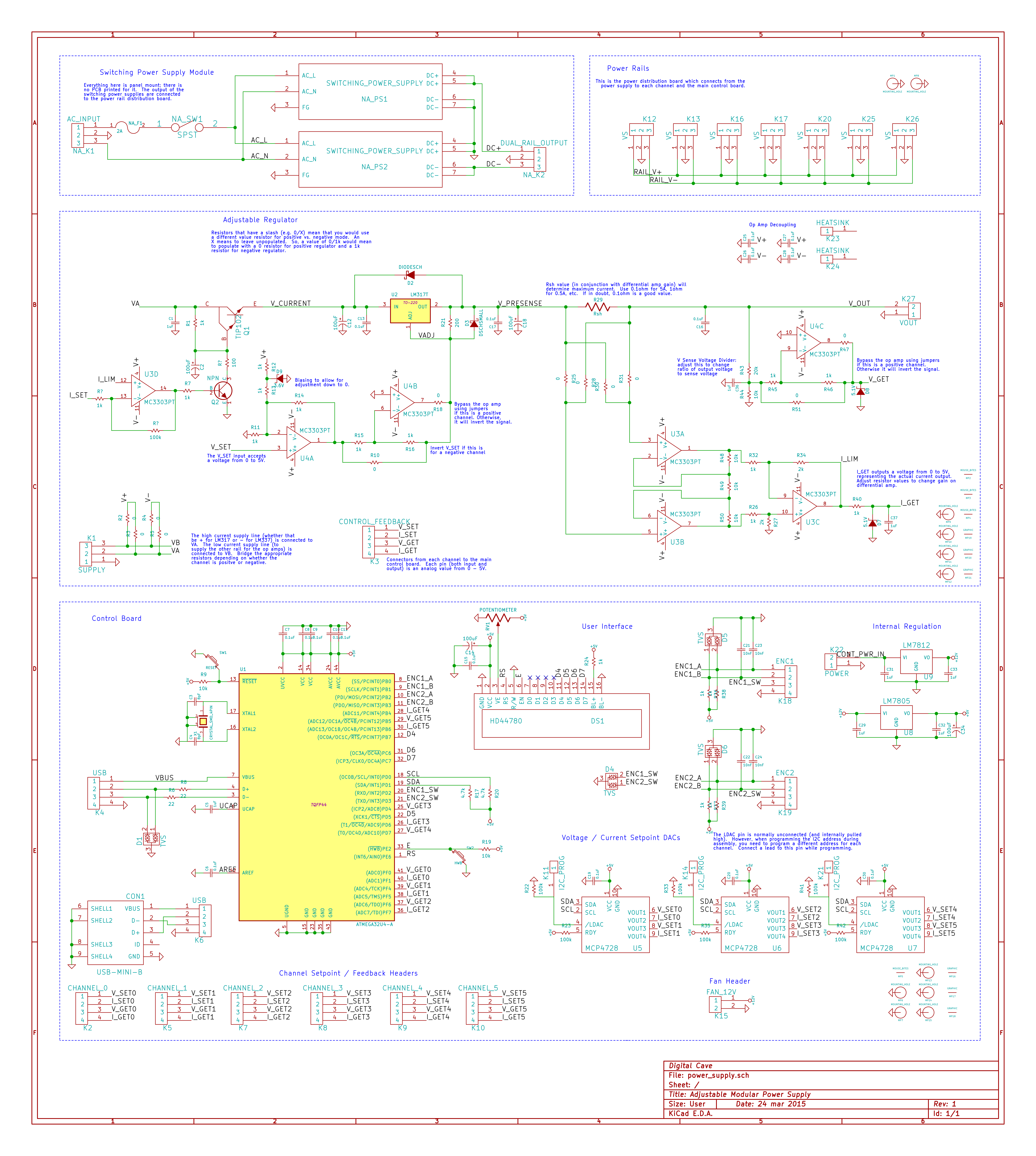
The design has two distinct parts: the power channels, which are controlled by an analog value from 0 - 5v for both voltage setpoint and current limit and which output a value from 0 - 5v to indicate the actual voltage / current, and the control board which can generate said setpoints and read the actual values.

The design uses mostly basic components, with each channel based on the TI LM338 / LM337 with op amps for control. The digital control board runs an Atmel ATMega32u4, and generates the analog setpoints via the Microchip MCP4728 I2C DAC. The same board can be used for either positive or negative output depending on which optional components are populated. (For instance, you would use either an LM338 for positive, or an LM337 for negative; you would use a NPN transistor for current limiting on a negative channel, and a PNP for positive channels; there are different arrangements of 0-ohm resistors used as jumpers to configure positive or negative modes). If you choose to not bother with current limiting you can eliminate the transistor plus an op amp with supporting passive components.

The BOM costs break down as...

Read more »

  • 1 × TI LM338 (Positive) / LM337 (Negative) TO-220 Footprint
  • 1 × TIP107 (Positive) / TIP102 (Negative) TO-220 Footprint
  • 1 × 0.1 Ohm 1% Resistor SMD 2512 Footprint
  • 2 × Ohmite FA-T220-64E Heat Sink
  • 2 × MC3303PT Quad Op Amp TSSOP-14 Footprint

View all 66 components

  • Software Changes

    The Big One08/30/2019 at 22:25 4 comments

    In case anyone else has made one of these, I have recently made some software changes.  The biggest new feature is that calibration is supported directly from the power supply - no connection to a computer needed.  The reason for this is that I have had nothing but problems with the RawHID Python support on Linux and OSX; setting it up was nearly impossible, and if you did manage to get it installed (with custom compiled code) it would just segfault when you try writing stuff.  After many hours of debugging it, I gave up.

    In addition to adding calibration, I did some code cleanup, updated the code to use my latest build scripts and toolchain, and fixed some minor bugs that I had never bothered fixing before.

    The latest code is on my github page: https://github.com/thebiguno/microcontroller-projects/tree/master/projects/power_supply/avr

  • 6 Months Later...

    The Big One12/24/2015 at 07:54 3 comments

    My power supply has been completed for about 6 months now. I cannot begin to explain how nice it is to have a real power supply; I wish that I had obtained one years ago! For anyone who is on the fence about a real power supply vs. a hacked ATX job, go for the real one, even if it costs a bit more time / money.

    I find that I am using this supply all the time; just today, for instance, I was debugging a power supply issue on my Drum Master board (I have a 3.3v linear regulator which is supposed to source up to 250 mA, but which is browning out when I try to write to the SPI flash chip). By using my power supply in place of the wall wart, I was able to determine what was actually happening and how to fix it (spoiler alert: my wall wart's voltage was too high, and thus the linear regulator had to dissipate too much heat and would go into thermal shutdown). Could I have figured this out without an adjustable power supply with actual current readings? Of course. But it would have been harder.

    Anyway, 6 months on, and I am loving it.

    Merry Christmas, all!

  • Semifinals Video Added

    The Big One09/17/2015 at 01:46 0 comments

    I have just added the Hackaday Prize Semifinalist Video. This shows the power supply in action, powering another WIP project that I am currently working on. I also discuss some of the other features (USB calibration and control, etc) and some of the shortcomings of the design (requires a dual supply; difficult to isolate).

  • Free Adjustable Dummy Load

    The Big One08/23/2015 at 01:24 2 comments

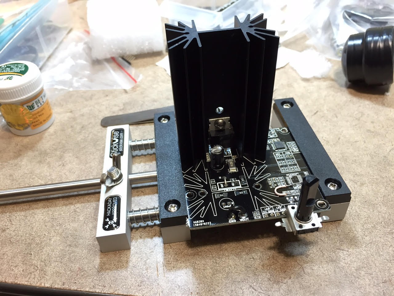
    For those who have ordered the PCBs, you probably have a bunch of boards left over. Rather than just let them accumulate dust in your desk, you can use one of the channels as an adjustable dummy load. It's not the best dummy load, as it was not designed specifically for it, but it does the job decently.

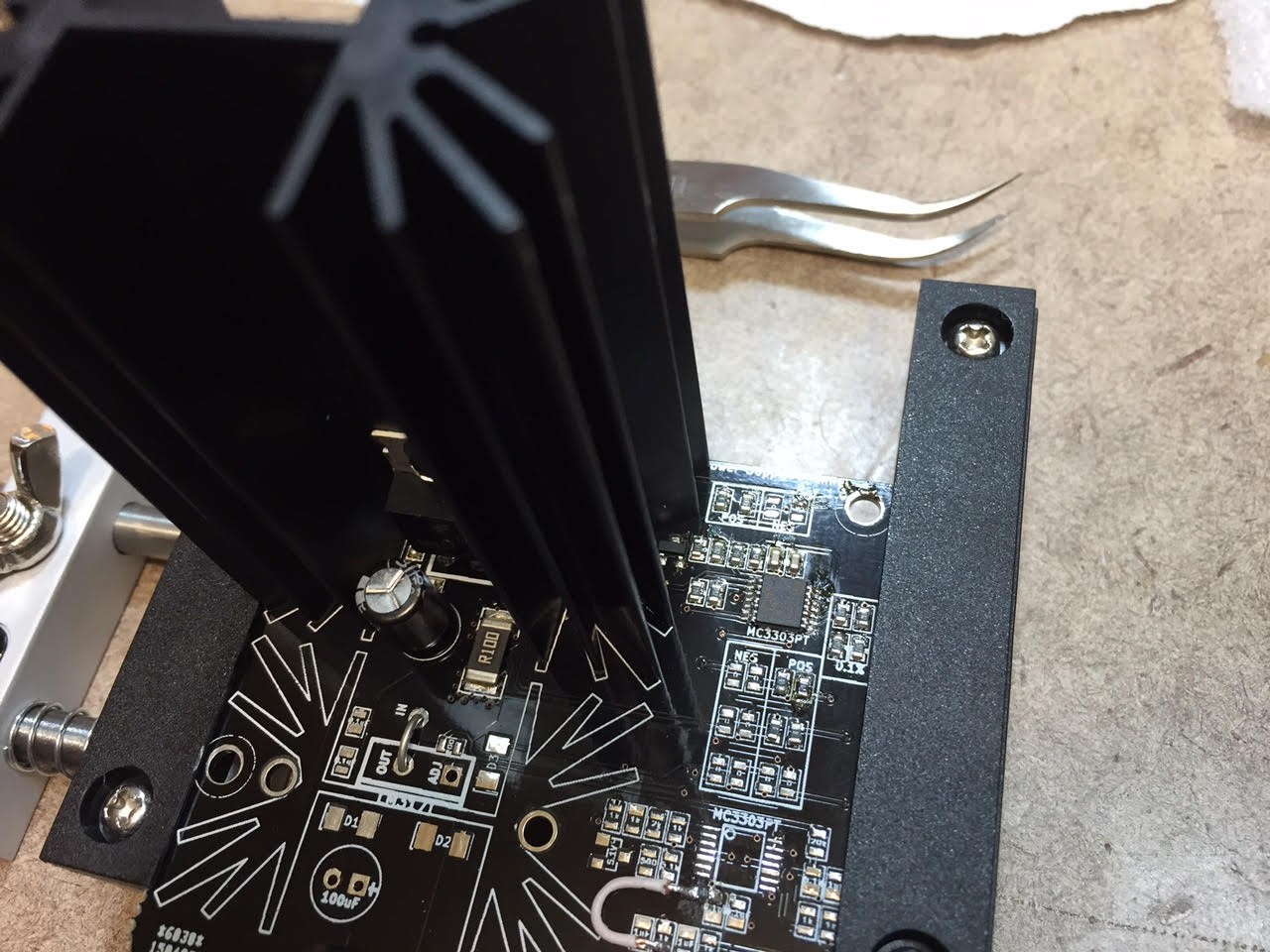
    Basically, you just need to populate the top of the board and add a few jumper wires. Place a jumper between OUT and IN on the voltage regulator chip, and between GND and VOUT at the very bottom. Just as with the power supply channel, you can control the current by applying a voltage on the I SET pin. The lower the voltage the less current will pass. If you use the recommended component values, it will allow for 5v I Set = 5A current. I put a potentiometer on this pin to let me easily control it, but you could also use a DAC or something.

    To use it, you plug in the power supply under test to VA / GND, and supply a negative voltage (I use one equal to VA in magnitude) to VB. (Yeah, it's annoying that you need to provide a dual supply for a dummy load... but that's the way I designed the power supply.)

    If you wanted to improve on things a bit, you could not solder on the top 0 ohm resistors, and instead connect the logic supply (+/-/GND) to those pads; you can then connect the power supply under load to the VA / GND pins. This should give better results since the logic supply is separate from the main supply. Take a look at the PCB layout to see exactly where to solder things...

    Enjoy!

  • Other Makers

    The Big One08/18/2015 at 15:00 1 comment

    To my knowledge there are currently 4 people attempting to make this (at least I can see that 4 people have ordered the Rev 1.0 boards from DirtyPCBs). I have no idea who (if anyone) has attempted to use the new Rev 1.1 gerbers I have posted a few days ago.

    Please let me know if / when you get this working, I would be very interested to see other's versions (especially if you do your own enclosures, but even if you just do it as a bare PCB I would love to see it!)

    Cheers

  • Rev 1.1 Gerbers

    The Big One08/13/2015 at 16:06 0 comments

    If you want to make this yourself, please use the Rev 1.1 gerbers, available on github. This fixes the issues in the Rev 1.0 board, and should make for a smoother experience overall.

  • Project Completed

    The Big One06/18/2015 at 03:32 2 comments

    Yesterday I put the final touches on the wooden case. Everything has come together wonderfully, and just under 6 months of work has paid off:

    Read more »

  • Almost There...

    The Big One06/16/2015 at 15:21 0 comments

    The past week or two has been very busy and productive, although I have not posted many updates. Most of the work has been related to the case.

    I have always planned for the case to be made of wood. I had a rough idea of the design (two sides + top, joined with finger joints, sliding down over the aluminum faceplates and secured with screws on the sides). In order to do this, though, I needed to make some tools... read more for details and to see all sorts of pictures!

    Read more »

  • First Real-World Use

    The Big One06/10/2015 at 05:04 0 comments

    Even though it is not quite finished, I used my power supply for the first time today (the first time for a real project, not just testing the supply itself). I was powering on an H-Bridge circuit for the first time, and wanted to a) ensure that it didn't suck too much current if there was a bug, b) see how much current was being drawn. It performed both tasks flawlessly (and for the record, there was in fact a problem with the H-Bridge board, so current limiting came in handy!

  • Multi Point Calibration Working

    The Big One06/09/2015 at 16:56 0 comments

    Over the weekend I have implemented multi point calibration. I currently use 8 calibration points, which seems to work just fine. I use linear interpolation to get calibration values between the calibration points. Testing shows that things are working quite well. Current limiting is working, and accurate down to less than 20mA (I can even plug an LED directly into the power supply outputs without it blowing up!)

    I also added the ability to set startup voltage / current limiting on a per-channel basis. This is configured via the calibration script (run on the computer, talking to the power supply over USB Raw HID).

    I will post a demo video when I get the chance, although that may not be for a few days given my workload right now...

View all 49 project logs

  • 1
    Step 1

    PCB Rev 1.0 Errata:

    1. Diode D3 is reversed in the board silkscreen. Place it backwards (opposite of what is shown) for a positive supply, and normal (as shown on the silk screen) for a negative supply. Rev 1.1 has been changed to be correct.
    2. Crystal X1 is rotated 90 degrees on the board silkscreen. Instead of placing it with the long side oriented up / down, place it with the long side oriented left / right. Rev 1.1 has been changed to be correct.
    3. There is a problem with the ISP circuit, which prevents you from programming a bootloader (or flashing fuses, or doing anything with the ISP) when the AVR plus all components are on the board. Please program the bootloader and flash fuses (using the script in power_supply/bootloader/program.sh) prior to soldering the entire circuit. You can do this in one of two ways: either program the chip prior to placement (if you have some sort of removable TQFP socket), or solder the AVR + crystal + 8pF caps and then program it, and only once the bootloader is programmed do you finish soldering the rest of the circuit. UPDATE: In the latest iteration of the Rev 1 controller, I have decided to not solder the encoder pullups / caps / TVS directly to the board; rather, I will solder it to the encoders themselves (which can then be detached from the board using the jumper cables). This allows ISP to work properly when the encoders are unplugged. Rev 1.1 has been changed to have jumpers to disconnect the encoders, so the supporting hardware can just stay on the board.
    4. The current limiting LED indicator light does not turn on properly. Current limiting works, but the indicator light does not. To fix it, connect pin 6 of op amp U2 to a -3v source rather than GND. Two resistors (20k and 5.1k) in a voltage divider across the -15v supply works fine for this. See this log post for more details and a picture of how I did this.
  • 2
    Step 2

    Use PCB Rev 1.1 to fix all four of these problems.

  • 3
    Step 3

    When soldering up the negative channels, be sure to reverse the polarity of the following components:

    • All three diodes
    • Both electrolytic capacitors
    • Both status LEDs (the + side of the LED should go to the pin marked GND)

    You also need to populate the 0-ohm resistors in the NEG board areas (rather than the POS ones).

    Of course, you also need to ensure that V+ is connected to VB and V- is connected to VA when soldering the power inputs.

View all 3 instructions

Enjoy this project?

Share

Discussions

Ixbidie wrote 07/16/2015 at 09:49 point

can I also use 48V power supplies? Can/must the design adjusted to work with such high voltages? 

  Are you sure? yes | no

The Big One wrote 07/16/2015 at 14:40 point

48V supplies would not work with this design, as the op-amps running the control circuitry directly use the supply voltage for their rails.  If you found a high voltage op amp which could take +/-48V dual supply it may be alright, although you would want to verify each other component to make sure that they can take such a voltage.

  Are you sure? yes | no

magnets wrote 06/19/2015 at 05:18 point

yay! it's finished. i have some salvaged atx power supplies that i was going to use, but you mention i'm going to get 2.5v less out of the input. that means my 12v rail will be 9.5?

  Are you sure? yes | no

The Big One wrote 06/19/2015 at 05:55 point

Yeah, between the current limiting transistor, current sense resistor, and the linear regulator there is a bit of voltage drop.  2.5v may be a bit conservative, but it seems to be more than 2 at least. I doubt that you would be able to sustain 10v output, at least not at any substantial current (there will be more voltage drop at higher currents due to the current sense resistor). 

+/-15v input gives me a clean 12.5 out, FWIW. 

Cheers

  Are you sure? yes | no

Hacker404 wrote 06/18/2015 at 01:04 point

This is looking excellent! 

I have just an idea about the aluminium front panel that you may or may not like. I have been using a color laser printer to do Toner Transfer PCB's. I can't see any reason that same process can't be used for decals. Even black toner on aluminium would look quite neat. 

Here's what I would try - print a decal on a laser printer (not all lasers work for this) onto Pulsar Toner Transfer Sheets (The cheep TTS probably work for this). Preheat the panel in an over (approx 160 - 170 Celsius). Put Toner transfer paper attached to aluminium panel through home/office laminator. Coat with two coats of clear lacquer.

I don't know if you have the gear. Laminators are cheep though. 

Just a thought. It's looking great in any case.

  Are you sure? yes | no

The Big One wrote 06/18/2015 at 01:27 point

Thanks!

I tried doing toner transfer on aluminum using an iron (similar to how one would mask a PCB), but it didn't work; I think the 1/8" thick aluminum block could soak up more heat than the iron could give out (at least for the duration that I tried to do it).  I guess that's what the preheating is for :-)

Regardless, while I do like the idea, at this point it is too late... taking the front panel off would require hours of work, since most of the components were assembled in place directly on the faceplate.  Plus, while a decal would be nice, the interface is simple enough that I don't think any extra labels are required.

  Are you sure? yes | no

Chris Handwerker wrote 06/11/2015 at 19:51 point

I am really excited to see this finished so I can build one too :)

  Are you sure? yes | no

The Big One wrote 06/11/2015 at 19:58 point

Thanks!

I am getting very close... the electronics and software are pretty much finished, all that remains is the enclosure (which I need to make some tools for before I can build it).

I may yet do some more work on the software, but I am still undecided on that: for instance, originally I had planned on letting users change things like startup voltages, calibration, etc from the device using the encoders + display.  However, I am finding that this stuff makes a lot more sense over USB via the calibration program.

I also may do some tweaks to the encoder software + pullups to get a bit more accuracy... right now when turning the encoders slowly it sometimes skips a 'click'.  I don't know if that is software or hardware, more investigation is needed.

Anyway, thanks again for the comment + skull!

Cheers

  Are you sure? yes | no

Hacker404 wrote 05/30/2015 at 22:34 point

Wow. This is looking good. 

  Are you sure? yes | no

The Big One wrote 05/30/2015 at 22:39 point

Thanks!

  Are you sure? yes | no

Hacker404 wrote 05/21/2015 at 00:46 point

wow, making lots of progress now. 

It might pay to put the SMPSU's facing in opposite directions so the vents aren't covered. 

An .. by power saw I thought you meant power wood saw? The rule of thumb is that the blade teeth must be close enough together that you can get three teeth to the cut depth or angled cut depth. That's the safe minimum !!! We want to see your next project to. I use a '32 teeth per inch' handheld hacksaw for 3mm sheet aluminium. 3/32*25.4 = 2.38mm but if you cut on an angle then you have more than that along the length of the cut.

  Are you sure? yes | no

The Big One wrote 05/21/2015 at 00:55 point

Yeah I was using a wood saw... it wasn't enough teeth, but it worked (and worked surprisingly well after I got over the 'AHH, I am cutting metal with a wood saw!!!' mental image).  My blade has carbide tips, and it cuts through the aluminum like butter.  I can't say that I would recommend it for others (don't cut your arm off, kids!), but it worked for me... ;-)

I think the SMPSU's should work properly as is... the one closest to the middle of the enclosure is the one for the positive supply (which will be the most heavily used by far).  The fan will be blowing right along the vents on that one.  The one which is partially covered is the negative supply, which a) only has one channel drawing from it, and b) that channel is 1.5A max.  The ~1cm gap between the PSUs will still provide a bit of air flow (especially with the fan at the end, blowing down the gap).

Also, if I were to reverse it, the vents would then be right up against the wooden shell, and since it would be farther from the fan, would likely result in even less air flow than what I have now.

I will of course monitor temperatures as I do more load testing, but I don't imagine any problems with the current setup.

Cheers

  Are you sure? yes | no

magnets wrote 05/19/2015 at 03:59 point

I'm going to be building a 4 channel one of these for my local hackerspace. Would an arduino mega (which i have coming out of my ears) be able to control 4 modules, also is that component list complete, i can't see the parts for the controller on there...

  Are you sure? yes | no

The Big One wrote 05/19/2015 at 14:08 point

The component list is currently just for a single channel, no controller.  This is still very much a work in progress; as I finish things I will be updating the instructions and parts lists accordingly.

As for the Arduino question... computationally it should work fine, but you will need some sort of DAC to give real analog values (PWM will probably not work unless you apply a very heavy low pass filter to it).  You would of course also have to re-write the software, since I write native AVR-GCC for the ATMega32u4, but the software is not that crazy, so that should be quite doable.  The accuracy of the Arduino in measurements would also not be quite as good as with a dedicated controller, since the controller is using a DAC as AREF to give more stable readings.

Cheers

  Are you sure? yes | no

magnets wrote 05/21/2015 at 01:03 point

Thanks for the reply. I'll wait until you have it sorted as i think putting a DAC in between the arduino and power module might be beyond my skills. Great project and i hope you figure out your ISP issue.

  Are you sure? yes | no

The Big One wrote 05/21/2015 at 01:05 point

Thanks!

I have it working now, as long as I program the bootloader before I finish putting it all together.  I think that I will just end up putting some jumpers on the board; for ISP programming you remove the jumpers, for everything else you leave them on.  Yeah, it's overkill, but it is the simplest way to solve this.  This will be in Revision 1.1.

Cheers

  Are you sure? yes | no

Michael Vowles wrote 04/15/2015 at 10:47 point

What resources have you been looking at to get this off the ground? You said your background is software not electrical I'm blown away with what you have achieved. I wanted to brush up on my analogue/power skills. 

  Are you sure? yes | no

The Big One wrote 04/15/2015 at 14:24 point

A lot of Googling + trial and error, mostly.  I start with a simulation of a schematic (using Falstad's circuit simulator), and once the simulation is working, I implement it on the breadboard.  Things invariably end up working differently than they did in the simulation, so I figure out the root problem and then Google possible solutions.  Wash, rinse, repeat.

Team member [Exot] is an electrical engineer and has helped me out with a summarized EE 101 crash course! :-)

The HaD featured project posting a while back also helped a lot - many of the comments pointed out major problems that I had with the design at that time.  That got me on track for improvements.

Cheers

  Are you sure? yes | no

Hacker404 wrote 04/02/2015 at 20:57 point

I started doing some math for the configuration below. 

The current sense is fine without a phantom earth. A reading (I_GET) of 5 Volts would represent 5 Amps of current flow. The 5 Amps would consist of 4.999950 Amps through the load and 50uA from the current sense circuit. The inaccuracy is not big enough to be a problem. 

It's *not* quite the same for the output control (base of darlington). The HFE of this darlington drops to about 200 in the worst case, for 5 Amps of emitter current. This means that the base drive would be sinking about 25 mA and if that is sinked to the 0 Volt rail instead of a phantom earth then it is quite and inaccuracy. 

Driving it (instead) directly from an op-amp alleviates this error but would then cause the op-amp to dissipate about one third of a watt as heat. That's enough to cause problems with thermal drift and probably outside of spec for the op-amps.

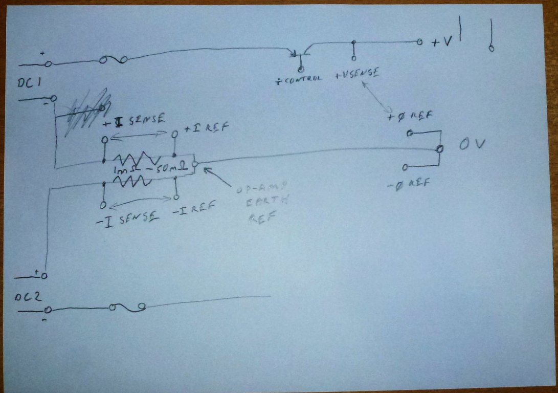
The higher current phantom earth I drew in another diagram would solve these problems because the sense and drive currents would flow to the opposite voltage rail and not go through the current sense resistor. It also allows a place outside the op-amps for a small amount of heat to be dissipated without causing thermal drift.

The HFE v Icc graph for the TIP102/7 is very non-linear so there isn't really other solutions for this transistor. 

Alternatively you could use a high gain (MOS)FET so that you don't have the hassle of a second (phantom) earth. 

So, in conclusion, the problems you are having with current regulation are related to the non-linearity of the HFE v Icc curve of the darlington transistor in conjunction with the base drive current sink path. 

I just had a look in my parts box and found some IRFZ44N MOSFETs. A quick look at the spec sheets shows drive currents are in the uA range. Unfortunately it needs too high a drive voltage. There must be newer 'transistors' available like a MOSFET that would solve most of the problems. I am not up to date with modern transistors as I have been away from electronics for over 20 years. I do however know that the TIP102 is very very old lol.

  Are you sure? yes | no

The Big One wrote 04/02/2015 at 21:19 point

Thanks!

.

However I don't know that the problem you are solving here is the same as the problems that I am having. :-)  My theoretical knowledge is insufficient to know for sure, though... I am a software hack dabbling in hardware, so have a lot to learn!

.

The log post I made talking about current limiting problems is not so much talking about a problem with the transistor used to cut off current, but rather an intrinsic problem with using a shunt resistor to measure current: at high currents, there is a high voltage drop.  In my previous design, I had the current measurement shunt *after* the LM317, so the voltage drop would be seen at the load.  (Say, if you have the regulator set to 5V, and were pulling 5A, you would only get 4.5V delivered to your load).  The current limiting itself is working fine: if I set the limit to 500mA, the transistor correctly cuts it off at this value.

.

In my newer design iteration (not yet posted, but hopefully I will have something to share this weekend) I put the current sense shunt resistor in between the current limiting transistor and the LM317 regulator.  By doing it this way, the current can be measured before the voltage is regulated, so the regulator will be able to get the full 5V no matter what the load is.

.

I have some more testing to do (tonight, hopefully), and will share my latest schematics after I have verified my plans.

.

Cheers

  Are you sure? yes | no

Hacker404 wrote 04/02/2015 at 09:56 point

Here is an alternate current sense setup that you may be interested in - 

I added more pics here - 

http://hackaday.io/project/5079/logs

Run out of time .. back later, message me if you want.

  Are you sure? yes | no

Hacker404 wrote 04/02/2015 at 10:00 point

PS: On ebay there are plenty of shunt resistors. Some of them are cr.p. Don't buy the ones with the wavy link. The cheaper version of them are called open air shunt resistors. 

  Are you sure? yes | no

Hacker404 wrote 04/02/2015 at 10:02 point

PPS: Correction -  open air current sense resistors

  Are you sure? yes | no

The Big One wrote 04/02/2015 at 14:40 point

Thanks for the info!  Looking over it now.

Cheers

  Are you sure? yes | no

Hacker404 wrote 04/02/2015 at 08:15 point

I am downloading Kicad. 

Some things about shunt resistors. 

If you open up a $5 multimeter that has a 20A range you will find that the shunt resistor is actually a bent piece of thick wire, like fencing wire but a bit thinner.

You can buy 5 Watt wire wound resistors down to about 0.1 ohms. You can stick lots of them in parallel for lower resistances but you need lost of copper surface area on the PCB or the solder joints will have more resistance than the shunt. 

You can buy specialised shunt resistors and that is probably your best bet. For prototyping you can file a slot in a nail until it has the right resistance. 

You need separate traces for the two sense points that are not a part of the current path.

With an op amp you can have very low value shunts but this has other issues. 

Higher shunts have higher voltage drop which is a good signal to electrical noise ratio. The disadvantage being the voltage drop itself.

Lower value shunts can me amped with an op-amp but the op-amp needs to be more sensitive which means it is also more sensitive to noise so the PCB has to be laid out right so the sense circuit isn't too long or too far away from the sense point. I don't have specific measurements for this so it's a case of give it a go and see. 

Current / Voltage limiting. I wish I could draw circuits lol. Perhaps I can hand draw then if you are interested. 

The same transistor can do both voltage and current limiting. Have a low resistance output on the current limiting op-amp and then a diode. Have a higher resistance output on the voltage op-amp. Diode is off when current is below set point. Above set point, diode is on and current op-amp takes control as it has a lower output resistance.

I could draw some pics. The shunts can be in the centre rail and that would save some issues. A phantom earth could fix the slight problems it creates if there are even any to fix. With low shunts you probably wouldn't need a phantom earth.

  Are you sure? yes | no

Hacker404 wrote 03/24/2015 at 01:45 point

Wow, Looks a thousand times better. Some things I would perhaps have done ...

First to explain why op-amps don't make good current drivers ...

Most often the output from an op-amp is a very small difference voltage while the source voltage (power rail) to the op-amp is much higher. This in effect cause the op-amp to dissipate the power (delta V * A) as heat. While the heat is small it is being dissipated right on the die of a chip that has a weak point with thermal drift. 

By increasing the gain of the driven stage the op-amp thermal drift can be substantially reduced.

This is exactly what you have done by using a darlington transistor as the driven stage. 

You could do the same with Vreg stage. Luckily the LM317T has a very sensitive input so this is not at all essential.

The current and voltage sense inputs to the microcontroller will have some offset, especially the voltage sense but you can fix this in software to save putting pots in the circuit board. 

The 1uF filter cap on I_GET seems a little high to me. At 1uF you will most likely use an electrolytic capacitor that has high series inductance and equivalent series resistance. I would have used a 0.1uF so that I could easily use a monolithic or tantalum cap that has lower inductance and ESR. 

You could also place a cap on the V_GET. Also one on the base of the darlington but a much lower value to absorb any transient spikes (only small) that come from the DAC. 

Over all, this is looking excellent.

  Are you sure? yes | no

The Big One wrote 03/24/2015 at 02:12 point

Thanks for the comments!

I am (right this minute, actually) working on a few more changes, related to your comments.

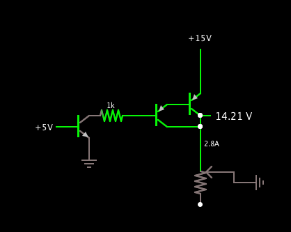
First, I am changing the driver of the darlington base from the op amp to being driven via a 1k resistor from VA.  The current limiting is done by using a small NPN to drain current from the base of the darlington.  The reason I am trying it this way is that in the previous iteration, the output voltage of the op amp was maxing out at about 13.5v (with a 15v supply); this caused the output of the darlington to max out at about 12v.  Another couple volts lost from the LM317, and the final output was no higher than about 10v.  By changing how the darlington is driven, I can get another couple volts out of the darlinton, which when combined with a 16.5 - 17v supply should give more more than 12v output (which is what I am shooting for).

In the process, I am also working on reducing noise in the current limited output stage.  When I first started with this approach, I had a lot of ripple noise / oscillations when current limiting kicked in.  I have greatly reduced that, and I am hopeful that I can completely eliminate it.

I will be posting an updated schematic in the next day or two, once I get this round of testing finished.

Thanks for all your help - your last comment especially really helped to point me in the right direction.

Cheers

  Are you sure? yes | no

Hacker404 wrote 03/24/2015 at 02:47 point

Hi again. The base emitter junction of a bipolar transistor is normally about 0.6V so in a darlington I would expect 1.2V because of the two junctions. That means in you current configuration called 'common collector' or 'impedance buffer', that the final emitter voltage will always be at leas 1.2V below the supplied voltage. ie If you drive the darlington as hard as you can by connecting the base to the collector then the emitter will still be 1.2V below the collector. 

The other issue is that if you series bias the darlingtone and control the base with another transistor on the open collector configuration the you may have stability problems due to the high resultant gain. I didn't look at the specs but darlingtons are up above 500 in gain then add another transistor of say 200 gain and you have a gain of about 100,000. This is too high and it could be set off by someone lighting a gas barbecue across the road lol.

If instead you use a PNP darlington and invert the output of the op-amp then you can get to full rail voltage by driving straight of the op-amp without a series bias resistor or extra transistor.

I will go look at the schematic again because I am now sure of where the op-amp power rails come from. If the op-amps can swing below 0V then you can easily combine voltage regulation and current limiting in on darlington. Though this may not actually be an advantage with PNP darlingtons because you loose the dissipation (heat sink) of the second transstor. 

  Are you sure? yes | no

The Big One wrote 03/24/2015 at 03:16 point

My first design had both voltage and current regulation in a single transistor... it worked (for some value of 'work'), but was very unstable when current limiting turned on.  I could probably do a bit better now that I am figuring out op amps a bit better, but even then I don't mind my current two-IC design... as you say, it speads the heat out a bit better, and I have the board space, so why not.

.

I am not familiar with what you are referring to, using a PNP.  Which pin on the darlington would you connect VA to?  I assume C is connected to VA, and E is connected to V_CURRENT?  Or is that backwards?  (I am a complete n00b with power stuff... this is my first project.  I can honestly say that I have learned more about power theory in the past month than I have learned in my entire life previous to this project!)  Getting the full voltage out would be very handy.  I am using two isolated switch mode supplies for a source, connected together to get V+ / V-.   They are nominally 15V, but can go up to just over 17.  With my current configuration, I have them set to 16V and can get just over 12V out of the 317, but if I can reduce the source voltage to 15V and still get over 12V output that would be even better (less heat).

.

You can see my current schematic below.  This includes my latest changes, most notably controlling the current limit with a small transistor.  With the 100uF cap on the darlington's base, it seems to be very stable - in normal mode it is rock solid, in full current limiting mode it is rock solid, and even in the 'transition zone' in between the two it is quite decent (I am seeing some ripple on the output, but it is no more than about 0.5v p-p).  Without the cap there, things start to oscillate very heavily when current limiting is turned on.  The other thing that helped stability greatly was to add negative feedback to op amp U3D (the one which compares I_LIM and I_SET).  Previously it was just a comparator; by adding the feedback I get a steep (but not completely vertical) line when current limiting turns on, which seems to help stabilize things a lot.  By reducing the 100k resistor I can get less noise, but a the absolute minimum current is higher.  With 100k, my minimum current output is about 30mA.

.

Some other responses to your comments above... 

-Yep, you are pretty much dead on with the 1.2V drop across the darlington.  (I think I measured mine at about 1.3).

-The op amp rails are +/- 16, so the output can swing negative (I need this for biasing the 317 to go right down to 0)

.

Thanks again!

  Are you sure? yes | no

The Big One wrote 03/24/2015 at 18:55 point

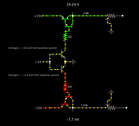
I think I have figured out what you are talking about with a PNP darlington.  Is this about what you meant?  See link below:

.

Circuit Simulator

.

Alternatively, here is a screenshot of the simulation:

.

By reducing the current on the base of the NPN control transistor, I can limit current through the PNP.

.

I'll give this a shot tonight.  Thanks for the suggestion!

.

Cheers

  Are you sure? yes | no

Hacker404 wrote 03/24/2015 at 21:15 point

Yes. This configuration allows you to get much closer to full rail voltage. You can actually get right to full rail voltage but do so you have to drive the darlington into 'saturation'. When saturated it can take some time to turn the darlington (even partially) off due to the effect of the capacitance between the base and emitter on the second internal transistor being amplified by the first internal transistor. This will give problems with response time when dealing with the current transients of a dynamic or complex load. To fix this problem place resistor between the base and emitter of the darlington to bleed off the the residual voltage from the base capacitance and design the darlington driver stage to accommodate the extra resistor. The base of the darlington wont get any lower than about 1.2V below the rail voltage (15V) ie 13.8V

The extra transistor is optional, if the extra resistor mentioned above is not too low in value then the darlington can be driven directly from an op-amp. If however you use the extra transistor then it would allow better decoupling for the op-amp power rails with one other change. What I am saying is that using the extra transistor means that the op-amp output will only need to be as high as 0.6V to drive the base of the transistor. In this case the op-amp could have a separate lower and decoupled power rails by using (for example) 7809 (LM317T09) regulators. The extra decoupling would provide stability against strong transient currents like when driving an inductive motor. The exception is the current sense input being so close to rail voltage. This also can be changed by having the current sense resistors in the 0V rail of the upper PSU and 15V rail of the lower PSU. If you connect these two rails *after* the current sense resistors then have a common ground reference. 

I really need to get some software to draw schematics. Can I ask what you use.

  Are you sure? yes | no

The Big One wrote 03/24/2015 at 21:46 point

I use KiCad (http://www.kicad-pcb.org/) for my schematics and PCB design.  Very nice and powerful, free / open source, actively developed (CERN has been funding a lot of recent developments), cross platform... the list of pros go on and on.  There is a bit of a learning curve, and a few quirks, but no more than for other packages (I have used Eagle in the past and find KiCad easier to use than Eagle, for instance).

.

The screenshot in my previous message is from the online circuit simulator at http://www.falstad.com/circuit/.  It is basic, but much easier to use than spice or similar.  Nice for throwing together quick examples / test cases.

.

As for the transistors, yep that makes sense.  I did a quick simulation and it looks like I can do the same thing for negative voltages using an NPN transistor.  (This is a requirement for me, as I want the same board to support both positive and negative regulation, depending on which components you use and which resistor bridges you populate).

.

The simulation showing the same thing for positive and negative voltages is attached here, with a screenshot below (still using a second small transistor to control the bases of the darlingtons, I will try driving directly with op amps later on).

.

I'll try wiring this up tonight and see how it works.  It is looking very promising, though!

.

Thanks again for everything!

.

  Are you sure? yes | no

The Big One wrote 03/24/2015 at 22:07 point

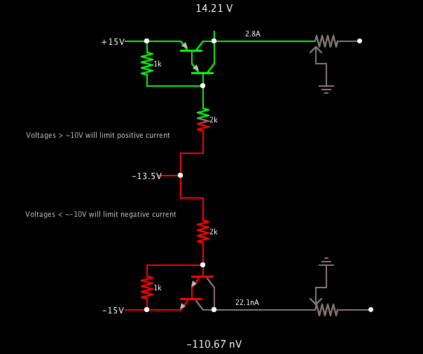
Here is another quick simulation showing what I understood from your description of direct driving the transistor with an op amp.  The +13.5V variable source represents the op amp here (my op amps can get to about 13.5V with a 15V supply, so this verifies that they are capable of shutting off the current).  Anything more than about 10V will limit positive current (less than -10V to limit negative current).

Of course, the real board will not have both positive and negative on it at the same time.  This is just in the simulator to ensure that the system works both ways.

.

When using a 2k resistor, the current does not exceed about 15mA, which is well within spec.

.

I like this approach better than reducing the rail voltage on the op amps for two reasons:
1) So far I have managed to avoid the need for an extra 7805 / whatever regulator on the PSU channels
2) I am using 2x quad channel op amps, and the other channels need higher voltage output; I would need to add another chip if I were to reduce the rail voltage on this op amp.

.

Cheers

  Are you sure? yes | no

The Big One wrote 03/24/2015 at 23:41 point

Yep, preliminary tests show that it works!  Using the PNP darlington driven directly from the op amp, I get about 0.95V more out of the current limited supply than I get out of the old version (15.35V from 16V rails, as compared to 14.6V from 16V rails).  As an extra benefit, I have a smaller BOM as well (no extra transistor)

.

More info to come as I do further testing.

.

Cheers

  Are you sure? yes | no

Hacker404 wrote 03/21/2015 at 09:16 point

Hi,

I see you're having a little trouble with op-amps. 

Here are some specs for this chip - 

Slew rate 0.6V/us

CMRR 70dB

Offset 8mV

Drift 10uV/C

The answer to the oscillation is simple - you are lacking shunt capacitors (signal to ground) and that is causing the oscillation due to the hi gain op-amp (G = 500 000) with a reasonable slew rate 0.6V/us

There is another  problem that I can see and I will try to explain it. 

The beauty of op-amps is that they work like an evaluation function to evaluate complex resistor / capacitor / inductor networks. Like an analog calculator. Really - you can throw the most complex network at it and it will get the right answer except for the following limitations. 

The bad points about op-amps is that they have a voltage offset and thermal drift and a tendency to oscillate because of their exceptionally high open loop gain (max gain). 

Your use of 'function blocks' is causing some trouble for you (instability). When you string function blocks (op-amps) together you are adding together a offset and drift for each stage. 

The rule for good op-amp design is to have one final stage (or one stage only) that compares the output with the reference input.

If I made an op-amp filter that had a low pass filter, high pass filter, rectifier, and a gain stage then I have four lots offset and four lots of drift in the circuit. I could however make all of these functions work with a complex capacitor resistor (and diode) network and only one op-amp and that way I only have one drift and one offset and a far reduced tendency to oscillate because I don't have lots of longer tracks on the circuit board acting like little antennas picking up signals from other stages. 

You can deal with the offset by using an external voltage reference. op-amps like the LM10 have this built in. The other alternative is a current mirror. 

Zenner diodes have an interesting property in that - zenners below about 5 volts tend to drift in one direction with temperature while zenners higher than about 5 volts tend to drift in the other direction. This makes zenners of about 5.6 volts very very stable with temperature so they make excellent voltage references.

More here -

http://en.wikipedia.org/wiki/Zener_diode

If you wanted a specific differential amplifier for the current sense then you could use the differential configuration commonly referred to as an instrumentation amp. Alternatively you could just use one op-amp for this. Then  a second for the voltage control. Both op-amp sensor could feed a common output. Just use a diode from the output of the current sense to pull the output reference low.

I would normally use a transistor for the output regulation because it has a higher HFE (Gain) and so needs lower drive current. op-amps don't make good current drivers.

  Are you sure? yes | no

The Big One wrote 03/21/2015 at 15:34 point

Wow, thanks for the info!  I'll keep this in mind.  I have thought of some potential alternatives to my current limiting (the only section that I am currently having problems with), and will see if your suggestions can help there.

Cheers

  Are you sure? yes | no

Michael Vowles wrote 03/08/2015 at 00:59 point

This is a great project looking forward to seeing your progress!

  Are you sure? yes | no

The Big One wrote 03/09/2015 at 18:37 point

Thanks!  I am making tons of progress here, although I have been a bit lax in commenting it as lots of things are still up in the air.

As a very short update: voltage regulation is hard.  :-)  My plans as currently designed (using discrete op amps for regulation) work at low load, but once you start pulling more than an amp or so it starts to oscillate.

I am now looking at other options, including off-the-shelf regulators like the LM317 integrated in such a way that I still achieve all of my goals (down to 0V, adjustable voltage and max current setpoints, digitally controlled, etc).  I am still playing with a bunch of different options, which is why I have not yet posted any of the new designs, but things are looking good so far.  More info will be coming in the next few weeks.

Cheers

  Are you sure? yes | no

signal7 wrote 02/18/2015 at 17:15 point

I'm curious what transformer you're considering.  Though they do tend to add weight and bulk over the choice of a switch mode power supply, they do offer a degree of isolation and a potentially quieter output.  For the quoted cost and specs, I'd be interested in building one too.

  Are you sure? yes | no

The Big One wrote 02/18/2015 at 19:10 point

I was looking at a few different Hammond toroidal transformers from Mouser.  18V, varying amperage for varying prices from about $65 to about $95.

That said, I think that I have decided to use switch mode converters after all.  I am still discussing whether to use one per channel (i.e. isolated channels) or whether to use two shared for all channels as a split rail supply.  There is a lot more options using switch mode supplies, and the price can be far cheaper (for low number of channels / low amperage).  Even for higher current / more channels, the cost is no more than a similarly spec'd transformer.

As I mentioned in my last log post, Exot and I are completely revamping the design, taking into consideration the comments mentioned in the featured article.  The design goals are mostly unchanged, but the implementation is going to look completely different from what I had originally posted.

Cheers

  Are you sure? yes | no

AVR wrote 02/13/2015 at 19:37 point

lookign forward to how this goes and to building my own variant with a touchscreen controller :)

  Are you sure? yes | no

Michele Perla wrote 02/13/2015 at 09:20 point

Dude, this is a very nice project; I always wanted a nice bench supply and this looks awesome. 

Kudos

  Are you sure? yes | no

Trevor Johansen Aase wrote 02/12/2015 at 18:19 point

It is not recommended to use wall warts connected in any way to get dual rails. They have a tendency to share currents and its only a matter of time before things explode. I had it happen first hand. Shrad has good ideas, I got my 48V 7.3A switch mode supply for $35 while a similar transformer from Antek was $75. I would personally not use the xMega as the brain as its more costly/finicky than its worth, an STM32F103 at $4 is much more capable and a Segger EDU JTAG for $70 is rock solid.

  Are you sure? yes | no

The Big One wrote 02/12/2015 at 18:22 point

Cool, thanks for the info!  I'll look around for alternative power supplies.

  Are you sure? yes | no

Shrad wrote 02/12/2015 at 15:21 point

ideas for you:
use a mosfet transconductance amplifier (voltage
commanded current source, only needs an op-amp and a mosfet plus a
couple resistors) as your regulator (the same used for a laser diode
current source with voltage control) and control it with software P or
PI regulation for voltage or current
use a hall effect current sensor for 1/10 the cost of your instrumentation amplifiers
use
an industrial switch mode power supply to generate a DC bus for your
modules (like the VICOR flatpak 48V or 24V units, or even a 24V 50A
blade server PSU with built-in monitoring features you can have for $10
on ebay)


those three features could make the difference from $150 to $50 cost of base + one module

  Are you sure? yes | no

zakqwy wrote 01/30/2015 at 20:30 point

Great project. My ATX supply isn't great even when it works, and I'm having trouble justifying the investment in another lab-grade bench supply (I eBay'd an old Agilent unit). I'll definitely watch the progress on this one!

  Are you sure? yes | no

The Big One wrote 01/30/2015 at 21:29 point

Thanks for the comment! I'll be sure to keep things updated as progress happens.

(On a side note, I just received shipping notice for an XMega sample from Atmel that they have graciously provided... hopefully I will have receive it sometime next week, so that I can start some feasibility studies on the XMega MCU. I have lots of experience with the ATMega lineup, but have never even touched an XMega, so it will be like starting out all over again. I am hoping that the XMega's DAC will allow for very easily setting the voltage / current settings, and when combined with DMA may even allow for AC output. Here's to hoping!)


Cheers

  Are you sure? yes | no

zakqwy wrote 01/30/2015 at 21:32 point

Out of curiosity--why the XMega, rather than a simple 8-bit device? Better ADC resolution?

  Are you sure? yes | no

The Big One wrote 01/30/2015 at 21:44 point

The main reason I want to try the XMega is that it has a built in two channel DAC. While you can definitely use an external I2C DAC on a simpler device, doing that has a few downsides:

1) More board space + cost (the XMega that I am planning costs the same as a cheap I2C DAC, and is actually much cheaper than some of the more featureful DACs)

2) Slower / more CPU overhead if outputting waveforms (For some stupid reason I have it in my head that I would like to support A/C output). While you should be able to output a reasonably-well-defined sine wave at 60Hz when communicating with an I2C DAC, it would mean a whole lot of chatter on I2C. Add in the fact that other things are happening on the I2C bus as well (display updates, voltages / current readings on other channels, etc) and you could easily imagine that the waveform output jitters a bit. By using an XMega with DMA output to a DAC, you can continually output a waveform without any CPU intervention.

3) I want to play with XMegas, and this gives me the perfect excuse to do so ;-)

There are of course downsides to doing it this way as well. The biggest annoyance is probably going to be firmware updates: you would need to program each channel independently. I really don't like that idea, but I think that at least at this point the benefits outweigh the downsides, and once the firmware is completed, there won't be much need for updates.

  Are you sure? yes | no

Similar Projects

Does this project spark your interest?

Become a member to follow this project and never miss any updates