The Big One
-
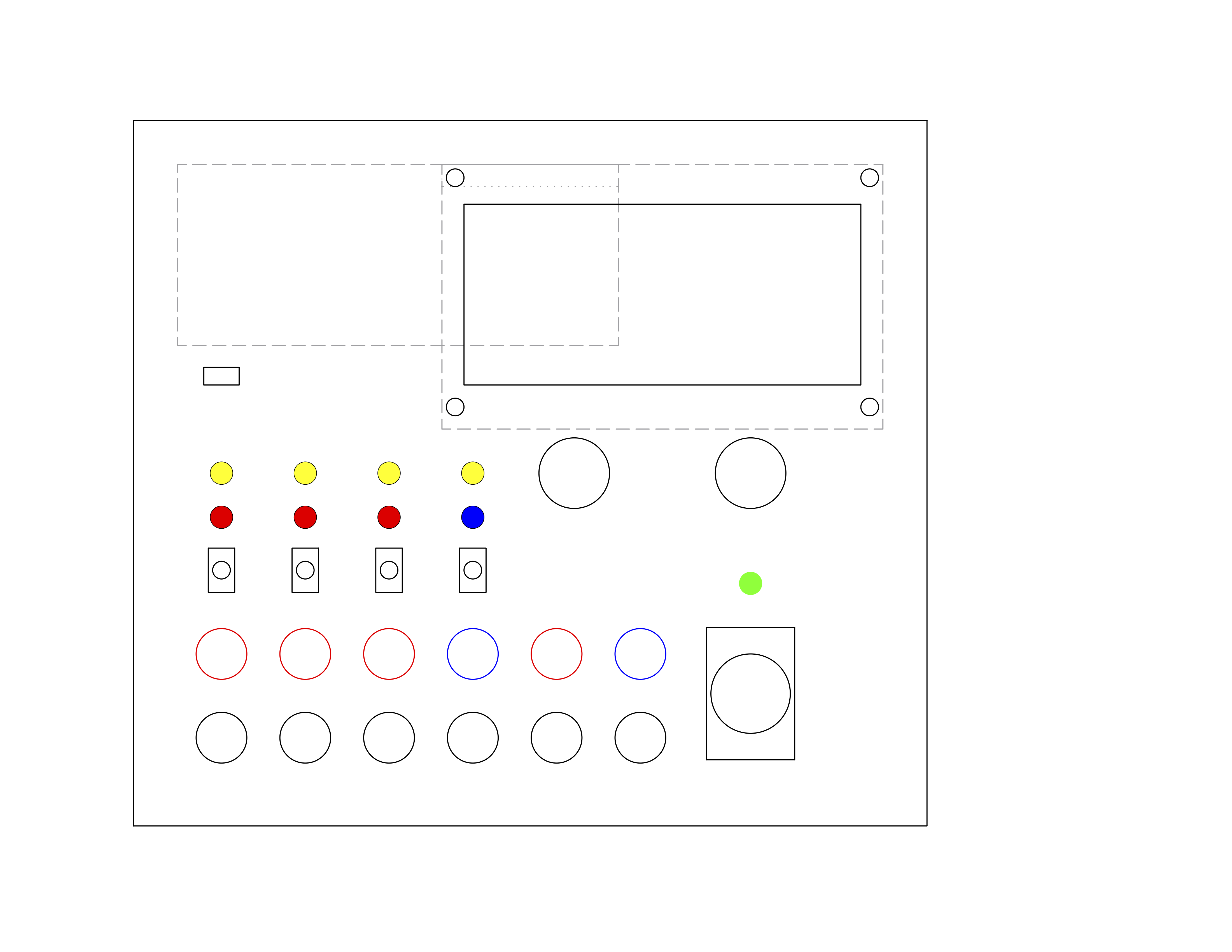
Front Faceplate (mostly) Finished
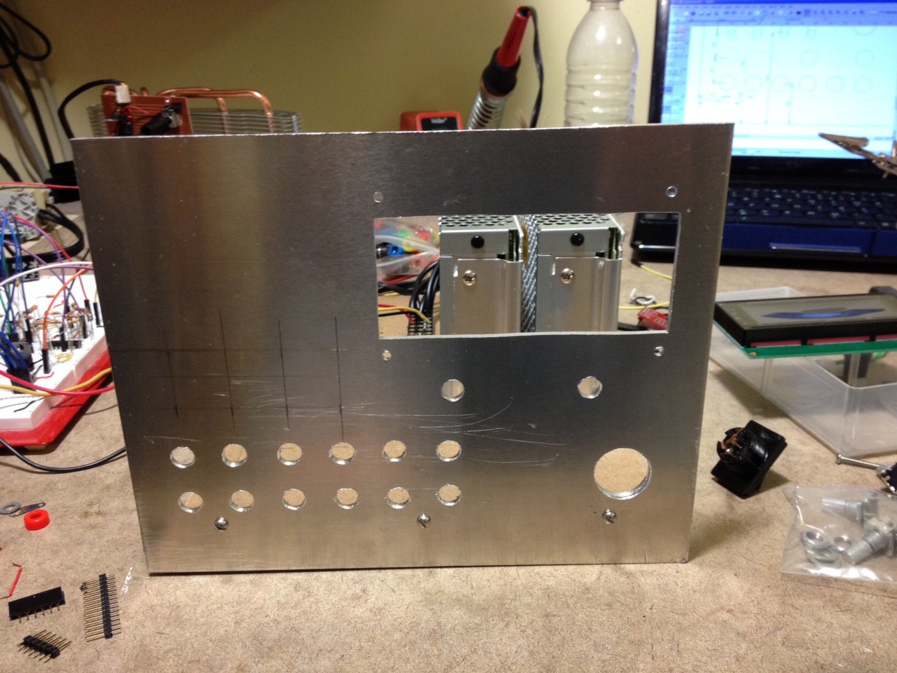
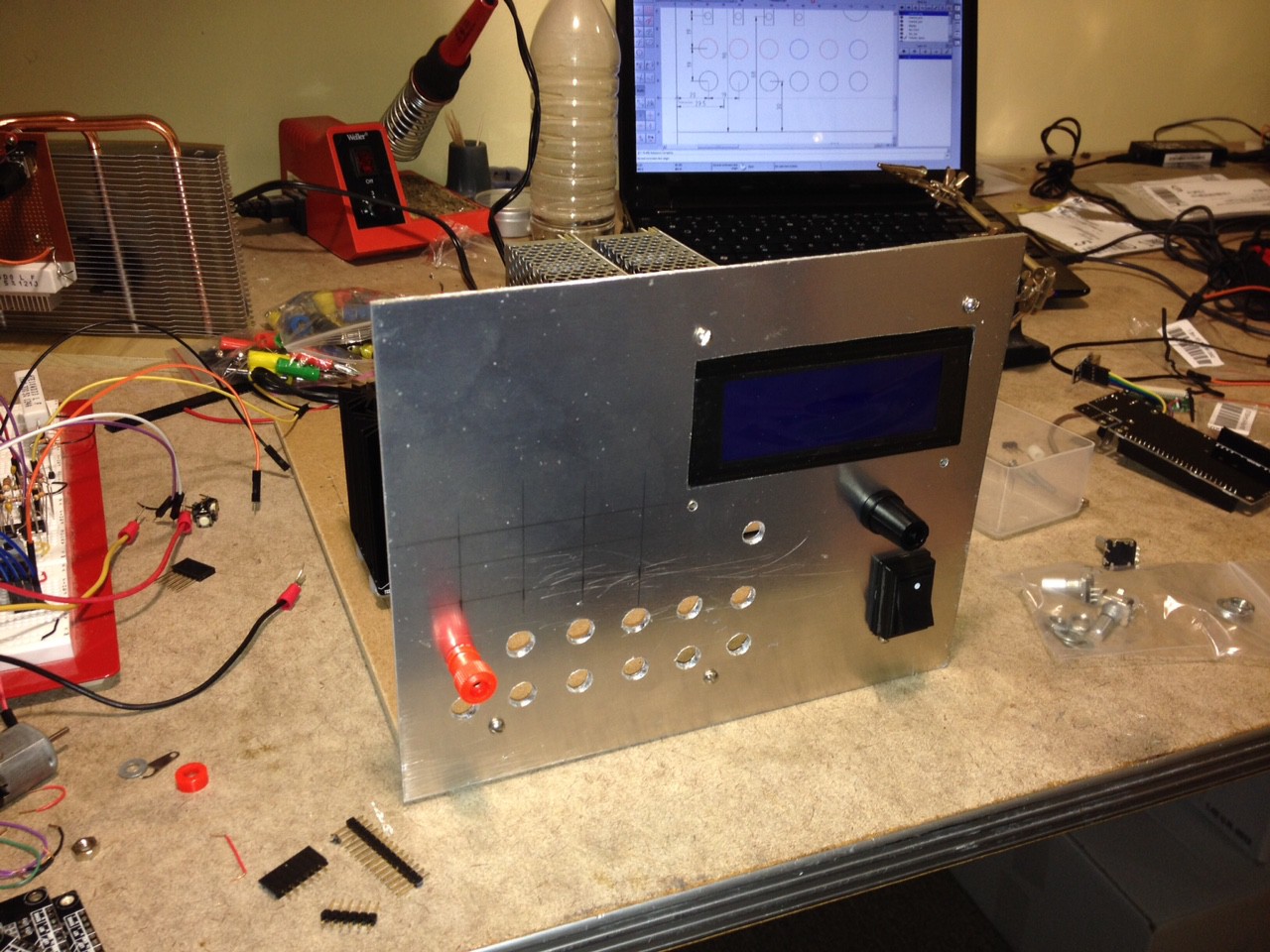
05/22/2015 at 17:53 • 5 commentsLast night I cut out the front faceplate. The hole for the display was cut on the scroll saw, the rest were done with a drill. I have 12 holes left to drill out, but I didn't have the right size of drill bits, so I held off until later (I am planning on hitting the hardware store today).
After all the holes are drilled I need to sand the front to give it the 'brushed' look.
Next step is to do the same for the rear faceplate (I need a large circular hole for a fan, a smaller circle for the fuse holder, and a non-circular hole for the power plug). Once that is done, I can get the first channel completely wired up and ready for use with the controller. Yay!
Below is a preview of what it looks like now, and with a couple of the components in place.
![]()
![]()
-
Footprint Update
05/21/2015 at 16:28 • 0 commentsI decided to change the footprint from 3/4" particle board to 1/4" hardboard. The reason for this switch is mostly convenience: I have 3/4" #4 screws, but I don't have 1 1/2" #4 screws.
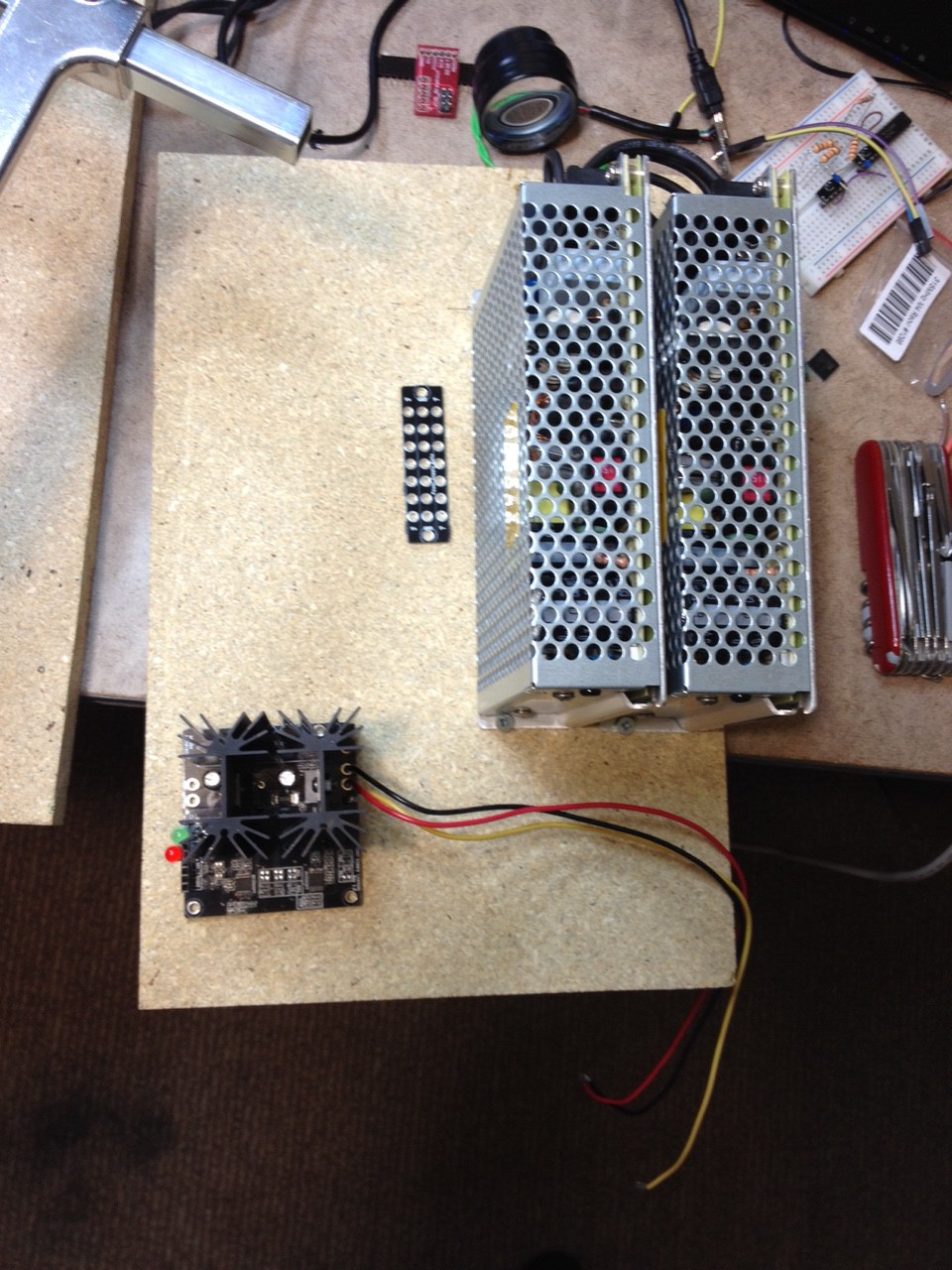
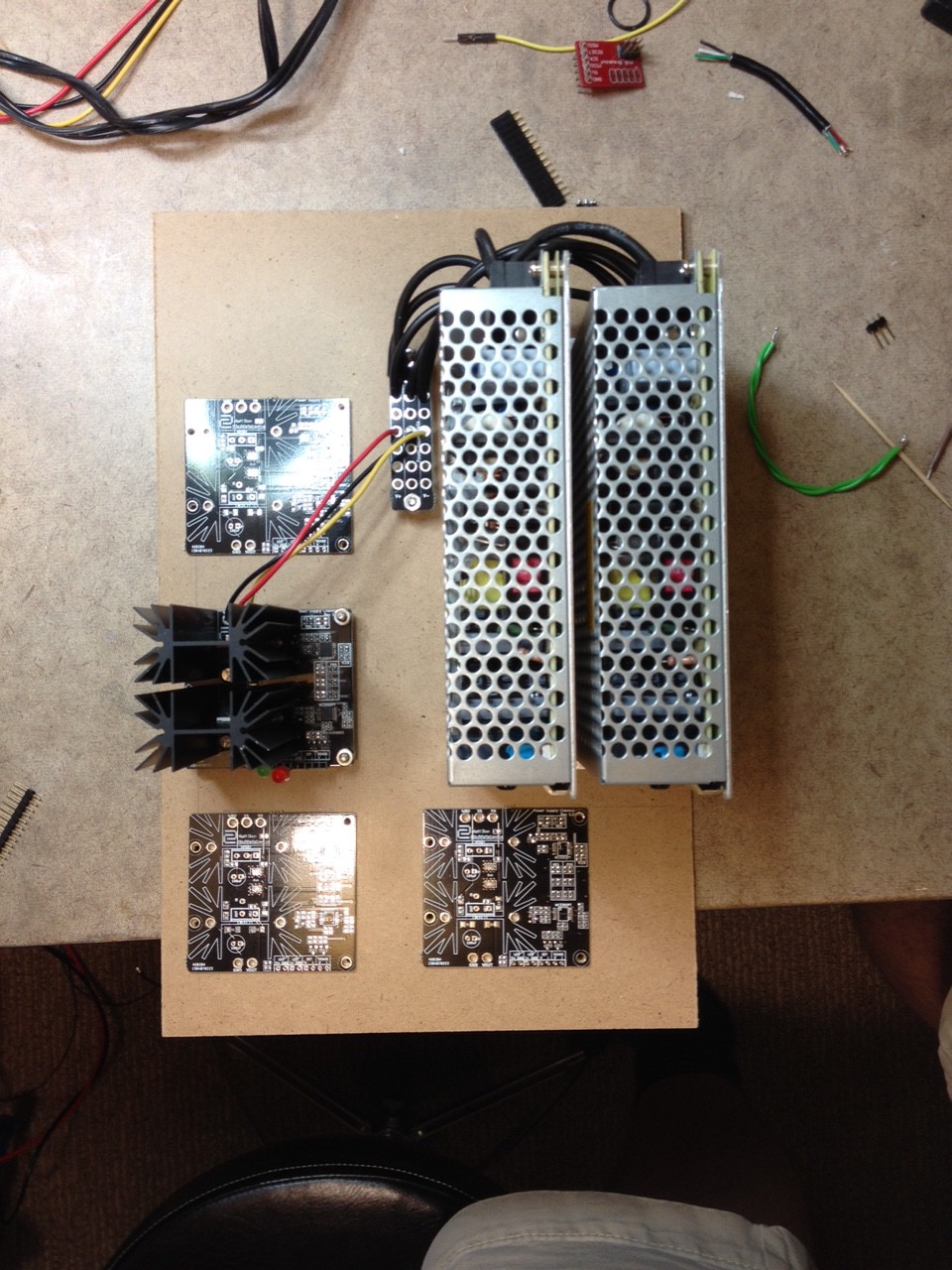
I have now also drilled the holes for all four channels' PCBs, mounted one channel, re-mounted the SMPSUs, and mounted the power rails. I had originally planned for the power rails to use screw terminals, but I think that directly soldering will give more resilience over time as well as make for a better electrical connection, at the expense of losing some flexibility.
Updated pictures are below.
Top view with approximate locations
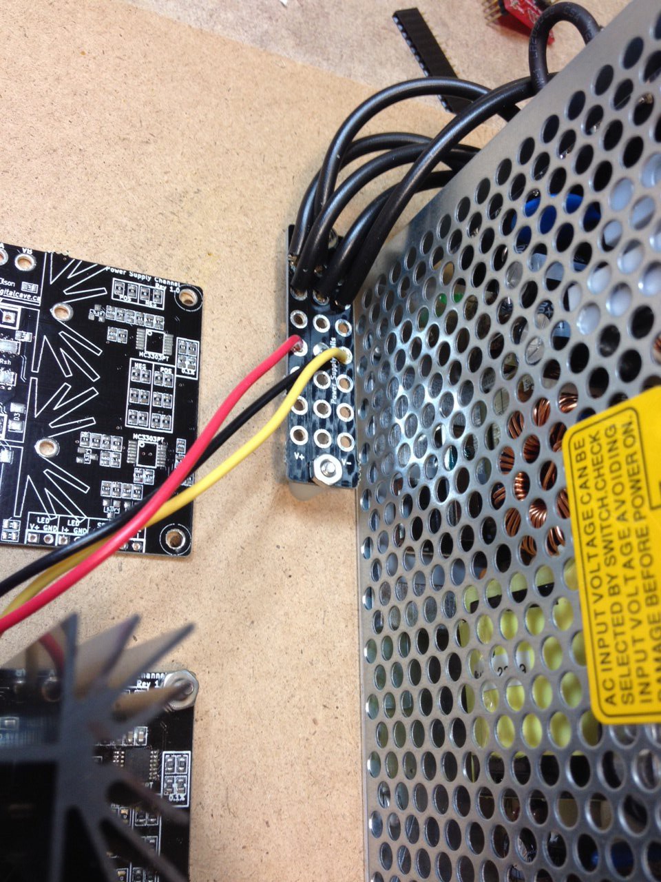
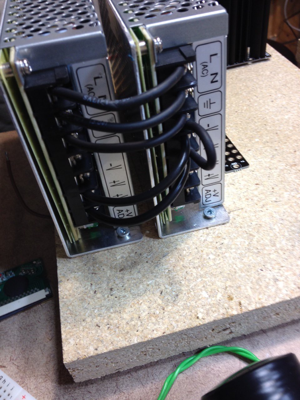
![]() Closeup of power rails. Two parallel wires connect to each connection in the SMPSU; one set of wires connects to each channel.
Closeup of power rails. Two parallel wires connect to each connection in the SMPSU; one set of wires connects to each channel.![]()
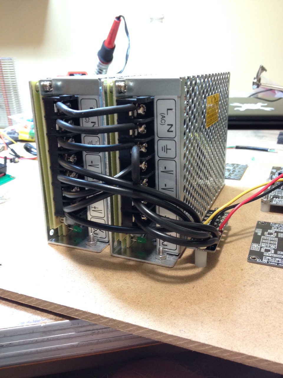
More wires
![]()
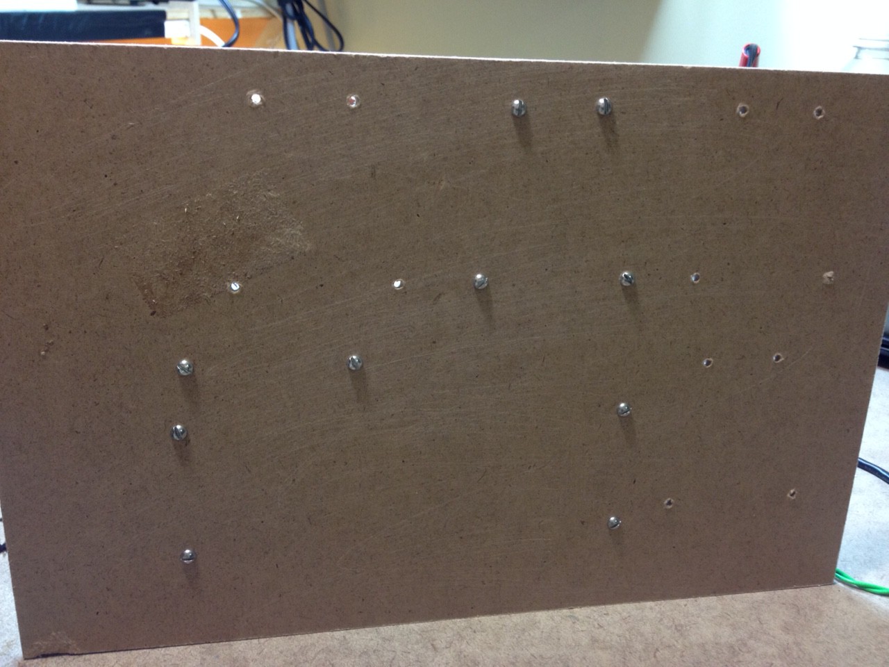
Bottom of the footprint. #4 screws are used to mount all the hardware; rubber feet will keep the screws off the table.
![]()
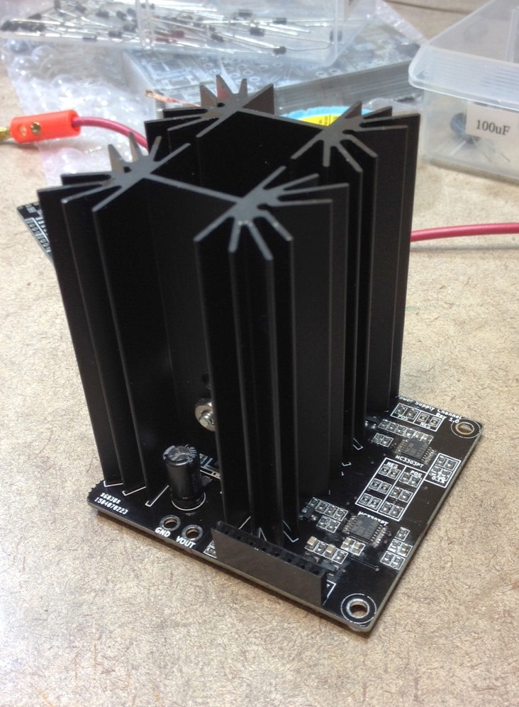
Closeup of a single channel mounted to the board. I still need to get some nylon nuts for the mounting holes right next to the heat sinks (I tried with metal nuts at first, and while it looks like they are not quite touching the heat sinks, and I have tested for continuity between the mounting holes and the heat sinks (there is no connection), I want to be sure that it does not short out later on. (The heat sinks are connected to live voltage: the transistor collector and the regulator VIN respectively, while the mounting holes are connected to ground).
![]()
-
Some Progress on the Enclosure
05/20/2015 at 17:27 • 0 commentsOn Monday I cut the aluminum plates for the front / back to size. I used a circular saw, which was terrifying (my brain was screaming 'why are you trying to cut metal with this!?!?'), but it worked out fine. Next step is to cut the holes (most will be done with a drill, but there are some sections which will require non-circular cutouts, which I will attempt to do with my scroll saw). I have done this before on a smaller piece, and it worked out fine... here's to hoping that these larger cuts will work too.
Yesterday I screwed the switch mode supplies into the footprint. I am using a scrap of particle board for the base of the enclosure, and all the components, including the front and rear aluminum plates, will attach directly to this. The cover will be of 1/4" hardwood, and will be mostly cosmetic (although it will help to channel the fan's airflow towards the appropriate components).
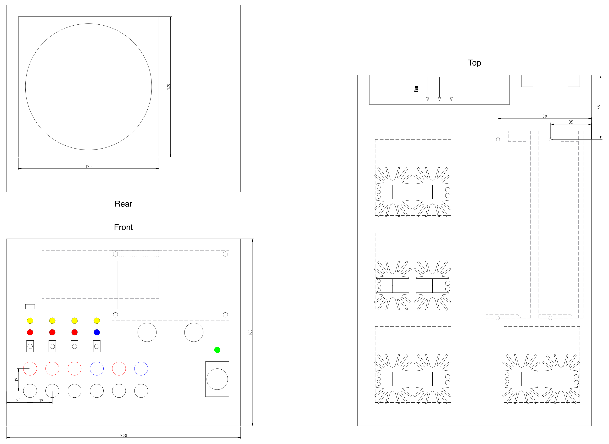
Here we have the current plan for the enclosure, as seen from the front / rear / top. (The rear is still lacking a bit of detail; it will have the AC code plug and a fuse).
![]()
Finally I have a couple pictures showing how the actual layout is progressing:
![]()
![]()
The next step is to cut the front faceplate, attach it to the base, and get one channel wired up, so that I can start doing some real testing on the channel + controller. (It is hard to test when high current wires are just hanging loose on the bench...)
Cheers
-
More ISP Investigation
05/15/2015 at 15:28 • 0 commentsWell, I did some more investigation into the ISP issues, and while I made some progress I still don't know exactly what is happening.
I ended up soldering a new controller board with just the AVR, crystal, and 8pF caps, and programmed the bootloader + fuses successfully. I then soldered the rest of the components, and tried ISP again, and it didn't work. Something in the circuit is interfering with the ISP programming.
The confusing part to me is two-fold:
- The circuit is very simple (the ISP pins are shared with the encoder headers, and the only components are a pullup resistor, a small capacitor, and a TVS diode; all programming testing was done with the encoders not installed).
- Obviously the capacitor / pullup could have something to do with this issue, so the first time I encountered it, I removed them: it still didn't work.
Now, to be fair, I had some clock issues the first time I saw this problem, so it may have been two issues coinciding that produced the confusing results. Regardless, I am a bit confused still. I will have to look into options for fixing this in future revisions (anything from a simple resistor to separate the ISP from the encoder, to perhaps a DIP switch to switch between the two).
-
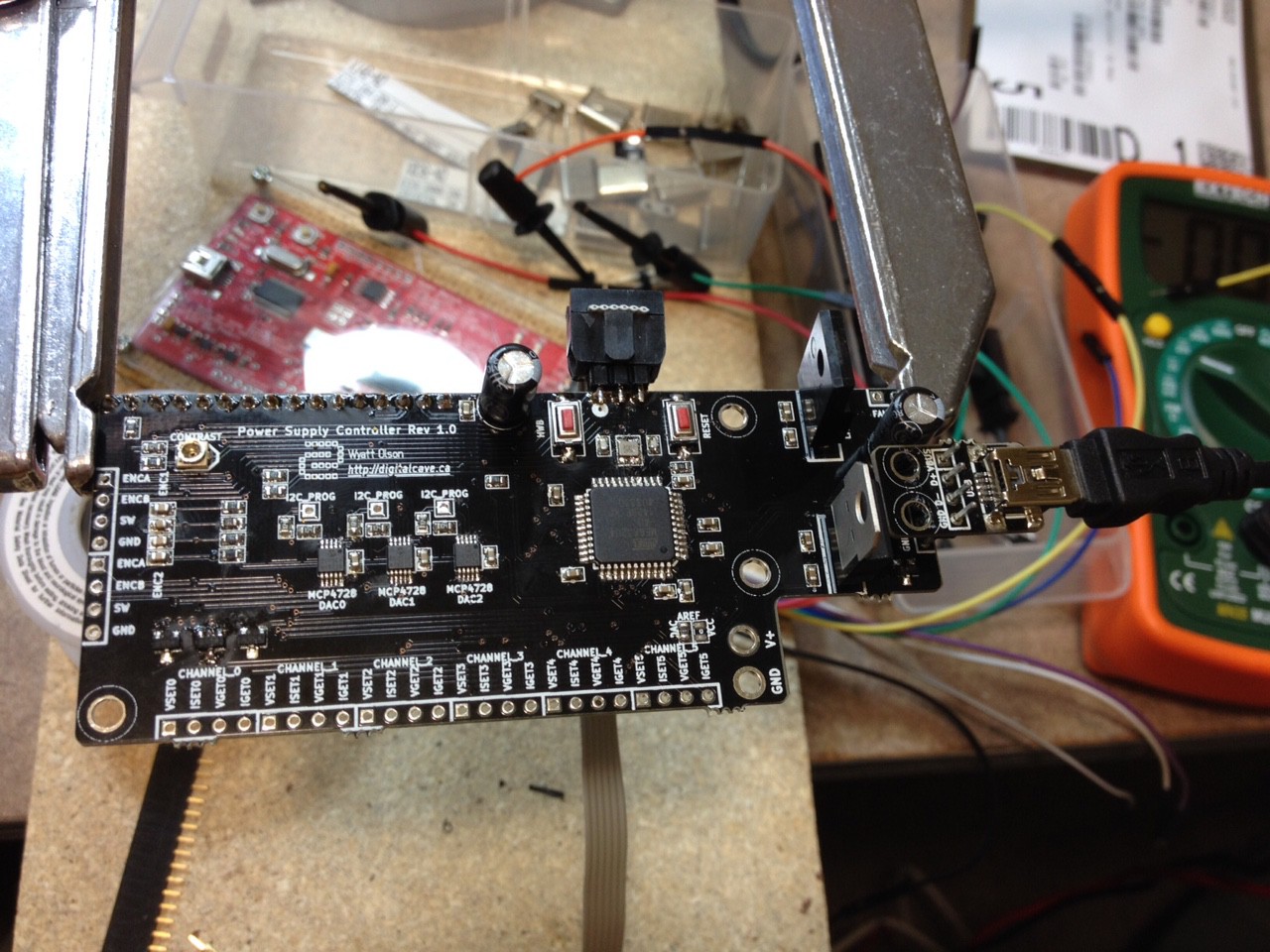
Working on Controller
05/13/2015 at 15:15 • 2 commentsI soldered up the main controller last night, but something is a bit off and I can't seem to program it using the ISP headers. The default bootloader works, though, so I am not quite sure what is wrong. More investigation needed.
I did discover one more error: the crystal footprint is rotated 90 degrees from what it should be. So, instead of placing it in 2.5x2 orientation, you should place it in 2x2.5. If that makes any sense at all. :-)
More updates to follow once I figure out what in the world is happening with ISP.
![]()
-
Boards Arrived!
05/06/2015 at 03:10 • 3 commentsMy boards arrived today, so when I got home from work I started to solder one channel up to see if things worked.
Spoiler alert: it works!
![]()
It took a couple of tries. Reflow soldering TSSOP chips is hard, and I still have not got the hang of it - there always seems to be one or two solder bridges hanging around, which are very hard to see even with a loupe. Also, I don't have the SMD schottkey diodes which I had planned on using, so I had to substitute a through hole diode with the leads trimmed to be a couple of mm in length.
So far I have found only one error on the board: the D3 diode is reversed. It shows the polarity pointing towards the bottom of the board, but it should be the other way. Sorry!
Below is a quick video showing off the beautiful soldered board in action... it was unrehearsed and done in one take, and hence rambles a bit, but hopefully it gives you an idea of how things look and work. Enjoy!
-
(Im)patiently waiting for PCBs to arrive...
04/24/2015 at 17:40 • 4 commentsOne month is a long time when you are waiting for boards to arrive!
As mentioned earlier, my PCBs are ordered and have been shipped a couple weeks ago. I estimate they will arrive in early May. Free shipping from China is slow, and I am too cheap to pay for faster shipping. :-(
![]()
The boards are shown again here... the board with the heat sinks will be used multiple times (once per channel, so I will be using 4 myself), while the other sections will be used only once (unless I can figure out some alternate use for them).
Furthermore, I am somewhat confident that the PSU channel board can also be used as a dummy load if you skip populating the regulator + headsink, and just short out the IN and OUT lines on the regulator chip. This needs to be verified still, though.
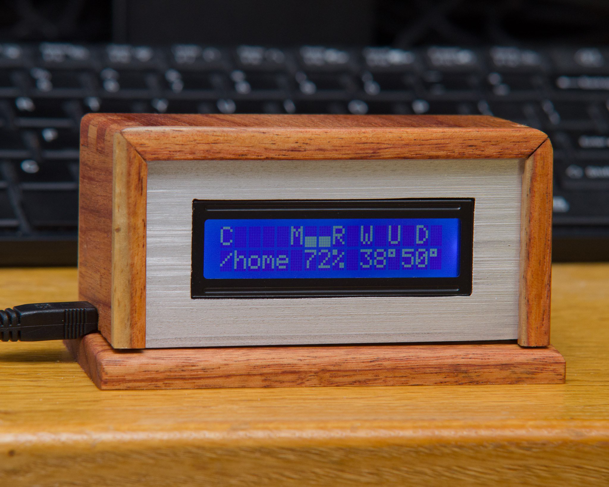
In the mean time I have been planning the enclosure. The faceplate will be brushed aluminum, and will look something like this:
![]()
The entire enclosure will be made of wood (with aluminum front and back plates), with an overall look similar to my resource monitor:
![]()
-
Boards Ordered
04/04/2015 at 17:37 • 0 commentsI submitted the board order today. If anyone is interested they can order their own (just keep in mind that I have not yet received my boards, and so cannot confirm that this rev 1 PCB works). The breadboard design does work, though, so here's to hoping that I have not made any stupid mistakes.
-
Gerber Files
04/03/2015 at 18:56 • 0 commentsA minor update to the previous log... I have generated the gerber files now, and everything is ready to go, pending no problems found over the next day or so.
You can find the zip file containing the gerbers on github.
Included in this gerber is the power supply (digital control, one channel for either positive or negative supply, and the power distribution rails), plus Rev 1.1 of the UBBB 32u4, and a small MSOP-10 / TSSOP-14 breakout. It all fits in a 10x10cm board, destined for manufacturing through Dirty PCBs.
Cheers
-
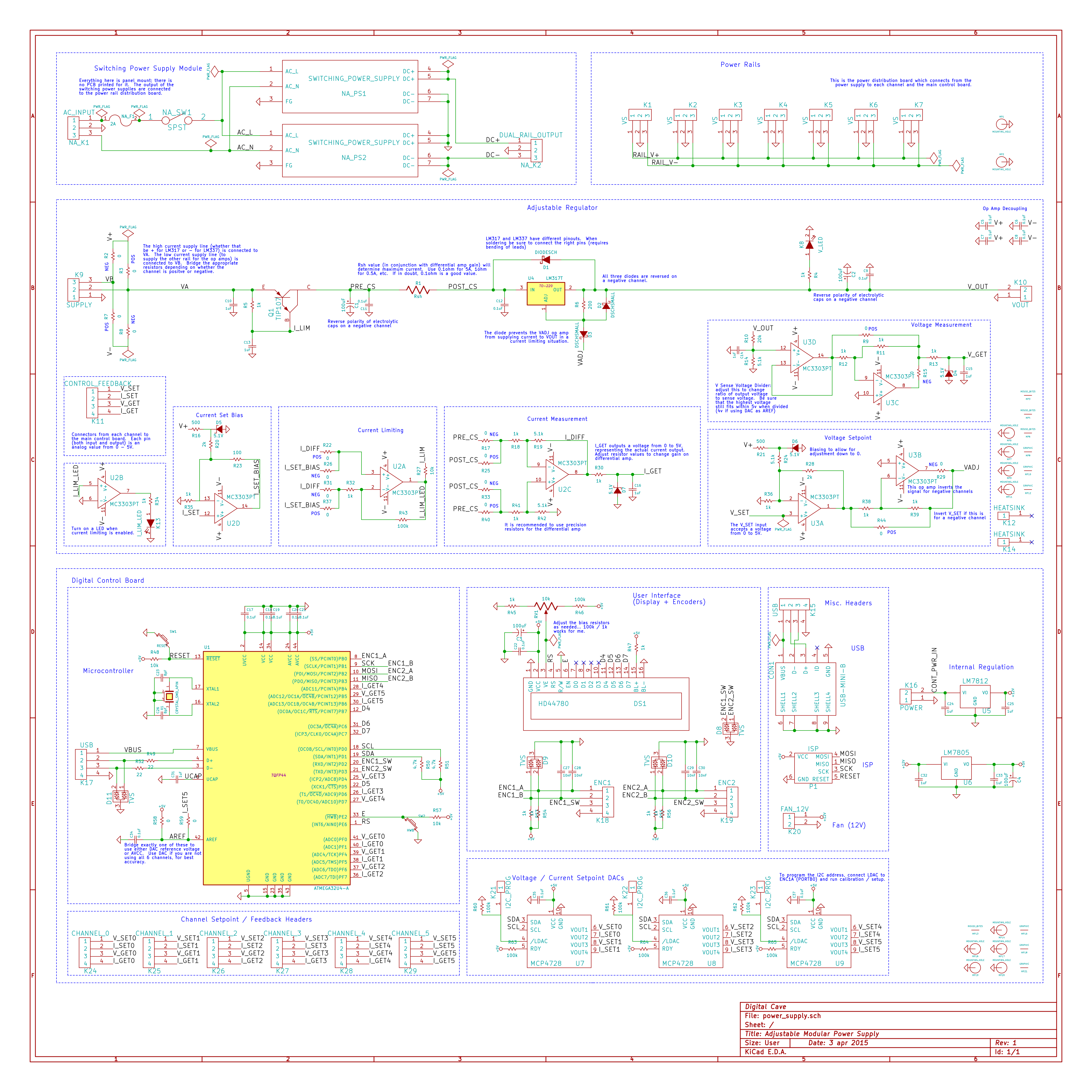
Final Design for Rev 1.0
04/03/2015 at 18:03 • 2 commentsI think that I have figured out everything that needs to be done here. Yay!
First, some comments on which of my original design goals I was successful with and which I was not.
The final design:
- Is modular, allowing for a variety of power sources (transformer + rectifier, dual switch mode supply, or even a wall wart (although the wall wart comes with limitations on functionality)
- Allows for up to 6 channels, with each channel able to be defined as either positive or negative.
- Each channel's voltage / current limit setpoints and voltage / actual current sense feedback is an analog value in the range 0-5V. They can be driven by potentiometers or DACs, and read by an ADC.
- Each channel to go all the way down (or up, for negative channels) to 0
- Allows a current limit setpoint all the way down to 0mA
- When using the digital control board, encoders + a display allow easy changing of set points and viewing of actual values
- The digital control board includes calibration and control over USB
- If you use less than 6 channels, you can assign the DAC output of channel 6 as AREF on the microcontroller, allowing for a more stable voltage reference which will improve the ADC accuracy
The biggest limitation that I was unable to overcome (without introducing extra complexity or other limitations) was when using a single supply (e.g. a wall wart); voltage regulation works (down to 1.25V instead of 0V), but current limiting seems iffy at best. Perhaps if a rail to rail op amp was used it would work better (I don't have any rail to rail op amps to test). That said, a split supply (whether it be from a scrap transformer or a couple of cheap isolated switch mode supplies) are cheap enough that I don't think running from a wall wart is really worthwhile.
Another limitation / bug that I can't figure out is the current limiting LED indicator light. It is supposed to come on whenever the actual current matches or exceeds the setpoint current. It works, but it tends to be delayed by a number of seconds (the exact length of time seeming to depend on the current limit setpoint: the higher the setpoint the slower it is). I am not sure why it does that... the actual current limiting kicks in immediately. It is only the indicator light that is delayed, and they are running from the same output.
The final schematic is below:
![]()
You will notice a few changes from last time:
- A diode D3 between the voltage adjustment pin and the voltage adjustment op amp prevents the op amp from sourcing any current to VOUT. It can essentially only 'pull down' the adjustment pin (if left unconnected, VOUT would rise to its maximum output of about 13.5V on a 16V rail).
- The current limit setpoint is now passed through an op amp U2D. This biases the output to go below zero, which is required for current limiting all the way to 0mA.
- I have reduced the value of some capacitors (most notably the capacitor on the I_LIM net, to turn the transistor on / off, and the size of the electrolytic capacitors on the main power line). The smaller values seem to be fine across all sorts of loads.
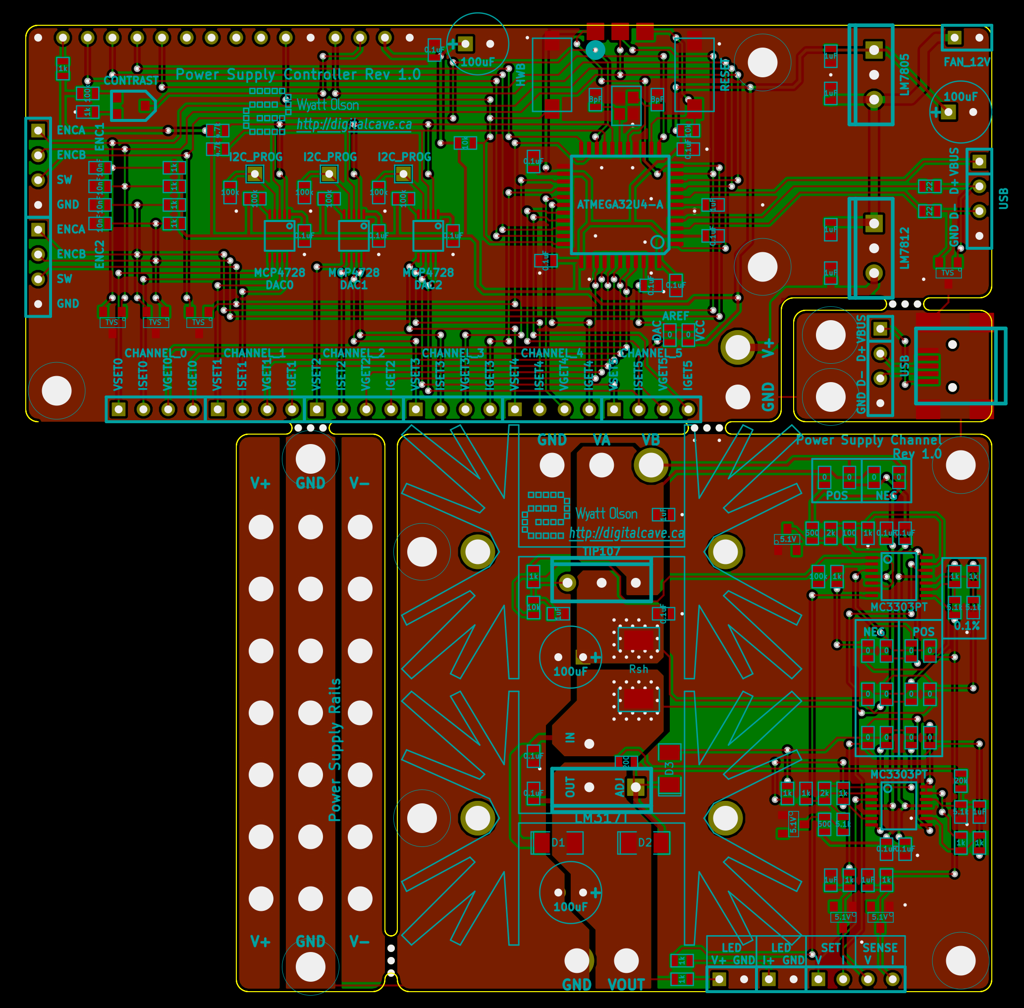
The board layout is also completed, and can be seen below:
I plan on waiting for a day or two to make sure that I have not forgotten anything, and then submitting the board to DirtyPCBs for manufacturing. If anyone in the community notices any issues, please let me know ASAP! :-)![]()
After the board has been submitted, I plan on working on the software some more. The basics are there and working, but there is still lots of room for improvement:
- The encoders could use some TLC; currently they sometimes skip signals.
- Calibration should use multiple measurements at common values (0, 1.8, 3.3, 5.0, 8.0, 12.0, etc) and interpolate in between them. This will allow for more accuracy across the entire range. This is especially important for current limiting, which does not seem to be quite as linear as the voltage setpoints.
- The user interface needs some improvement to allow quickly and easily setting voltage and current setpoints
- There should be some functionality for setting common values (say 5V at 500mA maximum to test a USB load)
- There needs to be more computer-side utilities for setting and logging data (all the USB HID commands are implemented on the AVR side, I just need to write a simple Python script to tie it all together).
I think that's all for now... feel free to comment below if you have any questions / comments / suggestions.
Cheers
Bench Power Supply
Designing an open source, modular bench power supply to rule them all.
 Closeup of power rails. Two parallel wires connect to each connection in the SMPSU; one set of wires connects to each channel.