-
Buck Converter Block
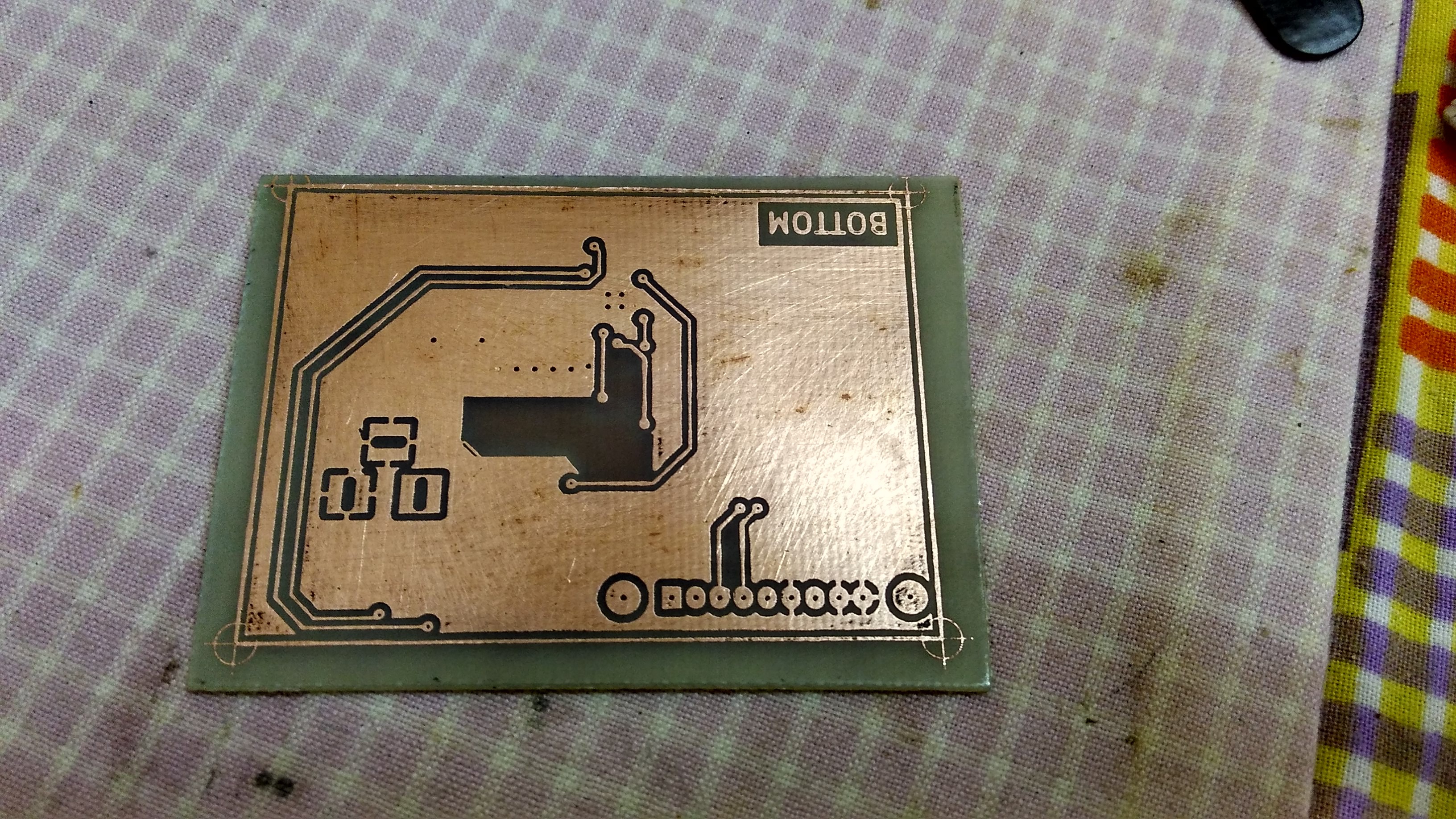
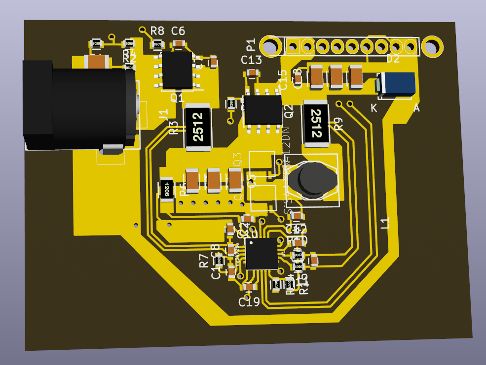
10/04/2015 at 17:15 • 0 commentsThis is the Buck converter block of the circuit I drew today. The LM3150 is a synchronous buck controller and by suitably choosing the MOSFETs and inductor I can easily get more than 10A out of it but for this application I need only 6.6A . Here's it configured for 5V operation.
![]()
The values were generated from TI's WEBENCH tool, and I made some part substitutions on the output capacitor (2x100uF tantalum + 10uF ceramic cap in lieu of OS-CON capacitors) and replacing the proposed MOSFETs with a power block.
You might be noticing that it seems there's only one MOSFET but it's actually a pair of n-MOSFETs arrayed in a H-bridge form - TI calls them power blocks and they seem to be optimized for power converters. It's an interesting concept, let's see how the converter performs when built.
-
Semifinalist Video
09/21/2015 at 18:30 • 0 commentsHere it is:I take a moment to wish all the other participants all the best with their Hackaday Prize entries!
-
New User Interface
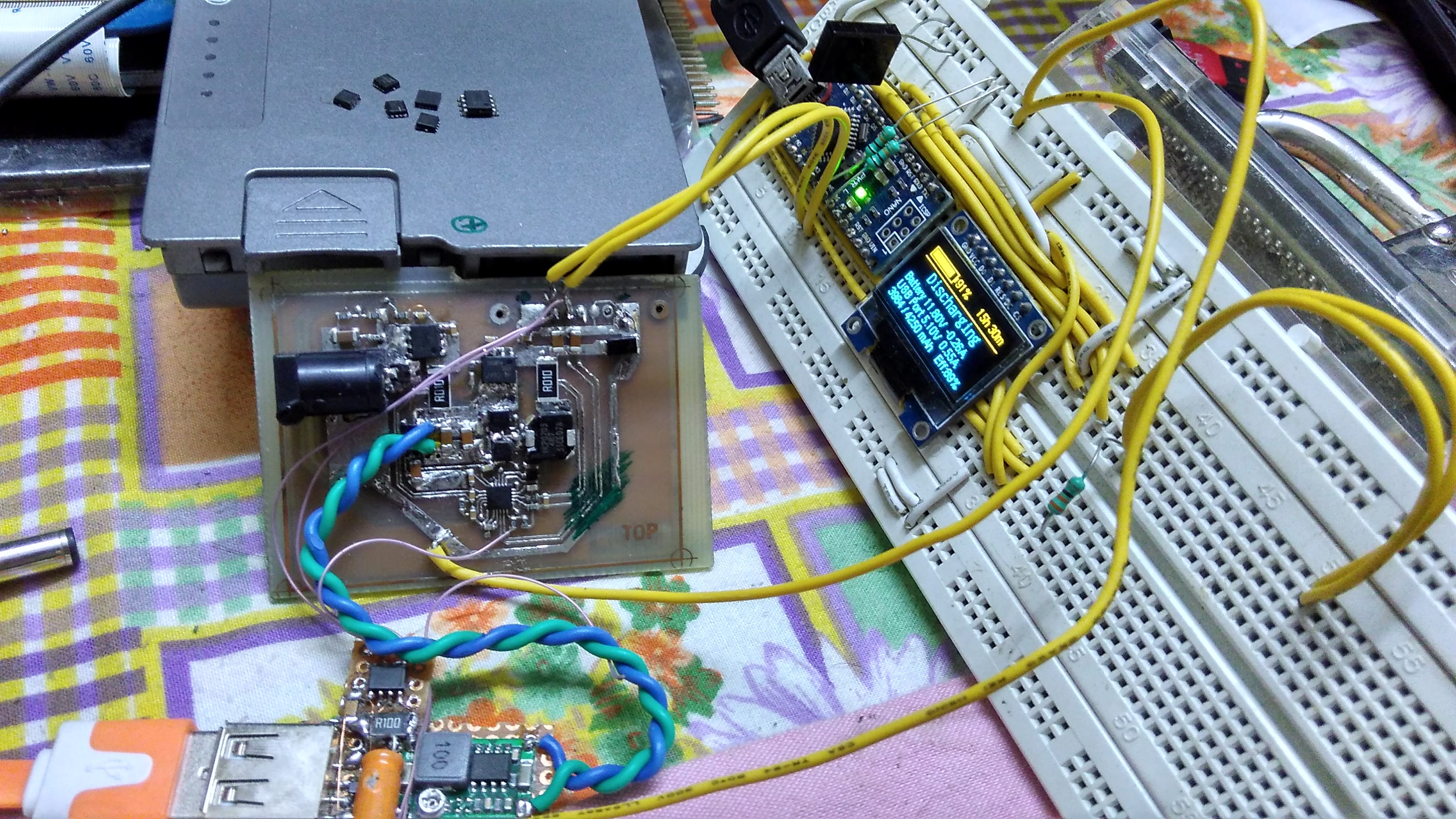
09/21/2015 at 18:25 • 0 commentsThis is the interface of the Power Pack which it uses to display status information,
![]()
This is currently implemented using an Arduino, I intend to use a STM32 ultimately. And it's just monitoring one channel for now. The battery icon is animated while charging which looks cool on the 2-color OLED Display :)
This is the code - github.com
-
Discharging
09/12/2015 at 21:42 • 0 commentsAlright, after charging I need to find a way to empty the battery so that I can recharge it again :P . After all this a smart power pack, not just a smart battery charger. Lo and behold -
![]()
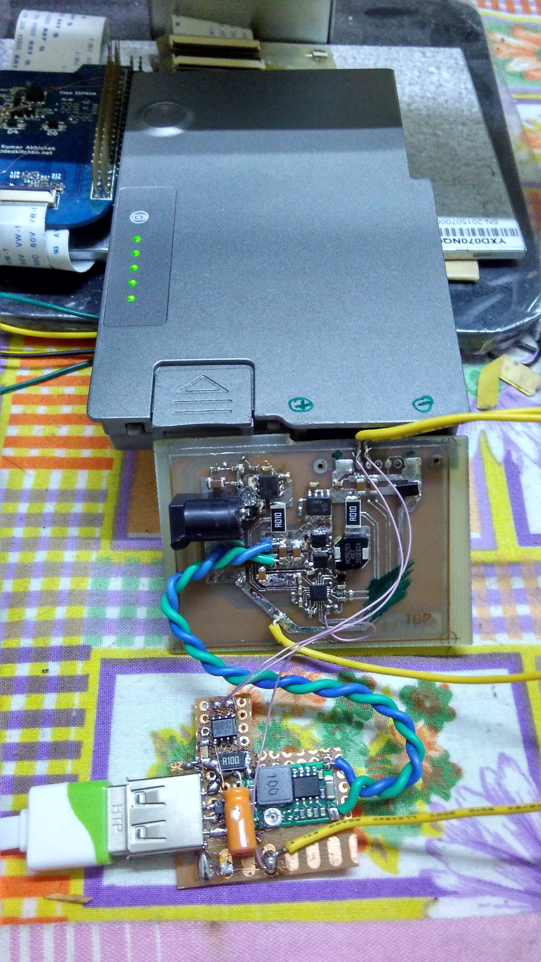
The bottom circuit consists of a 1$ eBay-bought buck converter - this uses a synchronous buck converter over the bigger LM2576 ones so they are much smaller. This is connected to the SYS voltage rail - the output of the adapter MOSFET. The bq24725a automatically switches on the other MOSFET to connect the battery to the SYS rail when the adapter is not present. When an adapter is connected, the adapter supplies power to the charger and the battery charges.
The 10uF electrolytic cap hides a TPS2513A which is responsible for applying appropriate voltages on D- and D+ pins so that the device being charged can draw maximum possible current from the supply (the converter should be able to able to provide 2A+ current.
There's an INA219A current monitor which uses a 0.1ohm shunt to monitor current flowing through the device. This can be used for efficiency calculations as well as you know V & I coming from the smart battery and V & I going out to the device - I see values around 86% efficiency which seems reasonable.
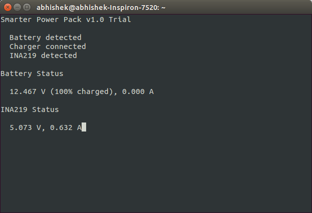
I also wrote a simple Python script (code here) using the curses library to provide an interactive display of the battery and INA219 values on the screen - here's a screenshot:
![]()
Zero current being drawn from the battery means that the buck converter is being powered from the mains rather than the battery! As soon as I disconnect adapter the battery will show a negative current flow indicating discharge. When charging, value of current is positive.
The final Smarter Power pack version will have 3 independent 5V outputs, and will be supervised by a microcontroller rather than my BeagleBone Black which I am using for prototyping right now.
Such a script would be great to have if the power pack is used to power the BeagleBone itself as a UPS - so the BeagleBone Black can take upon the role of a supervisor in that case. This script can run on the Pi as well and it can also be adapted to applications like automatically shutting down the system when battery is low, so on and so forth.
This is going to be really interesting now.
-
And... it's charging!
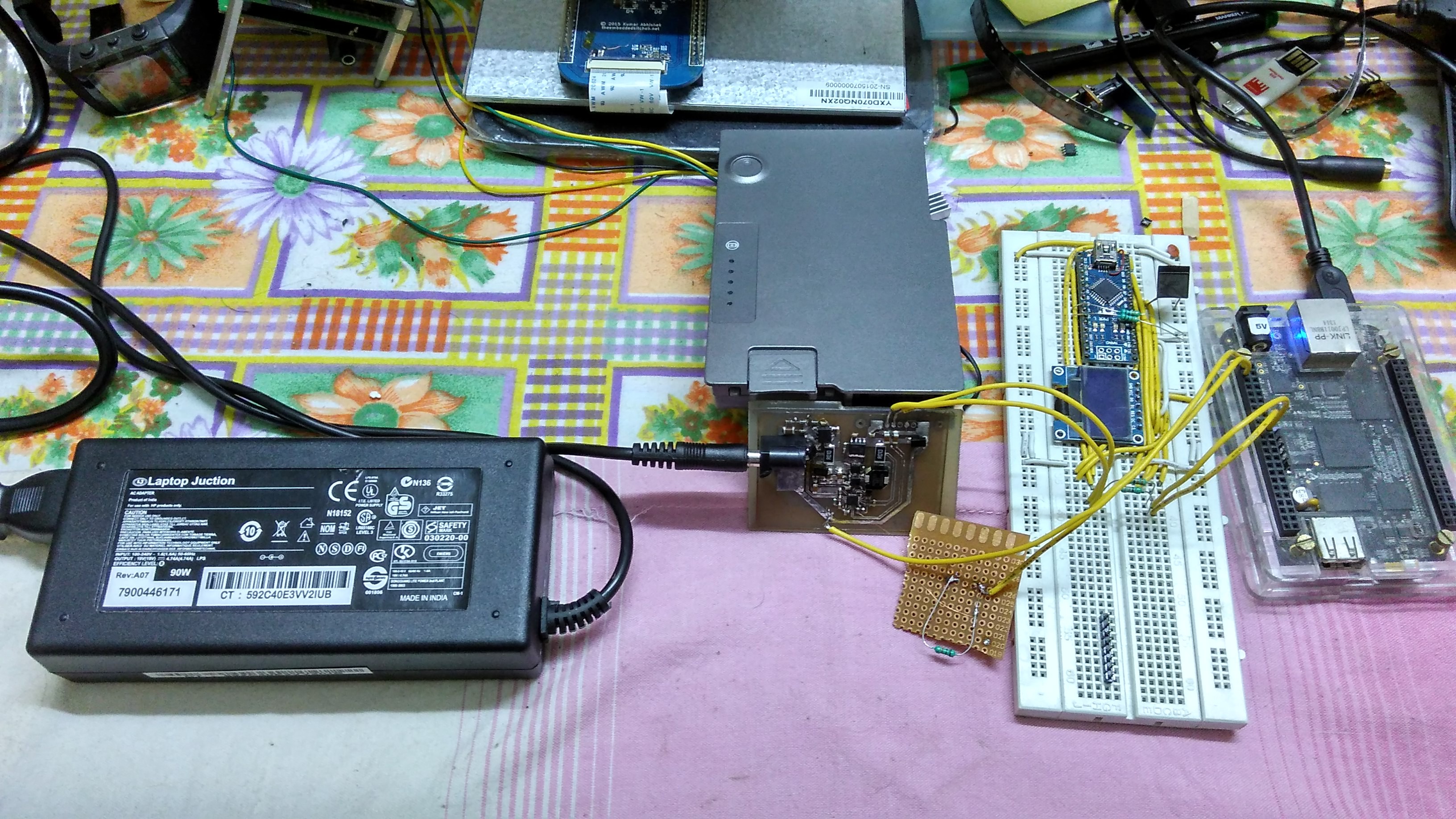
09/10/2015 at 15:11 • 0 comments6 shorted MOSFETs, an unusable bq24725a and lots of hot air rework later, I am so excited about the fact that the battery mentioned in the last project log is now being charged! This is my setup now:
![]()
I'm using my BeagleBone Black to currently talk to the Smart Charger and the Smart Battery using the "i2cget" and "i2cset" utilities. And I now have a shiny new Generic 19V (outputs 20V) 90W adapter for an ASUS laptop. If you're wondering, why ASUS then because I found it to be the only one which could well-fit in a standard DC barrel jack (there could be other brand chargers as well, let me know in the comments if you know any).
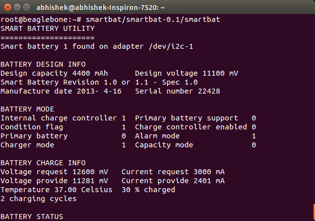
Here's a screenshot of the application running on my Desktop using which I am monitoring the process:
![]()
From completely flat to 30% in about half an hour is reasonable progress so far, and I'm so happy that this project is on track now. So now time for writing some firmware and completing the remaining hardware!
-
PCB Assembly
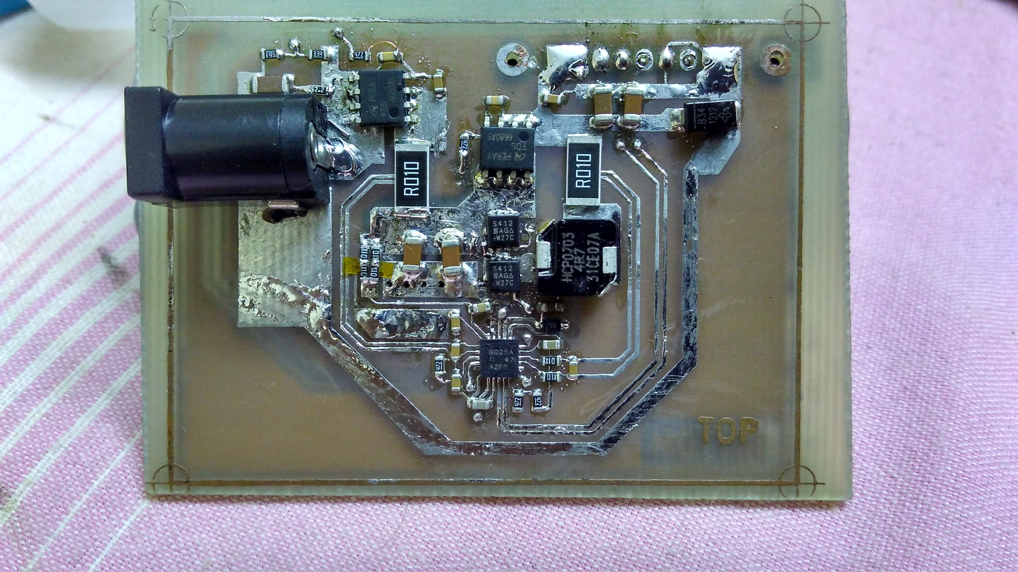
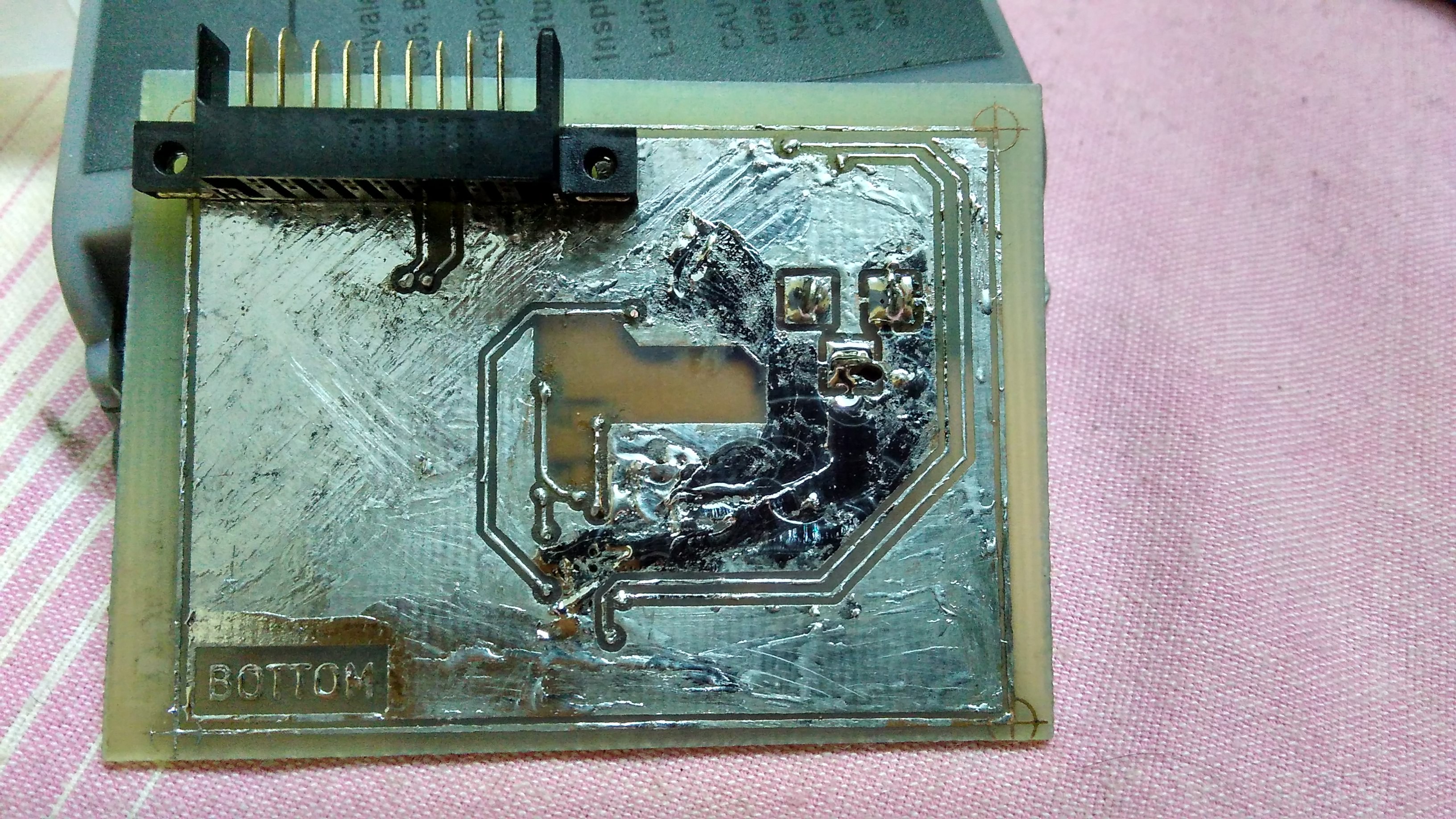
09/05/2015 at 20:47 • 1 commentI could sit gloating over my toner transfer results but I knew it wasn't going to help too much as I had to assemble my boards. So there were a few more steps:
(i) Manual "HSL" treatment - Coat the board with flux and then use the angled bit of my soldering iron to tin all the traces serving the dual purpose of protecting the copper from tarnishing and filling up any etch imperfections in the traces.
(ii) Drilling all the vias and connecting them - this is where the board fab wins hands down over home PCB fabrication. Also learning how difficult it is to use carbide bits and not break them. Used some single strand wire to fill the vias and cut them flush to the board surface after soldering. Then manually checking each and every connection with a multimeter to ensure they tunneled through the layer gap..
Okay, once all this is done, then apply solder paste on the pads and place every component manually. Then a quick reflow with a hot air gun.
Then solder the two through hole components - the barrel jack and the battery connector (on the other side)
![]()
![]()
Yes, it is very difficult to do solder-levelling on large filled copper areas.
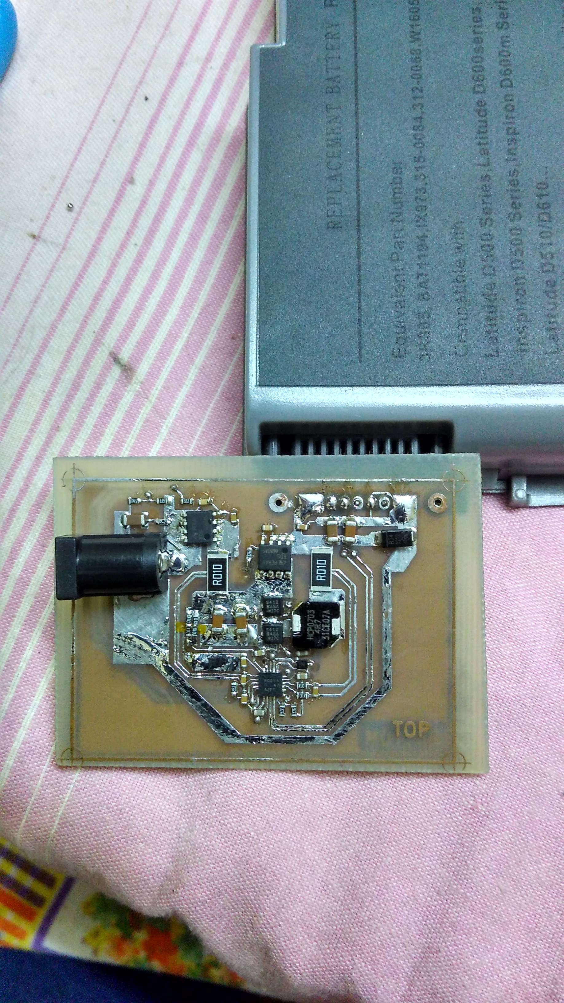
Attached on the battery:
![]()
-
PCB Fabrication
09/05/2015 at 20:30 • 0 commentsSince I was short on time, I decided to fab my own PCBs for this instead of sending it off which would have tied my hands for at least a week, so in two days I figured out how to use toner transfer to make my own PCBs. I was very apprehensive of the whole process but it turned out with better than expected results with a little bit of effort. Maybe it was the quality of the glossy photo paper that helped? I don't know. But I will document my toner transfer steps soon.
The first time I tried toner transfer, I etched my board with the FeCl3 "Sponge etch" method (use a sponge to rub FeCl3 all over the board). This worked against me as rubbing somehow reduced the quality of the etch and the traces came out when I took my solder iron to tin all the traces before soldering. I did another run the next day in which I just rocked the board a bit and left it in the solution. The boards turned out much better.
Here's how the etched boards looked after a bit of scrubbing:
![]()
![]()
-
Schematic and PCB Design
09/02/2015 at 20:53 • 0 commentsAll right, I spent some time drawing the schematics and ultimately realized that designing the full board, I won't apparently make it to the semi-final deadline with all the fabrication delays. So for the first part, I'm just designing a board with the bq24725a with the complete charging circuit and I'd be using a STM32Discovery board for doing the monitoring of this charger for now so that I can quickly prototype this. If the circuit makes it to the next round, it will probably be more polished and integrated into one set.
Here's how it looks in 3D render:
![]()
With this prototype I should be able to charge some laptop batteries. Once I am able to do that, I'll move on to the central controller.
And because I'm gonna fabricate this using toner transfer so messed around with GIMP to create A4 size tiled sheets of the artwork so that I can get 8 tries in a single paper print.
-
QuarterFinals Video Live
08/17/2015 at 17:41 • 0 commentsWatch it here.
I hope that the video gets the philosophy of the project across. Let me know if you have any suggestions/comments/feedback!
-
Choice of Microcontroller
08/05/2015 at 14:36 • 0 commentsA long idle period and I thought a lot over this and eventually decided to go for a STM32F103C8T6 microcontroller to control the system. I had initially thought of using an Arduino Nano but integrating a few libraries tends to fill up code space really fast, so there might not be enough room for expansion later. The IC itself is also available cheaply due to it being used in a lot of low cost dev boards from China, and I have a few spares lying so it'd be a good idea to engage them to work here.
I'm now beginning work over board layout of the charger section, although I'd seek some feedback on how many outputs you'd like to see from this power pack, after which I will complete the board and send it off to the fab.
Smart Battery, Smarter Power Pack
Fast Charging. Charge your portable devices. Use it as a UPS for your BeagleBone/Pi/Home WiFi Network. Or an emergency laptop power source.
 Kumar, Abhishek
