6502Nerd
-
dflat programming
05/30/2016 at 13:50 • 0 commentsI have decided to start a new log dedicated to dflat, the programming language I have built. I'll tidy up the other logs for duplication, but here will be detailed information and demos to show the capabilities.
I had an initial video of a demo space invaders type game on youtube but decided to replace it with something more extensive and some commentary which I hope helps. This is basically a complete game, takes up around 6500 bytes of source code (which is tokenised to around 4500 bytes in memory). It's extremely rudimentary, but about the quality of type in games found in magazines of the early 80s, so I'm not too embarrassed by the effort. During the programming of this game, I had some strange things occur which I traced back to a couple of serious bugs in dflat around the saving of state when calling a procedure - luckily not too difficult to fix.
I am still impressed with the speed of dflat. My old Oric-1 would have struggled..
-
Storyboard
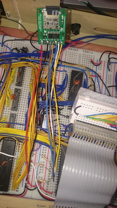
03/29/2016 at 23:27 • 2 commentsOk, so this part is not so much a blog, but a place to throw up the storyboard of my project through photos I have been taking from the beginning to present.
So I started very basic. I don't have pics of the 6502 in a free run set up, but the following images give a flavour of just how bare-bones it all started..
Clock and reset circuit, amongst the first thing I built and can be seen in the current set up. What's that tiny vero board on the right with a screw sticking out of it? Well it is my original power supply - stepping down from 9V to 5V. That screw is a heat sink!
![]() Initial decoding logic - don't even ask me what I was thinking! This has definitely not made it through to the current set up, in fact I never got to using it as realised it had impractical (or at the least worrying) levels of delay due to the number of cascading chips I was using.
Initial decoding logic - don't even ask me what I was thinking! This has definitely not made it through to the current set up, in fact I never got to using it as realised it had impractical (or at the least worrying) levels of delay due to the number of cascading chips I was using.![]() When I got hold of a TMS9918, I tried to work out if it was alive with a little free-run circuit. All it proves is that the TMS is getting power and a valid 10.738Mhz clock signal, so not really that useful with hindsight..
When I got hold of a TMS9918, I tried to work out if it was alive with a little free-run circuit. All it proves is that the TMS is getting power and a valid 10.738Mhz clock signal, so not really that useful with hindsight..![]()
This next pic looks like quite a jump, and in a sense it was - the main layout is taking shape. I decided to try and organise a central address and databus section around which I could wire up the necessary ICs. This board only has some ROM wired up but with an oscilloscope snooping the CPU address bus, I could verify that a programe was running and therefore, it lives! As can be seen, I am using a Winbond 27E512 (later on I stuck with a 27C512, but same wiring).
![]() Talking about oscilloscopes, I thought I shoud put up the core tools I used (and still do). First the oscilloscope. I had a 2Mhz bandwidth handheld puppy, but it was inadequate so invested in a USB connected one with dual channels. Without this I definitely would not have got the board running with all the components I have today.
Talking about oscilloscopes, I thought I shoud put up the core tools I used (and still do). First the oscilloscope. I had a 2Mhz bandwidth handheld puppy, but it was inadequate so invested in a USB connected one with dual channels. Without this I definitely would not have got the board running with all the components I have today.![]() Next, I have a EEPROM programmer. I did try to go down the authentic route and got myself some EPROMS, programmer and UV eraser! The edit/program/test/erase cycle was depressing so quickly moved on to the BATUPO - I tried some cheap far-East programmers (Top-Win anyone?) but this was and is way more reliable. This is now the most used tool of course as it's all about the software..
Next, I have a EEPROM programmer. I did try to go down the authentic route and got myself some EPROMS, programmer and UV eraser! The edit/program/test/erase cycle was depressing so quickly moved on to the BATUPO - I tried some cheap far-East programmers (Top-Win anyone?) but this was and is way more reliable. This is now the most used tool of course as it's all about the software..![]() The other thing I needed was a TV capture device. For a while this worked fine, but the delay on this is horrible, so now am using a regular LCD TV (as I have space in the office because we moved to a larger place in Summer 2015). Still, the TV Out was useful initially when office and desk space was at a premium.
The other thing I needed was a TV capture device. For a while this worked fine, but the delay on this is horrible, so now am using a regular LCD TV (as I have space in the office because we moved to a larger place in Summer 2015). Still, the TV Out was useful initially when office and desk space was at a premium.![]() I ran out of USB ports - Programme, Scope, TV Capture. And that didn't leave room for a serial port! So I needed a USB hub.
I ran out of USB ports - Programme, Scope, TV Capture. And that didn't leave room for a serial port! So I needed a USB hub.![]() My initial board was serial only using the 6526 (from a non-function CBM64) to bit-bang the serial line. I managed to get 9600bps reliably, before deciding to do things more properly and implement a 6551 ACIA. The board in this pic has ROM, RAM, 6502, 6526 all working well, with serial I/O the only means of communication. Even so, there is quite a lot of breadboard building up here, and it is starting to get awkward / delicate in moving it.
My initial board was serial only using the 6526 (from a non-function CBM64) to bit-bang the serial line. I managed to get 9600bps reliably, before deciding to do things more properly and implement a 6551 ACIA. The board in this pic has ROM, RAM, 6502, 6526 all working well, with serial I/O the only means of communication. Even so, there is quite a lot of breadboard building up here, and it is starting to get awkward / delicate in moving it.![]() I sent the following picture to my friend (sadly he passed away too young) when I was explaining the basics of what I had got going. The breadboards are now stuck to a plastic chopping board to keep them together! This is very much the current set up, but with sound added and the IO chips are actually 6522 VIAs rather than 6526 PIAs. The original clock and reset circuit is bottom left.
I sent the following picture to my friend (sadly he passed away too young) when I was explaining the basics of what I had got going. The breadboards are now stuck to a plastic chopping board to keep them together! This is very much the current set up, but with sound added and the IO chips are actually 6522 VIAs rather than 6526 PIAs. The original clock and reset circuit is bottom left.![]() More recent pics to follow..
More recent pics to follow.. -
dflat - a computer language
12/16/2015 at 19:12 • 3 commentsUpdate September 2016 :
I've added a token table which describes all the tokens that dflat understands - basically this is the list of statements, commands, functions and operators.
Core Features
The core features of dflat are:
- Integer only maths - just the 4 basic operators, plus comparison, shift and logical OR and AND
- Line numbers only used by the editor to store program lines in a sequence - no dflat commands directly refer to the line numbers.
- User defined procedures with parameters which can be made local. This is heavily inspired by the way BBC Basic did things.
- Simplified variable naming: Every variable has a prefixed type qualifier (e.g. %a is an integer variable). The opportunity with this is to perform easier syntax checking and runtime execution, which it does - sort of.
- Conditional and looping constructs : IF..THEN..ELSE..ENDIF, REPEAT..UNTIL, WHILE..WEND
- Array handling of scalar (integer variables) and strings. Integer variables can be 2 dimensional, strings can only have one dimension in addition to the length dimension that every string must have (this approach is inspired by Atari Basic)
- Execution can start at any procedure invoked from the command line - my own convention is to use "_start()"
Keywords
I thought perhaps I should just dump the keywords, functions and operators that dflat supports. Anyone with a memory of BBC, Atari or Oric BASIC will know most of these commands.
Current list of supported symbols:
- print, println : prints a sequence to output device, with or without new line
- def, enddef : define a procedure start and end
- dim : dimension one or more variables (up to 2 dimensions)
- repeat, until : repeat a section of code until a condition is true
- for x,y,z, next : initiate an iterative loop with starting value x, end value y and step size z. Works like a BASIC for loop but the variable cannot be specified in the next keyword
- if, else, elseif, endif : execute a section of code if a condition is true, else execute another section, else execution another section if another condition is true. Control passes to the next statement after endif.
- list : list the program
- load 'x', "file" : load a dflat program named "file" from device 'x', where x==0 means the serial port, and x==1 means the SD card
- save 'x', "file" : save a dflat program names "file" to device 'x', where x is as above
- input : take a stream of CR terminated characters and put in a destination variable (e.g. input $a)
- mode x : change screen to mode x, where x=0 means 40 column text mode and x=1 means 32 column colour mode
- plot x,y,c : at coordinates x,y plot character c. If c is an integer then plots the byte value, else if c is a string then plots the string from x,y
- cursor x : Hide the screen cursor (1) or unhide it (0)
- cls : clear the screen
- poke a,x, doke a,x : single or double byte write of value x to memory location a
- peek(a), deek(a) : single or double byte read from memory location a
- stick(x) : read joystick, and with mask x (to allow only a certain signal to be tested for). The joystick signals are active 0 as follows : bit 7 = fire, bit 6 = left, bit 5 = right, bit 4 = up, bit 3 = down.
- key(x) : read a key from the input stream synchronously (x=1) or asynchronously (x=0)
- setvdp reg, val: Set VDP register reg to value val (low control of the VDP is possible with this command)
- sprite sp, x, y, ch, col : set sprite number sp to position x,y using character pattern ch and colour col
- spritepos sp, x, y : set sprite number sp to position x,y
- sound ch,per,vol : set tone channel ch to period per and volume vol. If vol == 0 then channel will use envelope to modulate volume. If ch == 0 then set the period of the noise channel (vol is ignored)
- play te, ne, env, per: set up the tone and envelope configuration. te = 3 bit number for tone enable, ne = 3 bit number for noise mix with each tone channel, env = 4 bit envelope setting, per = 16 bit period.
- music ch, oct, note, vol: play music on channel ch, with note (0-11) and octave oct (0-6) and volume vol (0-15)
- left($a,%x), right($a,%x), mid($a,%x,%y),len($a) : standard string routines to get left, right, mid and length of a string
Some of you may recognise the sound commands - they are based on the approach used by Oric BASIC. This is both for nostalgia reasons and because both my computer and the Oric use the same sound chip.
I have a few unresolved bugs / limitations which I need to figure out and do something about:
- It's quite easy to crash dflat by mismatching variable types, so need more robust handling at the cost of a bit of speed
- String expressions are very limited. The best way to work on strings is to steadily build it up over a series of statements as it could go horribly wrong when trying to do it all at once!
- Numeric operator precedence is a bit bespoke! Every operator has a precedence e.g. + is higher than -, * is higher than /. So there is no such thing as operators with equal precedence. I will need to add a precedence table to fix this at some point - previously I thought I had made something that is logical but much simpler to implement, but I should have realised that Djikstra would have come up with this already if it was possible!
I now have the following features:
- Expression handler now does standard order of precedence. I thought I would need to use the shunting yard algorithm but when I started looking at it I realised it was much simpler (see below for more information).
- Basic data types of string and integer, with array capabilities for both.
- Flow of execution constructs: procedures, repeat..until loop, for..next loop, if-else-endif conditional execution.
- Input and output: input, print, println
- Basic graphics commands: mode, plot, cls
- Memory commands: Poke, Peek, Doke, Deek
Benchmarks
dflat has enough capability to try out benchmarks that test the performance of the language. I have used PCW (a UK monthly computer magazine) BASIC benchmarks from the early-mid 80s as this represents the closest era that my homebrew is equivalent to. The most complex benchmark tests the trig functions, but as my language is integer only (for now), the next most complex benchmark (number 7) is the one I have used.
I have tried to reproduce the original benchmark using dflat as faithfully as reasonable without trying to optimise further. Here is original and dflat code:
PCW Benchmark from early 1980s:
20 LET k=0
25 DIM m(5)
30 LET k=k+1
40 LET a=k/2*3+4-5
45 GOSUB 700
46 FOR l=1 TO 5
47 LET m(l)=a
48 NEXT l
50 IF k<1000 THEN GOTO 30
700 RETURN

dflat equivalent from 2016!
100 def_bm7()
110 println "Start"
200 %k=0
210 dim %m[5]
220 repeat
230  %k=%k+1
240  %a=((%k/2)*3)+4-5
245  _sub()
260  for %l=1,5,1
270   %m[%l]=%a
290  next
300 until %k==1000
305 println "Stop"
310 enddef
320 def_sub()
330 enddef
I got the benchmarks from the following site (* don't click on the nonsense adverts *):
http://www.geocities.ws/peterochocki/computers/pcwbm.html
Near the bottom of this page is a very interesting table of benchmarks for various old to new(ish) computers. I mentioned before that my expectation was that my restricted integer-only language should be quite a bit faster than most 1980s 6502 and Z80 based systems, save for the BBC Micro which is known to have a very speedy implementation.
I ran the benchmark a few times, and the result is....drum roll.... 7.5 seconds. I am very happy with this, it easily beats all the 6502 and Z80 machines of that era - including the BBC. Typical timings are ZX Spectrum 77.6s, Commodore 64 47.5, Atari 800XL 60.1s, ZX80 (integer only) 39.2s, BBC B 21.9s.
However, I need to acknowledge that aside from the simplicity (and therefore speed) of only working with integers, my system is also clocked at 2.68Mhz, which is significantly faster than all the other machines including the BBC. However, even adjusting for clock speed, dflat is significantly faster, and that is down to the major factor of unsigned integer arithmetic, plus extensive tokenisation and optimisation before and during runtime. For example:
- All variables are converted to look-ups as part of the syntax checking
- For and Repeat loop addressed are stored on the stack, so no inefficient line searching needed during iteration
- Once a procedure is invoked the first time, its address is cached so that further invocations are direct
I will now go on to some essential functions (save, load) followed by some useful graphics and sound functions.
The main challenge now is ROM space. Currently I have less than 1.5K remaining. This is starting to feel tight as I have a few more features to implement (e.g. more graphics and sound), but I haven't really space optimised the code so hopefully it will be enough. Plus I know that I can free up almost 1K of font data if I am desperate.
Introduction
This log is going to document my investigations and implementation of an interpreted language capable of running from ROM. Once doing this, my system will have the built in facility to write, debug and run programs without any external dependency - at the moment I have to use an assembler on the PC.
Initial Research
So, where to start in building a computer language? This has been done many times before of course, but the purpose of doing it for myself is the personal learning and hobby interest I have in knowing how stuff works. And of course the slightly egotistical pleasure of having made a language for my own requirements.
I have done a lot of background reading, relearning about lexers, parsers etc. I say relearning because this is taking back to my computer science undergraduate days - it's reassuring to find the concepts haven't changed dramatically.
The academic side of understanding how to design and build a programming language is good, but I have real world constraints - an 8 bit CPU with limited RAM and ROM!
I looked at Forth - a very compact language, fairly well suited for 6502. In fact I remember the 48k of the Oric-1 came with Forth on tape (alas, I had the 16k version). So if it can work on a 1Mhz 6502, I am sure it would be fine on my homebrew. But the reason for the compactness of Forth is the stack orientation, terseness and reverse polish notation which basically means that expression evaluation and parsing is made rather more straightforward.
So Forth is out, it doesn't feel like 'progress' enough for me! My first language was BASIC (I am of that age), so might be a natural choice. But I wanted to make an advance on 80s BASIC by having no line numbers - and therefore all program control is through structured constructs like procedures, functions and blocks.
The implication of no line numbers is that I would need a full-screen editor capability and this was going to take yet more ROM space (which elsewhere I have noted I am using up quite rapidly).
So I have decided that my language will use line numbers - but only as a way of inserting, editing and removing lines. The first execution statement will not be the lowest line number, but a 'main' type procedure. All flow of control will be through structured programming constructs - there will be no GOTO or GOSUB!
So I now need to develop the syntax. I'll post examples of the syntax as I progress - still thinking through the grammar.
Syntax
I spent a while trying to work out a syntax which was human readable but also easy for the machine to decode. Keeping it easy for a 6502 to decode will help me keep the code small and running fast.
Variables:
All variables must be pre-fixed with a type - one of $, %, ^ or ! e.g.
- %a : integer variable a
- ^a : byte / character variable a
- $a : string variable a
- !a : floating point variable a
I've decided not to support floating point right now - need to get something working first.
The program editor uses line numbers, but does not have control and flow keywords which refer to line numbers directly - the line numbers are purely to organise code in memory. Some examples below:
100 ; This is a comment
110 ; Next line is an example of a conditional.
115 ; ':' separates statements on same line
120 if %a > %b then:%a = %b:else:%b = %a:endif
130 ; _ is reserved to defined and invoke user functions
140 _myfunction(1, 2)
150 ; The next line defines a user function
160 def_myfunction(%a, %b)
162 ; make variables local scope explicitly else they are
163 ; globally accessible
165 local %a
170 return %a + %b
180 enddef
190 ; for, while and repeat all supported
200 repeat
210 %a = %a + 1
220 until %a > 10
230 while %a <> 0
240 %a = %a - 1
250 wend
275 ; for loop syntax simplified to specifying start, end, step
270 for %a = 1, 10, 1
280 println %a
290 next %a
295 ; strings have to be dimensioned before use, as do number arrays
300 dim $a[10], %a[10,10]
310 ; Note in the above that $a and %a are different variables
Will stop there for the moment - let me know what you think of the syntax. It has been inspired by various influences including:
- Atari 8 bit BASIC e.g. approach to strings and the pre-tokenisation of text
- BBC 8 bit BASIC e.g. user functions and local variables
- Oric-1 BASIC e.g. repeat..until loop (although other BASICs have this too)
- General BASICs e.g. for..next loops
Whether I get all the constructs working the way I want will depend on space.
Numeric expression tokenisation and runtime
This rather wordy subtitle is capturing some notes on progress. One of the more complex areas I have come across is expression parsing and execution. Let me give an abstract example of an expression using a simplified BNF type notation, restricted to numbers only:
<expr> = <term>[<op><term>]
<term> = digit[digit]
digit = 0..9
<op> = + | -
The above notation allows simple expressions like
- 1 + 2 - 3
Great, I can basically parse a syntax tree like this linearly. But what if a term needs to be more complex i.e.
<term> = digit[digit] | (<expr>)
So this allows me to make expressions like
- 1 + (2 - 3)
This is all still quite graspable I hope you will agree. Basically <expr> is recursive as it refers to itself (as part of the definition of <term>, and nicely implementable using a friendly language like C or Java, but how to do it nicely using a lowly 6502 with 3 registers!?!?
The main thing to worry about at assembly level is saving state when recursing, or trying to eliminate state altogether. Actually that's not possible - we have to know where we recursed from to be able to return to that point. But that part is looked after by the 6502 itself - making a subroutine call (JSR) automatically pushes the program counter on to the processor stack.
The interpreter takes a line of input and attempts to tokenise and syntax check before saving to program space (or executing if it is in immediate mode). I have an input pointer and output pointer which tell me where the next character to be processed from of the input is, and where the next tokenised character will go. I only advance these pointers when I am committed to taking them. Examples of where I may not be committed is checking the operator symbol table to match against multi-byte characters (the above simplified example misses operators like '<<' and '>>'.
So that means I can have an assembly routine called (say) tok_nexpr to tokenise a numeric expression. I only advance the input pointer when I am committed to consuming it, and when I see the '(', I call tok_nexpr again. On return I do a mandatory check for ')' as part of the syntax check.
So that looks pretty straightforward, once I had built all the scaffolding routines to deal with non-bracketed expressions, it was easy to extend to arbitrarily complex expressions to be tokenised.
But the runtime is more complex. Now we're not simply checking the input stream, but executing the tokenised output stream. An expression like 1 + (2 - 3) requires executing in the correct order - i.e. the brackets have to be evaluated before the rest of the expression.
I do this by maintaining an argument and operator stack when executing the numeric evaluation routine called (say) rt_neval. As the runtime is executing, any 'terms' it sees are pushed on the argument stack and any 'operators' are pushed on to the operator stack. When the routine first runs, it pushes a 'floor' value on the operator stack so it knows how much of this stack was used during this evaluation. When the routine has pushed all arguments and operators, it is ready to process. It does this simply by popping an operator, and then invoking the operator code (e.g. the '+' operator will invoke the addition routine). The operator code pops two values off the stack, does the appropriate calculation and pushes the result back on the stack. The next operators is then popped, and so on until the 'floor' value is found, when means this iteration of the routine has completed. At this point a result is on the argument stack, and the routine returns.
When a bracket is encountered, the rt_eval is invoked recursively, and when it eventually returns, a close bracket is expected (it will always be present as the tokeniser checked for this).
Having just written all this down sounds quite simple! Recursion in assembly can be a bit mind numbing - the trick is to not think too hard about the thread of execution, but concentrate on the logic and what needs to be saved and restored during recursive iteration. The beauty of recursion is that if it is got right, then the complexity that it can handle is a natural outflow of the algorithm (see picture for a couple of small examples).
So, what this all means is that I basically have a functional tokeniser and runtime evaluation routine for numbers. Strings will be easier as I will simply process string expressions left to right with no operator precedence. In fact I am feeling lazy at the moment so I may not implement it even for the numeric evaluation routine - the reason is that I can always guarantee an order of evaluation using brackets. That will avoid having to re-order arguments and operators using the well documented 'shunting yard' algorithm first published by Djikstra (if you haven't read about him, please do, he's a really key figure in computer science).
UPDATE: I have implemented operator precedence and it was rather easier than I thought it would be. When I actually started to look at this properly, I realised that I didn't need to use Dijkstra's algorithm at all. This is due to the fact that rather than pushing arguments and operators on to their stacks and then processing them all in stack order, I can simply do the following to implement operator precedence:
- Before pushing a new operator on to the operator stack, check what is at the top of the operator stack
- If the top of the operator stack is higher precedence than the new operator, then execute the top of stack operator, which will result in the operator on the stack being popped and processed.
- If the top of the operator stack is not higher precedence than the new operator, then push the new operator on to the stack as per normal.
![]()
I am now going to busy myself finalising variable handling (I need to be able to declare and access arrays), and then I can turn to iteration and conditional structures - at the moment the interpreter runs sequentially through each line, which doesn't make for being able to make very interesting programs!
The core dflat now has additional useful commands to help with games, namely:
- The ability to poke and peek both main ram and video ram
- The ability to set sprite attributes (position, character, colour)
- The ability to set up sounds on the AY-3-8910
- The ability to read the joystick
![]()
I'm sure you can guess where this is heading.. So I will be creating a simple game using graphics and sound to demonstrate both the hardware working and the speed of dflat.
I have built enough of the core language to try out benchmarks from the 1980s. A popular and credible magazine of the 1980s in the UK was Personal Computer World (PCW). They had a range of benchmarks to test review machines, so I have subjected my system to one of these as a trial. The results have impressed me - dflat is quite fast! See later in the blog for more information.
-
SD Card Interface
10/17/2015 at 12:46 • 0 commentsLatest Update - Optimising SD Card send and get byte routines
I have been tinkering with the SD card low level routines. It was bugging me that when I wired up the SD card pins, the MISO line was attached to pin 2 Port B of one of my VIAs. MISO stands for Master In Slave Out - i.e. the output from the card, which needs sampling bit by bit to retrieve data serially. In addition the output from my machine to the card (MOSI - Master Out Slave In) was coded rather hamfistedly.So I resolved to eliminate this worm in my brain this morning. I swapped the MISO line to pin 7 and moved the CLK line to pin 7. So what? Well know when I read the Port B register, I don't need to do a bit test for the MISO state - the N bit of the 6502 will be automatically set. So I can use this feature to optimise the code.
Here is the new code to get a byte. The inner loop which is called for each bit is a maximum of 29 clock cycles. The previous code (see further down in this log) is a maximum of 37 clock cycles. So 8 clock cycles per bit doesn't sound like much but this routine is used constantly when reading or writing from the SD Card. The clever bit is the CMP - this is used to do a test subtraction which will set or clear the carry flag which can be used to directly shift in the correct bit without cumberson bitwise tests or operations.
sd_getbyte
	phy

	lda SD_REG
	ora #SD_MOSI			; Set MOSI high
	sta SD_REG

	ldy #8				; Shift in the 8 bits
sd_shiftinbit
	ora #SD_CLK			; Toggle clock line
	sta SD_REG			; Low->High
	lda SD_REG			; Sample SD card lines (MISO is the MSB)
	eor #SD_CLK			; Toggle clock low
	sta SD_REG			; High->Low
	cmp #SD_MISO			; Trial subtract A-MISO, C=1 if A >= MISO else C=0
	rol tmp_a			; Rotate carry state in to tmp_a
	dey				; Next bit
	bne sd_shiftinbit

	lda tmp_a			; Return response in A

	ply

	rts
Here is the new code to send a byte. The inner loop here is 33 clock cycles, the previous code (see old entry further down) is 38 clock cycles. Only 5 clocks per bit - but 8 bits per byte, so 40 clocks saved per byte to send. Sending 10,000 byte saves 400,000 clock cycles which @ 2.68Mhz is 0.15 seconds saved.
sd_sendbyte
	pha
	phy

	sta tmp_a		; For shifting out
	ldy #8			; 8 bits to shift out
	lda SD_REG		; Load the SD register to A
sd_shiftoutbit
	ora #SD_MOSI	        ; And initially set output bit to '1'
	asl tmp_a		; Unless the bit to transmit is '0'
	bcs sd_shiftskiplo	; so then EOR the bit back to 0
	eor #SD_MOSI
sd_shiftskiplo
	sta SD_REG		; Save data bit first, it seems, before clocking

	ora #SD_CLK		; Set CLK bit
	sta SD_REG
	eor #SD_CLK		; Reset CLK bit
	sta SD_REG

	dey								; Count bits
	bne sd_shiftoutbit				; Until no more bits to send

	ply
	pla

	rts
I did some hand timings of saving a large dflat program (Tetris), which is almost 15,000 bytes of code. Using the old routines, the time to save was an average of 8.5 seconds. Using the new routines which take advantage of the rewired MISO line, the average is 7.9 seconds. So I am pleased with this :-)
***************
I have got my head around FAT16 well enough for basic file handling. The system can now:
- DIR : Perform a directory listing, showing only files (not anything with special attributes, and ignores Long File Names)
- Open : Equivalent of the MSDOS 'Type' command - outputs a file to the screen / terminal. I've tested this with 200KB+ files, which shows that the software is correctly iterating through multiple SD card sectors as well as FAT16 clusters.
- Save : Saves a region of memory under a filename. This shows the software can correctly fine space in the directory table as well as cluster tables to create a new file
- Del : Deletes a file, which requires marking the file entry in the directory table and then updating the cluster table to mark all used clusters as free
The good thing about FAT16 of course is that I can transfer files between my homebrew and PC. This means I can assemble a binary on the laptop and then copy it to SD card for loading and running on the homebrew.The FAT16 handling has eaten almost 2KB of ROM, which is a lot. But now that I have file handling, I could start moving things out of ROM and on to SD card. The most obvious thought is to offload the font definition data to SD, which will save 1KB. This data is only used on start up to initialise the TMS9918 and then doesn't get used again - so reading from SD card although slow is no big deal.
*************
Ok so for my homebrew to be getting towards being a self-contained computer, I need to add some mass storage capability. I already have a serial interface to PC and I suppose I could have built some software to save and load through this channel - but in the end I was interested in learning how to build my own SD interface and drive it.
First thing I note is that all SD cards run at a lower voltage, typically 3.3V. My hardware is all orientated around 5V, so started looking in to a simple voltage conversion approach. But in the end I decided to purchase a cheap breakout board with built in voltage regulation and the SD card slot. Hobbytronics (www.hobbytronics.co.uk) sell one for very little money. I felt like I was cheating a bit, but all the breakout board does is provide 5V to 3.3V conversion, a physical slot to place a micro SD card, and the basic signals (see below).
So how to drive an SD card interface? Well the basic signals for SPIO mode are as follows:
- CS (Chip Select) - Output. Drive this line low to select the SD card
- CLK (Clock) - Output. Drive this line high and low for each clock pulse to enable synchronous transmission of data
- DO (Data Out) - Output. Drive this line to transmit data to the card. Also known as MOSI (Master Out Slave In)
- DI (Data In) - Input. Sample this line to receive data from the card. Also known as MISO (Master In Slave Out)
There is also a CD (Card detect) line, which I have wired but not decided to make use of at this time.
So these 5 lines (including CD) are connected to spare lines on Port B of the second 6522 VIA. Of course the DDR register needs to be set appropriately to be either output or input - here only DI and CD are input.
![]()
So the hardware side of things seemed reasonably straightforward, so now I had to understand the SD protocol and how to drive the card through software in 6502 assembly. This took a lot more time than I thought.
I hadn't really thought about it, but basically every SD card is a memory array (NAND flash technology) with a tiny microcontroller, which implements the SD protocol. To think that such small devices have this internal logic wasn't something I had considered - I am still wowed by sometimes everyday technology even at my age!
I used many, many sources on the web to understand the protocol, from initialisation through to reading and writing. The thing I found was that there were many variations on the guidance, especially how to drive the I/O lines, what command and response sequences to expect, and even what the initialisation procedure should be. I won't go through all the trial and error right now, but below is what seems to be working for me.
Firstly, note that the SD protocol using SPIO drives all input and output synchronised with the pulsing of the CLK line. Basically, the I/O is byte orientated transfer. My most regular source of information and guidance is from this site : http://elm-chan.org/docs/mmc/mmc_e.html
To send a bit, first set the DO line to 1 or 0 as appropriate. Data is latched by the card on a low->transition of CLK, and shifted by the card in to the shift register LSB on a high->low transition.
To receive a bit, drive CLK low->high, then sample the DI line, then drive CLK high->low to signify a bit has been taken (the card will shift out from the MSB).
Ok so that's one bit - 8 lots of the above allows me to shift in or out an entire byte. So now I can send bytes and get bytes from the card.
So now for the SD protocol standard. Basically, there are a number of byte commands which need to be sent to the card and the response checked to determine status. This seemed simple enough e.g. I need to send CMD0 followed by CMD55 and ACMD41 until the card returns 0 to indicate ready. But following various sources, this would not work. I noted one or two code snippets seemed to add arbitrary delays, so tried that. Voila, the card seems to be responding.
So my code does the following:
Initialisation:
- De-assert CS (i.e. make it high)
- Send 10 bytes of 0xFF (i.e. keep DO high, toggle CLK 80 times).
- Send CMD0, then keep reading (by toggling CLK) until a 0x01 response is received
- Send a CMD55 (indicates the next byte will be application specific)
- Send a ADMC41. If the response is not 0 then loop from CMD55 again
- Once a zero comes back, the card is ready, send a CMD16 and set block size to 512 bytes
I've set up the low level routines so that whenever a command is sent, I first clock out two 0xFF bytes with CS high before asserting CS and actually sending the command. This seems to work fine and was the key to the card responding properly - until that time I really was scratching my head and spent ages with a scope trying to work out if I was doing something wrong at the bit transmission level.
Code snippets for sending a byte (SD_REG is simply an alias for PB in the second CIA):
sd_sendbyte
	pha
	phy

	sta tmp_a	    ; For shifting out
	ldy #8		    ; 8 bits to shift out
sd_shiftoutbit
	lda #SD_MOSI	    ; Bit number of MOSI/DI
	asl tmp_a	    ; Shift out MSB
	bcc sd_shiftoutlo   ; Skip over setting high if no carry
	tsb SD_REG	    ; Set MOSI high
	bra sd_shiftskiplo  ; Force branch over setting low
sd_shiftoutlo
	trb SD_REG	    ; Set MOSI low
sd_shiftskiplo
	lda #SD_CLK	    ; Bit number of CLK
	tsb SD_REG	    ; Clock high
	trb SD_REG	    ; Clock low (pulse will transfer bit)
	dey		    ; Count bits
	bne sd_shiftoutbit  ; Until no more bits to send
	ply
	pla
	rts
Code snippet for reading a byte:
sd_getbyte
	phy
	phx
	stz tmp_a	    ; Initially zero the temp storage

	lda #SD_MOSI	    ; Set MOSI
	tsb SD_REG	    ; High

	ldy #8		    ; Shift in the 8 bits
sd_shiftinbitXX
	lda #SD_CLK	    ; Toggle clock line
	tsb SD_REG	    ; Low->High
	ldx SD_REG	    ; Sample SD card lines
	trb SD_REG	    ; High->Low
	clc		    ; Clear to shift in zero
	txa
	and #SD_MISO	    ; Check MISO/DO bit
	beq sd_skipshift1XX ; Don't set carry flag if zero
	sec		    ; Set to shift in one
sd_skipshift1XX
	rol tmp_a	    ; Rotate carry state in to tmp_a
	dey		    ; Next bit
	bne sd_shiftinbitXX

	lda tmp_a	    ; Return response in A

	plx
	ply
	rts
SD cards read and write in blocks. The standard block size is 512 bytes but can be altered using CMD16. I send a CMD16 anyway to make sure any inserted card is using 512 byte blocks. This is important as later I need to be able to read FAT16 file systems which use this block size.
Reading and writing a single block seems to work fine, once I had got a reliable way of sending commands.
My SD card interface is purely software driven, including the CLK line. Using the scope I can see that a byte takes about a 0.12 milliseconds to send or receive. I'm satisfied with that as it equates to around 8.5KB per second, which is plenty fast enough as a mass storage solution. If I needed more throughput than that, then there are possible options to use the CIA timers to toggle the CLK line, but for the moment this will do.
So that's it, I have a working CD card interface hardware and low level software (I still have to tidy this up, optimise slightly and make it more robust).
The next stage will be to handle FAT16 to enable me to load and save files in a format that my Windows laptop can understand.
FAT16
After a lot of research I understand enough of the FAT16 structures to have the ability to display the root directory from an SD Card formatted on my Windows 10 machine. A lot left to do - such as loading and saving files, but I feel a bit of personal achievement. I read a lot of different resources, but the following link was for me the most useful :
http://www.analog.com/media/en/technical-documentation/application-notes/ee_329_rev1.pdf
The generosity of so many great people to publish their works is so amazing, I would be getting absolutely nowhere without this - I hope that these musings on Hackaday.io is giving a little bit back for all I have consumed.
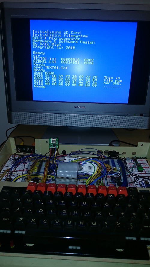
I have been continuing to add to the FAT16 handling software. So now read a directory, showing some attributes (in hex - the length and starting cluster). Also, I can 'open' a file for reading - basically finding the file, and reading the first sector of the first cluster.
These are all baby steps, but I'm not far now from being able to load a whole file in to some area of memory. Being able to do even only this will allow me to write more software on the PC, and save to SD Card for loading by my homebrew.
The screen shot gives a flavour of what is going on from a usability perspective.
![]()
A quick description of what is going on here:
'dir' - obviously displays the directory! But how is quite involved. First, I load up the root directory (which was calculated during initialisation) sector 0. Each 32 byte entry is examined to see if it is a regular 8.3 file. If so, the details of the file are returned for displaying. This carries on until the end of the sector or end of directory. If the sector is exhausted then the next sector has to be loaded and examined. This is because with the 1GB card I formatted using Windows 10, it is reporting that there are 20 sector's work of root directory.
So dir shows two files on the card - TEXT01.TXT, and KERNEL.LST. These are both files I created (in the case of the .TXT) or copied from another directory (in the case of the .LST file). So that tells me that at least the directory structure is being read successfully.
'open' - as you will guess, this opens a file ready for reading. Fundamentally, I reuse the directory scanning routines for dir, but now I am looking for a named file. Once found, I load up various attributes and then load the first sector of the first cluster the file occupies. The approach to do this is fairly involved, but not very complicated once one gets used to it.
'dump' - dumps memory from the location entered. In this case, 0x0300 to 0x4ff happens to be where I have put the raw SD read/write buffer. The dump shows that the open command worked, and is indeed pointing to some content I recognise.
There are a few restrictions which I think I will live with for the moment. One is long filename support. It is quite clever (in my view) how Microsoft added LFN, and not that hard to code up. But for the moment, 8.3 file names are fine. The biggest restriction though is that I will stick with files in the root directory only. This will likely get annoying, but as a means to be able to save and load data, I will stick with it for the moment.
-
Sound
06/14/2015 at 12:58 • 0 commentsFor my homebrew to have a reasonably complete set of features, I really want some sound output capability. For the retro and nostalgic feel, I chose the AY-3-8910. This is a common sound part from the 80s, and was the sound chip in my very first computer, the Oric-1. It was also used in MSX and some other 80s devices (even in PC sound cards and arcade machines iirc).
Wiring up an 8910 is fairly straightforward, however it cannot be driven directly off the 6502 address and data bus. The reason is that the 8910 has some bus control lines which are more compatible with the processor family that General Instrument (makers of this part) also used to produce.
To drive the 2 lines (BDIR, BC1), I have to use some lines from the second 6522. In addition, the data lines also need to be driven off the 6522. This is annoying, because I am having to use 10 of my 16 data lines just to drive the 8910. Also, this is really slow, for example a write sequence looks like this (assuming that X contains the 8910 register to write a value contained in Y:
- Set Port A (this port is connected to the to the 8910 data bus) to output
- Write X to Port A (this puts the register address on to the 8910 data bus)
- Set Port B bit 0 and 1 (these bits are connected to BDIR and BC1 on the 8910) to latch register mode
- Zero the Port B bits to enable the next command
- Write Y to Port A (this is the value we want to set the appropriate register to)
- Set Port B bits to write mode to effect the transfer in to the 8910 register
- Zero the Port B bits ready for the next command
So this is a lot of writes just to set a register in the 8910. And several registers need to be set to be able to make a sound! But I have tiny sense of personal achievement that I'm understanding the challenges that the engineers at Tangerine had when they designed the Oric-1 (similar solution).
One useful thing the 8910 does have 16 I/O ports, so that kind of makes up for having to use the 6522 ports to drive it - although getting data in and out of these ports is slow.
However, these I/O lines will be good for human interface devices as they are much slower than serial or video access. Hence, I am using the port for the 80's Atari compatible joysticks. These need 5 lines (4 directions plus fire button), so I could add more than one joystick (might be useful). For the moment I have stuck with 1 joystick only.
-
Video Output
05/24/2015 at 23:29 • 17 commentsUpdate June 2017
The built in language I have devised (dflat) support VDP capabilities directly such as changing colours, manipulating sprites and setting text vs graphics mode. However it doesn't have any high resolution support and that was ok when I was using the TMS9918, but now that have the TMS9918a variant which supports 256x192 bit map graphics, I thought about how I can access this.
With ROM space tight, I realised that actually I have the ability to do low level access through the commands 'setvdp', 'vpoke' and 'vpeek' - these access the VDP registers, write to VRAM and read from VRAM respectively.
So I wrote a short demo program in dflat which uses the low level access to show how high resolution bitmap graphics can be accessed. The result is in the following video:
Update end-March 2016 : short anecdote..
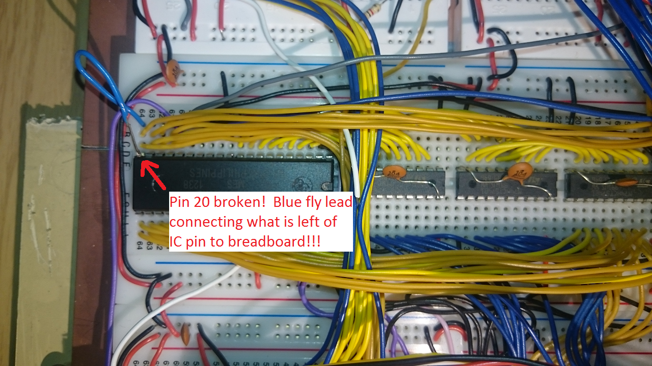
I had a little disaster with the video hardware, although it's ended (sort of ok). The hardware has been working very well for a while so I have been focussing on system and programming language software. However the last time I sat down to do some work, the video output seemed to be going haywire. I won't go through the whole story, but the root cause turned out to be my ground (!) line had broken loose from my USB header. The computer would only fire up if connected to the TV (presumably it was using the TV ground), but the video was messed up. Initially I started prodding about the VDP as breadboard connections can come loose. I pulled the VDP out once or twice in the process of troubleshooting, which is when the disaster occurred - one of the IC legs (pin 20) broke off after one too many insertions and removals. I have a TMS9928 but that doesn't give me composite colour out and I really didn't want to make up a new lead (yet). So I had to carefully solder a fly lead from the just visible connection on the IC for pin 20. See below - amazed that it worked. I think the days of this VDP are numbered and I will start making preparations to install the 9928a. The main difference is that the '28 supports RGB output - but also I am not using the 'a' variant of the 9918 so I will also have access to a full bit-mapped graphics mode.
** Update : The 9928a proved difficult to interface to a monitor with component input (not sure what I was doing wrong) - so decided to install a 9918a, which is the actual variant used on the Ti994/a and first generation MSX computers. **
![]()
As I have previously mentioned, I really needed to have video output for my homebrew that was 80s in style and capability. I poured over a number of options including:
- 6845 as per BBC Micro, Amstrad CPC
- 6847 as per Dragon 32
- Self generated as per ZX80!
The 6845 and 47 to me seemed daunting as my knowledge of digital hardware is so basic, so I discounted those.
I did a fair bit of research in to self generated video - partly inspired by Quinn Dunki's attempt using an AVR. However I didn't have an AVR so was going to use a second W65c02s running at 8MHz - I calculated that I could just about generate a 176 pixel monochrome display if I was very careful with instruction cycle counting. However, I was not sure about the ability to generate the synchronisation signals as this would need something like a 6522 or 6526 and they may not be able to keep up with the display processor. Anyway, to cut a long story short, I decided this option had too many unknowns and I could end up spending a lot of time building something which would not work or ever be expandable.
In my search I did keep going back to the TMS99xx series of Video Display Processors. These were commonly found in the TI99-4/A and MSX range of micros in the 80s, although Colecovision and other consoles also used it IIRC.
The great thing about this VDP is that it as separate video memory, which means my main computer has more to RAM to play with. Also, it has some pretty good features considering it was made in the late 70s including up to 32 sprites, 15 colours and multiple display modes (32x24 column text, 40x24 column text, 64x48 multicolour low res graphics). The 9918 (which I am using) doesn't have the bitmap graphics mode to give pixel level access to a 256x192 grid - if I want this then I could use the 9928a or source a 9918a.
However the TMS99XX series does have some pretty big draw backs. The main one is the fact it is designed to work with DRAMs, which are very hard to get hold of and very fiddly to wire up. The second at the time seemingly minor irritation was the need for a precise 10.738635Mhz crystal.
SRAM replacement for DRAM
The DRAM problem is significant because they are usually accessed very differently to SRAM. Typically an SRAM will have all the address lines required to select an address for reading or writing. A DRAM has RAS and CAS signals which select the row, and then the column - i.e. it is not done in one bus access cycle. The solution to this is something I would never have been able to figure out myself, but basically the RAS and CAS addresses need to be latched so that the full address can be assembled before sending on to the SRAM. The details about how to do this are on the web - in particular an article by Tom LeMense entitled "SRAM Replacement for TMS99x8 VRAM". A quick note about this article though - I downloaded it a few months ago fine, but searching for it now appears to need one to register with n8vem@googlegroups.com.
The implementation principles are as follows:
- Typical SRAMs have the following control lines:
- 14 (A0..A13), 15 (A0..A14) or 16 (A0..A15) address lines depending on whether the chip is 16KB, 32KB or 64KB in size. I use a 32KB chip so have lines A0..A14. However the TMS99xx will only need to assert lines A0..A13, so any additional address lines should be hardwired to ground.
- IO0..IO7 data lines, which are in input mode for write, and output mode for read depending on the three control signals below
- Chip select (CS) - active low. Only when this line is low will the SRAM accept any other control and data signals
- Write enable (WE) - active low. When this line is low, the SRAM will be in write mode (assuming CS is low). The SRAM will take data on IO0..IO7 and write it to the address on A0..A13
- Output enable (OE) - active low. When this line is low *and* WE is high the SRAM will be in read mode (assuming CS is low). The SRAM will output on IO0..IO7 the contents of the memory location defined by A0..13
- The TMS99xx is designed for DRAMs of the time, which had separate lines for read and write as well as lines for address, write, row address and column address. The signals and lines are thus:
- AD0..AD7 lines are to present, row, column and data to be written to ram
- RD0..RD7 lines to read from ram
- RAS, CAS when row and column addresses are present on AD0..AD7
- RW to indicate when data to be written is present on AD0..AD7
- A write sequence is as follows (as shown in the datasheet):
- The AD0..7 lines are first set to the row address, and the RAS line goes low to indicate the row address is valid
- The AD0..7 lines are then set to the column address, and the CAS line goes low to indicate the column address is valid (RAS stays low)
- The AD0..7 lines are then set to the data to write, and the RW line goes low to indicate the data is valid to write (CAS stays low)
- At the end of the sequence, RW goes high, then CAS then RAS.
- A read sequence is similar to above, except that the RW line stays high, and any data read from ram is presented to the RD0..RD7 lines. To enable this, wire IO0..IO7 directly to RD0..RD7.
- Two 74xx574 latches are needed to capture the AD0..7 lines during the row and column sequence, an additional 74xx574 to capture the AD0..7 for data to be written. Let's call them Latch A, B, C
- For all latches, connect the AD0..7 to the D1..8 lines, noting that the TI convention is that AD0 is the MSB and AD7 is the LSB.
- For each latch to capture data presented on its D1..8 lines, the CLK line needs to go from low to high
- For each latch to output the latched data on its Q1..8 lines, the OE line need to go low (the latch will output as long as the OE line is low).
- For latch A, which will capture the row component of the address:
- Feed the TMS99xx RAS line through a NOT gate to Latch A CLK line. The reason for the NOT is because CLK is active high whereas RAS is active low.
- Wire the Q2..8 lines to A0..A6 of the SRAM. Q1 is the MSB and not required as the TMS will output 7 lines of row and 7 lines of column address.
- Hardwire the OE line to ground, to effectively always enable this latch
- For latch B, which will capture the column component of the address:
- Feed the TMS99xx CAS line through a NOT gate to invert the signal. Then feed the inverted through *two* more NOT gates before connecting to the CLK line. This is to provide a small delay between CAS going low, and the data on AD0..AD7 being stable before being latched.
- Wire the Q2..8 lines to A7..A13 of the SRAM (the TMS doesn't use AD0 which is the MSB). Any additional SRAM address lines should be wired to ground (the TMS99xx only used 16KB i.e. 14 address lines in total)
- Hardwire the OE line to ground, to effectively always enable this latch
- For latch C (only used for write operations):
- Invert the RW line through a NOT and feed to the CLK line, to cause the latch to trigger when there is a low to high transition.
- Wire the Q1..8 lines to IO7..IO0 of the SRAM so that data to be written from the TMS99xx is presented to the SRAM. The thing to make sure here is that the wiring from AD0..AD7->D1..D8->Q1->Q8->RD0->RD7 is consistent i.e. there is a path from ADx to RDx. Also, remember this ordering when wiring up the CD0..CD7 lines to the CPU, noting that the LSB is bit 7 and the MSB is bit 0 in TI convention.
- Connect the RW line directly to the OE line so that the latch is only outputting when RW is low (i.e. when there is a write operation being done by the TMS99xx)
- This is pretty much it, except we need to make sure the SRAM is only accepting signals and doing the right operation as follows:
- Connect the SRAM OE to the inverted RW signal i.e. OE will be active low if in read mode
- Connect the SRAM WE directly to the RW signal i.e. WE will be active low in write mode
- Connect the SRAM CS directly to the CAS signal i.e. SRAM will be active once the row and column addresses have been presented.
- So simply, what all this does for a write is:
- TMS puts row address on AD0..AD7
- TMS puts RAS low
- Latch A captures AD0..AD7
- TMS puts column address on AD0..AD7
- TMS puts CAS low
- Latch B captures AD0..AD7
- TMS puts data on AD0..AD7
- TMS puts RW low
- Latch C captures AD0..AD7
- SRAM is active due to CAS being low and in write mode. Latch outputs A and B form the address and latch C output forms the data to be written
- For a read, the final three steps above are not undertaken. SRAM is active due to CAS being low and in read mode. SRAM IO0..IO7 data is output to the TMS.
TMS9918
I acquired a TMS9918 from ebay and infact also have a TMS9929a. They are almost pin compatible, with some key differences in the video output - the 9918 puts out composite whereas the 9929 puts out component video.
Some key features of the this VDP are as follows:
- The clock input consists of XTAL1 and XTAL2 - which need to be out of phase with each other and at 10.738635MHz. This is achived by feeding the 10.7Mhz clock in to a NAND gate to get the inverse. I could have used a NOT gate, but have more 74xx00 chips than 74xx04.
- The chip select lines are /CSR and /CSW. Both high means the VDP is not selected. Only one of /CSR or /CSW can be low at any time. This is achieved by feeding the IO2 output of the decoder and the 6502 R/W line through NAND gates to get the required select states.
- The MODE line selects command or data access to the VDP. As the 6502 is memory mapped, the A0 line is used to select MODE. The effect of this is that the 6502 selects the VDP by accessing memory locationd 0xB400 and 0xB401
There are a number of other small quirks and considerations, but the above are the main ones, aside from the SRAM circuitry, which also complex (for my brain), is still less cumbersome than using DRAMs.
-
Serial Communications
05/24/2015 at 13:43 • 3 commentsSerial Input / Output
One of the key methods of input and output with my home brew is serial communications to and from my development machine (a modern Windows 10 laptop).The serial commmunication protocols I remember from in the 80s and early 90s was RS-232. I naively thought this would be the thing to use now. However, my development machine does not have serial ports - USB is now the only serial methods I have at my disposal.
A bit of research revealed that direct USB to homebrew connectivity would be difficult (at least for me) to achieve. However, the popularity of kit like Arduino and Raspberry Pi have helped the proliferation of USB to serial cables with built in adapters. I purchased a very cheap one off ebay. It means that when connected to my dev machine, an additional COM port in Windows is available, through which I can use a terminal emulator. On the homebrew side, the cable presents 4 pins : +5V, GND, Serial Out, Serial In. This means I also have the ability to power my homebrew off the 5V supply rather than using my home-made 5V supply (interesting mini-project, but clunky).
My original serial comms was designed around using the SP pin on each of the two CIAs for input and output. However, it required a fairly software intensive set up to drive and I wasn't happy with the reliability of it. Plus, I wanted to use the CIA lines for other expansion options.
So I added a CMD 65c51 ACIA. This is a fairly simple to operate serial input/output device, and being part of the MOS family, easy to interface to the 6502. I will keep the rest of this section for historic purposes.
The software programming of the CIA was simple and it was easy to update the few low level I/O routines. However, it still took me ages to get it working because the ACIA needs a 1.8432Mhz clock. As this is not a muliple of my 21.7MHz, it needed it's own clock circuit.
So I obtained an appropriate crystal and wired up a 7404 using a circuit diagram off the internet. I checked it with the scope and it looked like the circuit was putting out a clean 1.8432MHz square wave. However the ACIA was not working, no matter what I did. I then noticed some unusual behaviour - for example if my finger touched the crystal, suddenly the ACIA would work and continue to work. Even putting my hand near the ACIA seemed to kick it in to life - very, very weird.
I put it down to the clock generator circuit. I have not spent any time trying to understand the most analogue part of the home brew which is the clock generators using piezo effects generated by crystals. So I had no idea what to do, but after further searching found an alternative circuit which starts up without requiring the touch of a finger or a magic wave of the hand!!
Old CIA based Serial
The two 6526 CIAs in the system provide serial communications. Even though each CIA has a SP pin for serial input or output, the USB to serial adapter I am using has a dedicated pins for send and receive. I wasn't sure how to wire up a single SP to two pins on the serial interface, so I decided to use one 6525 for input and the other for output.
Serial Input
I started with designing serial input. The mode of operation is as follows:
- Set up the CIA so that PB6 acts as a clock, running at Timer A underflow speed and the SP pin is configured for input
- Connect PB6 to the CNT line which provides the clock for sampling the serial input line
- Connect the /FLAG pin to the Serial input line. This means I an configure an interrupt to occur if the serial line goes low. The default state of the serial input line is high, with a zero start-bit indicating the start of a transfer.
The software to run this is fairly simple. In pseudo code it looks like this:
- Wait for /FLAG to go low (this can be through an interrupt or polling the CIA ICR)
- Wait 1/2 a bit time - this is to try and sample in the middle of a serial bit
- Initialise Timer A to 1/2 the bit time required and start in continuous mode, PB6 to toggle Timer A underflow. At this point the CIA is starts shifting serial data on the SP pin in to the SDR
- Monitor the ICR to indicate SP (meaning that the SDR now has 8 bits of data).
- Read the SDR - et voila, this is your received byte.
One slight complication - the CIA expects data to be shifted in from MSB to LSB (i.e. shifting right each time). It turns out the USB to serial adapter does it the other way. So the final step is to shift the SDR LSB first in to the translated byte MSB first.
The Timer A countdown is clocked by Phi2, which is 2,684,659Hz. This means one clock cycle is approximately 0.3725 of a microsecond. To clock serial data in at 9600 baud (bits per second) means that each bit is approximately 104 microseconds. Half a bit time is 52 microseconds. Therefore Timer A needs to be set to 140 (52/0.3725, rounded to the nearest whole).
Serial Output
Output is done on the second CIA, and the mode of operation is even simpler than input:
- Set up the CIA so that the SP pin is in output mode, with Timer A set up for 1/2 the bit time
- Write to the SDR (first translate the byte to be sent as due to the MSB vs LSB shift order)
- Monitor the ICR SP flag until the CIA indicates the data has been shifted out
-
Software Design
05/16/2015 at 18:11 • 0 commentsMonitor
I have updated my monitor program, with some additional commands and it is more of a command line style rather than single letter commands:
Command Description DIR Directory listing
LOAD <addr> <file> Load from address <addr> the file <file> OPEN <file> Open the file <file> and output to the current output device MEMTYPE V | M Set memory type to VRAM (V) or normal memory (M) all memory commandsact on this memory typeSET <addr> <xx>* Set the memory from address <addr> to bytes defined in <xx>. A sequence ofmore than one byte can be written.
DUMP <addr> Dumps 8 byte blocks from address <addr> with an ASCII readout. Enter continuesthe dump for another 8 byte block, any other key stops the dump.
WATCH <addr>* Watches the memory at <addr>, outputting bytes to the output device until anykey is pressed. More than one address can be watched.
SECTOR <addr> Load sector <addr> in to memory. Useful for low level inspection of SD cards. -
Hardware Design
05/16/2015 at 18:10 • 0 commentsIn terms of hardware design, I realised that there are not really that many parameters one can play with when using off the shelf components. The point is that things like the 6502, 6526, 6522, 9918 etc. are by design expecting certain inputs and outputs, so they set out some fundamental design constaints.
The general input, output and interfacing capabilities provided by the 6522s (two of them) and the memory map design are the two most significant areas for creativity.
NEW Memory Map
For the old memory map, see that heading.
The reason for this new section is that I had the old memory map running since basically the beginning, and has served well for more than a couple of years. So why change it? Well, a number of reasons:
- I have a 128K RAM chip and 64K ROM chip
- Old memory map only addresses 48K of RAM and then minus 4K window for memory mapped IO
- Old memory map only addresses 16K of ROM
- Less than 1K of ROM remaining, limiting further ideas for functionality such as extending the interpreter (more hi-res commands, floating point support) and OS (better support for FAT, bigger cards etc.)
So I went ahead and came up with a new memory map with the following features:
- Smaller IO window of 1K still supporting 8 devices in 128 byte sections
- Any write to ROM space will write to the shadow RAM at the same address
- Ability to disable ROM to get full read and write access to RAM across whole 64K (except IO window of course)
- Ability to map top 32K of RAM to any 4 positions in RAM, so having access to all 128K
- Ability to map top 16K ROM access to any 4 positions in ROM, so having access to all 16K
The way I have done this is to take spare lines from the two 6522s I have, one will be ROM disable, two will be to select the RAM bank and the other two to select the ROM bank. The actual decode logic is in the downloads.
I now have plenty of opportunity to expand my project, especially so with the additional ROM space.
However although the hardware is done, I need to reorganise the software radically for example:
- One cannot simply change from one ROM bank to another, it would be pulling the rug from underneath the CPU. It has to be organised so that the CPU is still executing expected code after a switch. The easiest way to do this is have common switching routines across all ROM banks
The new decoding logic is available to view in the downloads section. It will take a while to reorganise the software though e.g.:
- Create a new common section
- Determine what banks will have what responsibilities e.g. BIOS, File System, Interpreter, Graphics, Sound, Utilities
- Rebuild the make file to assemble images in to a 64K ROM (at the moment I am simply copying the same 16K four times, so I have no extra usable ROM space)
It will take a little thinking through but once implemented, I will have loads of available ROM to fill - should keep me busy with the project for a many more months!
OLD Memory Map
The memory map was one of the first and most interesting areas of investigation. The 6502 has a 64KB address range - so all my RAM, ROM and memory-mapped devices need to fit in to that. Being old-school, I wanted to try and put together a map which maximised RAM without overly compromising ROM and memory-mapped device access.
In the very early incarnations of the homebrew, copied the simplest address decoding approaches I found in other designs:
- If A15 is zero, then select RAM
- If A15 is one and A14 is one then select ROM
- if A15 is one and A14 is zero then select devices
So this gives 32KB RAM, 16KB ROM and 16KB devices space. I had a board working with this configuration, but it was just to allow me to prove I had wired things up.
I went for an addressing scheme which would give me 44KB RAM, 4KB devices (8 512 byte IO blocks) and 16KB ROM. It was fun coming up with the decoding logic for this and then working out how to implement this using some NAND and NOT gates.
Section Type Address Range Decode rule A15-A12 (binary) A ROM 0xc000 - 0xffff Between 1111 - 1100 B IO Blocks 0xb000 - 0xbfff 1011 only C RAM 0x0000 - 0xafff Between 1010 - 0000 The decoding of these address line (A15 to A12 for the section select, A11 to A09 for the IO block select) needs also to take in to account the chip select lines available. Doing this would hopefully reduce the complexity of the decoding a little. I am using a W27C512 for ROM, 628128 for RAM and a 74xx138 3 to 8 decoder for the IO block select. These chips have the following select lines:
- ROM : /CE, /OE
- IO BLOCK (74xx138) : /E1, /E2, E3
- RAM : /CS1, CS2
In addition to the A15-A12 lines, the additional signals are also needed from the 6502:
- PHI2 (this is low when the 6502 has control of the data and address lines)
- R/W (this is high when performing a read, else it is a write)
The analysis I did resulted in the following table, which showed that I need 3 NOT and 6 NAND gates to implement the decode (plus the direct use of A14 which doesn't need a gate). I am sure someone can do better than, this but hey this is is my first custom memory map decoder, and it seems to work, so I'm happy - but any suggestions would be interesting. Note that Gate #1 Input A did have Phi2, but this is wrong, I don't need Phi2 to supply the RMO and IO decoder select - this is why my 6522 didn't work as I was not allowing devices to be selected until Phi2 was already high, whereas most 65xx family devices need the chip select to be activated before Phi2 goes high. Gate #6 is still correct - RAM must not be selected when Phi2 is low incase of inadvertent writes before address lines have become valid.
Gate # Type Input A Input B Output 1 NAND +5V A15 ROM /OE, IO /E1 2 NOT A14 3 NAND A13 A12 4 NOT Gate #3 IO E3 5 NAND A15 A14 6 NAND Phi2 Gate #5 RAM /CS1 7 NAND A15 Gate #2 8 NOT Gate #7 9 NAND Gate #8 Gate #4 RAM CS2 10 NAND A14 R/W ROM /CE In addition, A14 feeds directly to /E2 for the IO decoder, and in addition to the chip select lines for RAM, the 6502 R/W line feeds directly to the /WE line (i.e. low for write, high for read).
Device Selection
As mentioned, the /E1, E2 and E3 outputs enable the 74xx138 decoder. This basically then takes A11, A10, A09 as inputs and selects one of 8 outputs (active low). So therefore I have 8 addressable devices I can select. This should be plenty, as I can't think of more than 8 different devices:
- Block 0 (0xb000) : 1st 6522 VIA
- Block 1 (0xb200) : 2nd 6522 VIA
- Block 2 (0xb400) : TMS9918 VDP
- Block 3 (0xb600) : 6551 ACIA (planned - low priority as I already have functional serial I/O)
I had hoped to make the AY-3-8910 a memory mapped device, but this is not going to be directly accessible due to the very long strobe and hold times that the datasheet is specifying. So this will be through the 2nd 6522 Port A for data transfer, two lines from port B to control access).
-
The Basics
05/16/2015 at 10:21 • 0 commentsAlthough this is an on-going project, I have been working on it for over a year before publishing anything, so I'll try and capture some of my approach, experiences and lessons learnt to bring this site up to date.
One thing I have been doing over the life of this project is trying to do it on a shoe-string budget. That's just the way I am - a bit of a tight-arse who likes to think he's got a bargain of some sort! However whilst being budget conscious is great in nearly any setting, it has to be with some level of pragmatic trade off and risking the saying of 'buy cheap, buy twice' coming in to effect. So I learned by trial and error the right budget trade off! I don't know how much I have spent on this hobby, but I am sure it has to be approaching £250-300 by now.
In the beginning..
I started off with literally nothing - no components, no tools, no experience. But I did a lot of reading. The internet is fantastic, so many people willing to put their experience and knowledge out there on the web for the rest of us to benefit from. I can't possibly remember or list every resource I have examined, but over the course of this project www.6502.org has been a fantastic well of knowledge.
Initially I needed to get some kit together. I bought a bunch of basic components (resistors, capacitors, transistors, 555 timers, crytals, LEDs etc.) with some wire (solid core, multi-colour). I also decide to use breadboards to try out my experiments (as they were right at the beginning). I love breadboards, but I'll mention some of the problems I have with them later, they're not all good!
Despite working in IT professional services - where I often have to spend weeks or months architecting and designing solutions - I spent virtually no time thinking about the design features of my computer (perhaps it was a back-lash to my day job!). I had some key features in mind, some mandatory otherwise it wouldn't be a functional computer, and some that I wanted to make it useful. What useful meant was the ability to program some 1980s style rudimentary video games, complete with sound effects. So the features:
- It had to have a CPU (!), a 6502 one (see below)
- It had to have memory (!), but how much I hadn't decided
- It had to have some IO (!), but for what purposes I hadn't decided
- It had to have video graphics output. I had homebrews which used small LCD panels or no video at all - this wouldn't for me as I wanted to be able to play video games on it!
- It had to have sound output output. Again, I had seen homebrews which didn't care much about sound, but I wanted this.
CPU
So, I had some basic electronic components, but no complex ICs like a CPU, memory etc. Looking through a number of existing homebrew sites, I could see a variety of CPUs had been used including 6809, 8080, 68000.
However fascinating these other projects were, I had already resolved to use the 6502 at the heart of my project. The reason is straightforward nostalgia. My first computer was a 6502 based micro called the Oric-1, bought for £80 in a knock down sale in 1984. I was 13, and knew nothing about computing, but convinced my hard-up parents that I needed one, and this was in the right price bracket (i.e. really, really cheap). But this computer took me from never having written a BASIC program to being able to code assembly in hex (because I couldn't afford an assembler - eventually wrote one for myself). When I grew out of the Oric-1, I got an Atari 800XL in 1985, which was also 6502 based.
Aside from nostalgia, I could see that with everything else I was going to have to learn to be able to build my own computer, having something I was already familiar with would be a good thing.
The first one I bought was off ebay (where most of my acquisitions of components etc. were made) - a CMOS based Rockwell model. However, during my investigations, I also found out that a company called the Western Design Center was still producing 6502 CPUs which could operate at much higher clock speeds than the original 1-2MHz in the 80s. For this main reason, I ended up using a WDC 6502 piece (there is a story behind why I thought I needed the higher clock speeds - will go in to that in another log).
Memory
Choosing RAM was straightforward enough. On ebay UK, there are a couple of sellers who provide 'hombrew computer kits'. These kits provide a CPU (typically a Z80), some glue chips (typically PLDs) some support chips (video, RS232, IO), some ROM and some RAM.
The supplied RAM is typically SRAM and the ROM is typically EEPROM. Neither SRAM nor EEPROM were very common in 80s microcomputers. However, DRAMs are difficult to both obtain and use - DRAMs need refesh circuitry which would add complexity (6502 has no refresh capability built in, although I understand the Z80 may well have). So I decided that in the interests of pragmatism, SRAM would be fine - I'm not trying to recreate a 100% 80's replica.
The supplied ROM is typically EEPROM. However, before purchasing one of these kits, I had decided that I would buy some EPROMs, a very cheap multi-format PROM programmer and a basic UV eraser. This is because of experience with my first job after graduating, working as an embedded systems programmer. In this job I would burn EPROMs and erase with a UV unit - I figured this would be how I would do things in 2014! Anyway, I will cut a long story short, due to the unreliability of probably 10+ year old EPROMs and the long build/burn/erase cycles, I turned to EEPROM. The so-called multi-programmer I had couldn't burn EEPROM, so I had to invest in some proper German (and so expensive - around £130) kit that I could rely on.
I/O
Without I/O there is no point to a computer of course. So I had decided originally that a 6522 (ebay sourced) would be fine with an RS-232 interface for serial comms. What I didn't do was to realise that RS-232 was a pain due to the voltage differences and the fact that my modern computer doesn't even have RS-232! I was also unaware that the 6522 serial capabilities are both flawed and limited, so that I may have to 'bit bang' the I/O without some kind of serial interface IC like a 6551. In the end, I ditched the 6522 in favour of two 6526 (close relation to the 6522) out of a non-working C64. At the time I didn't have access to a 6551 so had to do a bit of funky wiring to get that working. Although I will add a 6551 at some point, it is working well enough for now so it will be a lower priority than things like sound.
However, the serial data capabilities on my development PC (modern laptop running Win7) only suppports high speed USB. I had to buy a USB serial adaptor cable - which are commonly used for Arduino development. Not expensive - less than £3.
The 6526s together currently provide the following functions:
- TImer A in both 6526s is used for the serial input output timing. When I get a working 6551 in, this timer will become free
- In 6526-1, all 8 bits of Port A are used to enable the keyboard row and column addressing
- In 6526-1, 3 bits of Port B are used to control the leds on the BBC keyboard
- In 6526-1, 1 bit of Port B is used to sense the key pressed for a row and column
- In 6526-1, /FLAG is used to sense when serial input is available. Will become when I used a 6551
- In 6526-2, all 8 bits of Port A are needed to provide a bi-directional databus to communicate with the sound chip
- In 6526-2, 2 bits of Port B are needed to control the select signals to the sound chip
- In 6526-2, /FLAG used to sense when the BBC keyboard hardware strobe senses some key has been pressed.
When I use a 6551, then I will move the keyboard signal from 6526-2 to 6526-1. What way all keyboard access is through a single CIA (somehow feels a bit neater / elegant, although has no material effect on the code structure!).
I have now replaced the 6526 based I/O with an ACIA. And also added a keyboard from an old BBC Micro. The BBC Micro keyboard is actually very cool - it has some basic circuitry which means it scans for a key press in hardware, generating a flag which can be then used to cause an interrupt. The interrupt service routine then needs to check each row and column - but this is really fast and does not need to be done very often (relative to a 2.7MHz 6502!), so a whole key scan is not done any more often than 0.05 of a second (3 vertical blank intervals).
Further update - as noted elsewhere, I found that he 6526s are not reliable at 2.68Mhz - in nearly everything they appeared to operate as expected. Only when I was trying to read the joystick inputs from the AY-3-8910 was it clear something was wrong. After some confusing with chip select and Phi2 timing, I have managed to replace the 6526s with 65c22s - so now everything works fine at 2.68Mhz.
VideoOne thing I have observed with many homebrews is the lack of video output - they get by with serial I/O only or interfacing to hex LED or dot matrix LCD panels. This would not be enough for my needs, as I wanted something which would be able to drive a TV, ideally with graphics capabilities to render simple games.
A reason for lack of video on many homebrews is that old graphic chips are hard to design for (at least for someone of my low level of expertise) and hard to come by. Modern graphics chips are way too complex to be able to interface to my homebrew - and totally would dilute the 80s feel that I was after.
I looked at a number of options. One of the early options was to 'bit bang' video! Yes, I calculated that if I drove the 6502 at 8MHz, I could probably drive a display with about 176 pixels horizontal resolution. Anyway, I didn't spend too much time on it - the cycle counting was critical and even if the display did work, there was absolutely no room for future expansion (e.g. colour, sprites, resolution). I was partly inspired by Quinn Dunki (see http://quinndunki.com/blondihacks/?p=955) - although she was using an ATmega and outputting VGA, so it was a much more sophisticated bit bang solution than mine. So, due to effort vs limited reward, I ditched that approach [Edit - there are cleverer ways to use the 6502 address lines to generate video signals, but would have required additional logic which I never considered and got too complicated to generate colour etc.]
Next, I looked at 6845 chips. These were used in a few popular computers in the 80s including the BBC Micro and Amstrad CPC. A highly configurable chip, but it still needed a bunch of supporting electronics (character ROMs and additional custom logic for colour) - it just looked too complicated for someone of my limited experience.
So finally, I settled on the Texas Instruments 99xx VDP, as used in the MSX computers of the early to mid 80s. I acquired both the TMS9918 and TMS9928a - almost pin compatible but the '28 produced component video whereas the '18 provides composite. These are great graphics chips for their era (late 70s) - however the integrated nature comes with a big con. They are design with the assumption that they connect to DRAM. As I mentioned before, DRAM is a pain and hard to get hold of - and it was one of the reasons why I was originally put off by using the TMS99xx. But there are so many clever people willing to share their knowledge, and I found a resource on the web to adapt SRAM for use with TMS99xx VDPs - a fantastic write up by Tom LeMense entitled "SRAM Replacement for TMS99x8 VRAM".
Sound
I have added an AY-3-8910 made by General Instruments for sound. This is another nostalgic chip for me as it made an appearance in my first home computer, the Oric-1. I've described more about it in the sound blog. I will use the 10 input/output lines to add 2 joysticks (each joystick needs 4 direction signals plus the fire button).
65c02 Homebrew Computer on breadboard
Custom designed breadboard computer (BBC!) with bespoke programming language, full graphics, sound and SD card storage.
 Initial decoding logic - don't even ask me what I was thinking! This has definitely not made it through to the current set up, in fact I never got to using it as realised it had impractical (or at the least worrying) levels of delay due to the number of cascading chips I was using.
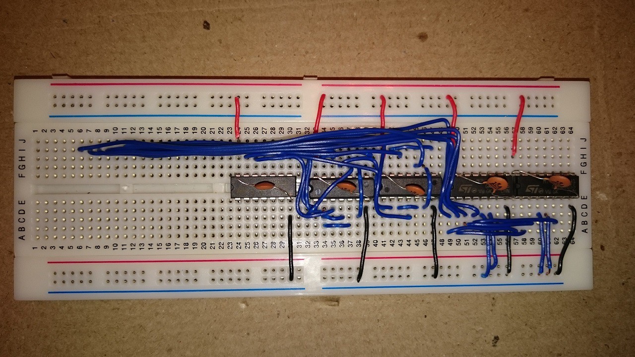 When I got hold of a TMS9918, I tried to work out if it was alive with a little free-run circuit. All it proves is that the TMS is getting power and a valid 10.738Mhz clock signal, so not really that useful with hindsight..
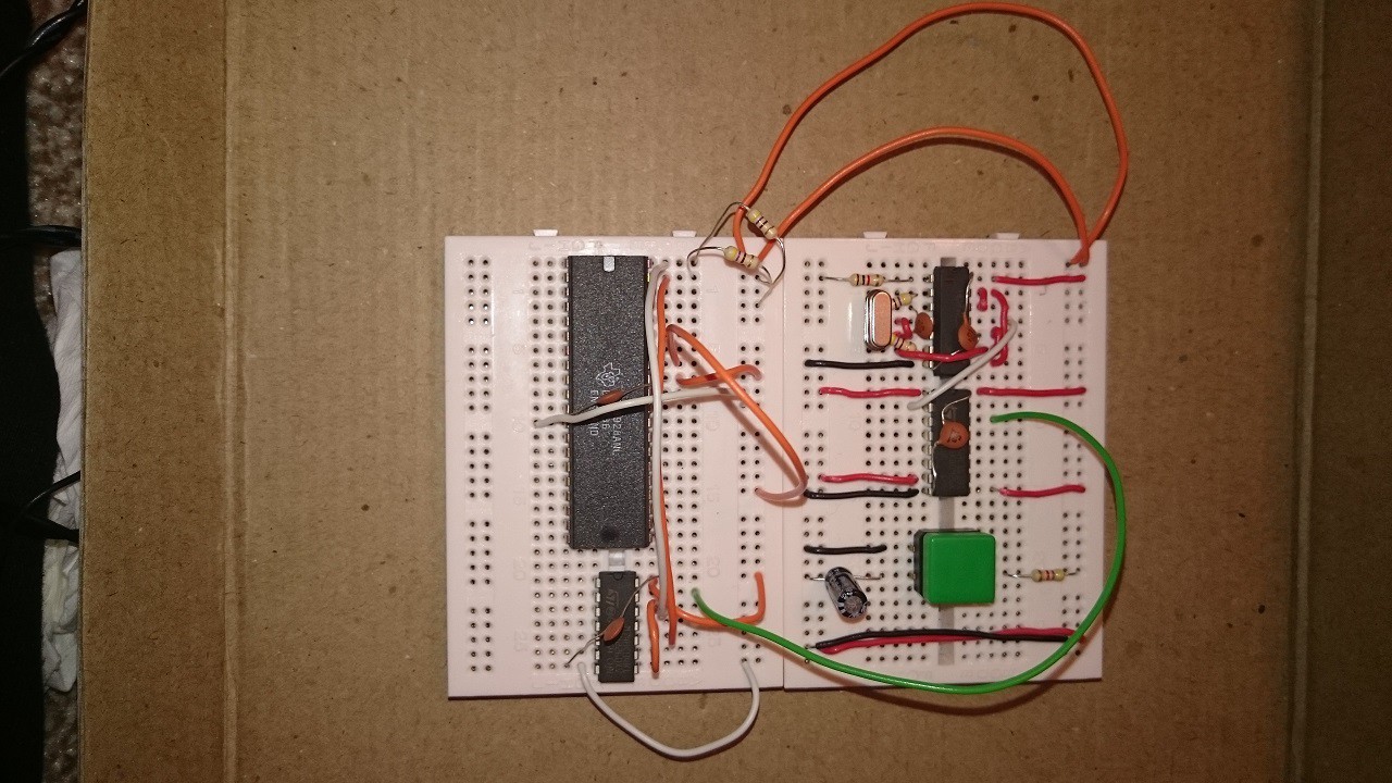
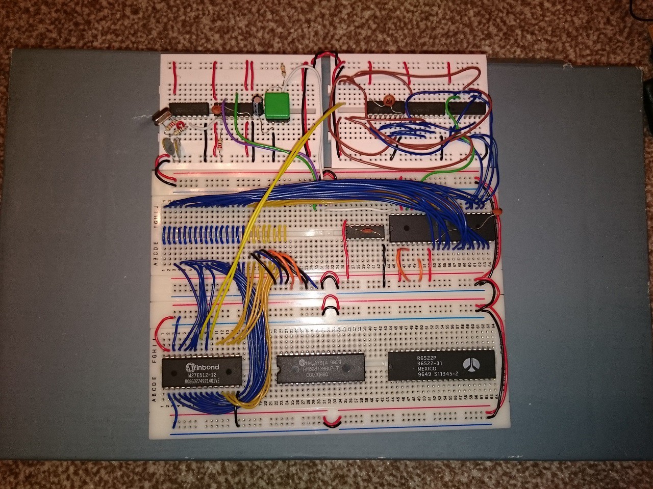 Talking about oscilloscopes, I thought I shoud put up the core tools I used (and still do). First the oscilloscope. I had a 2Mhz bandwidth handheld puppy, but it was inadequate so invested in a USB connected one with dual channels. Without this I definitely would not have got the board running with all the components I have today.
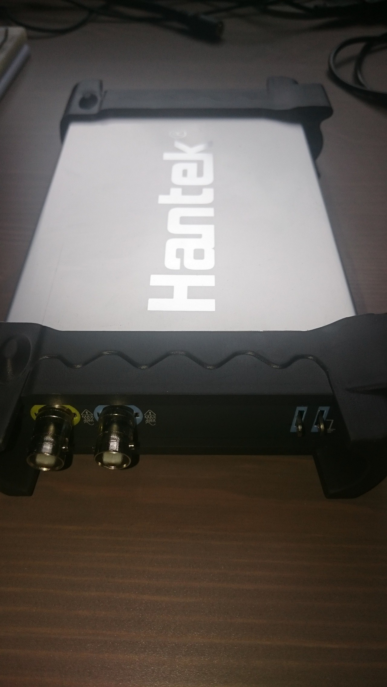 Next, I have a EEPROM programmer. I did try to go down the authentic route and got myself some EPROMS, programmer and UV eraser! The edit/program/test/erase cycle was depressing so quickly moved on to the BATUPO - I tried some cheap far-East programmers (Top-Win anyone?) but this was and is way more reliable. This is now the most used tool of course as it's all about the software..
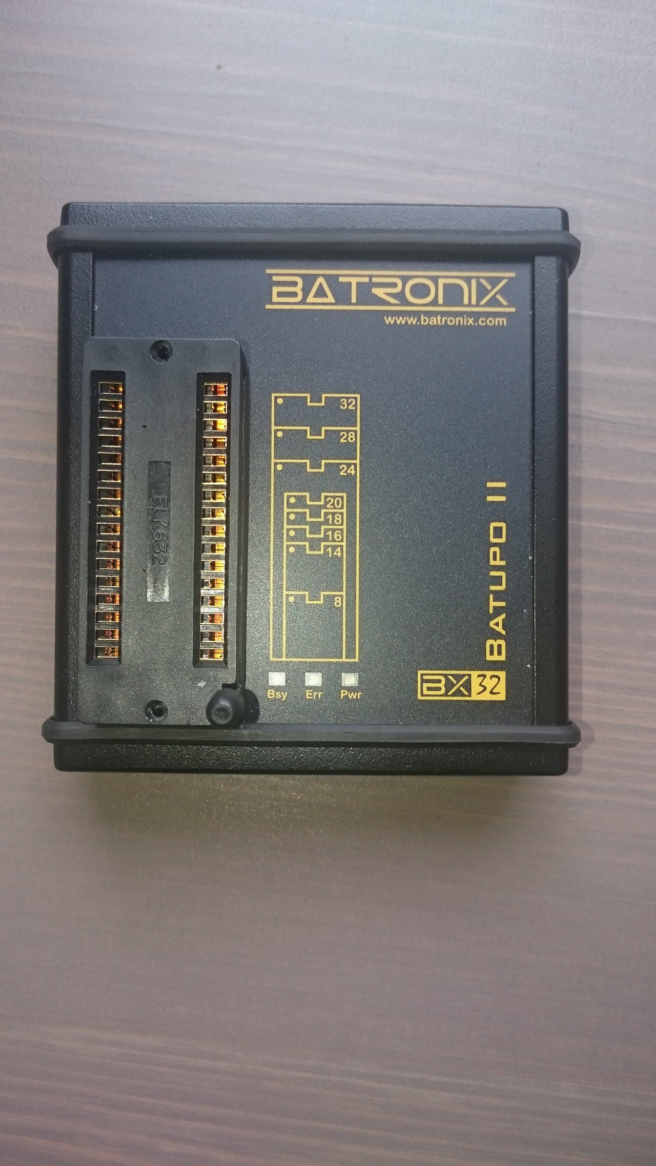 The other thing I needed was a TV capture device. For a while this worked fine, but the delay on this is horrible, so now am using a regular LCD TV (as I have space in the office because we moved to a larger place in Summer 2015). Still, the TV Out was useful initially when office and desk space was at a premium.
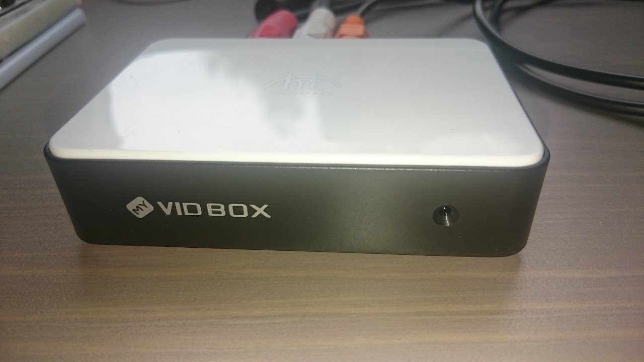 I ran out of USB ports - Programme, Scope, TV Capture. And that didn't leave room for a serial port! So I needed a USB hub.
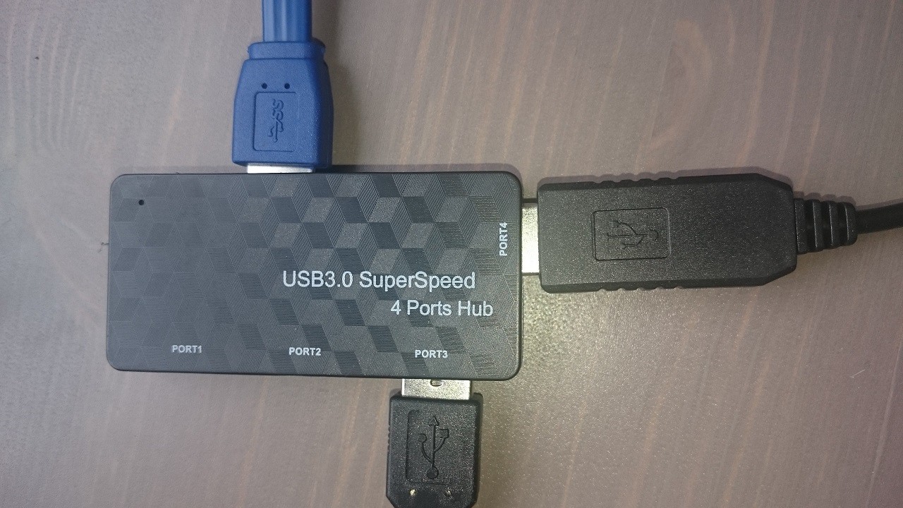 My initial board was serial only using the 6526 (from a non-function CBM64) to bit-bang the serial line. I managed to get 9600bps reliably, before deciding to do things more properly and implement a 6551 ACIA. The board in this pic has ROM, RAM, 6502, 6526 all working well, with serial I/O the only means of communication. Even so, there is quite a lot of breadboard building up here, and it is starting to get awkward / delicate in moving it.
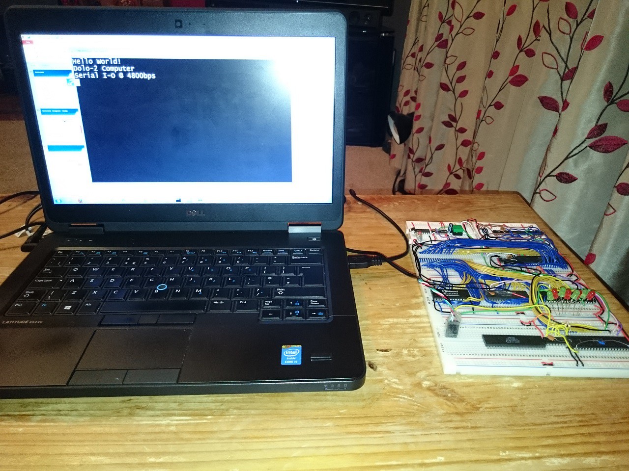 I sent the following picture to my friend (sadly he passed away too young) when I was explaining the basics of what I had got going. The breadboards are now stuck to a plastic chopping board to keep them together! This is very much the current set up, but with sound added and the IO chips are actually 6522 VIAs rather than 6526 PIAs. The original clock and reset circuit is bottom left.
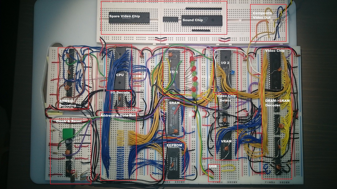 More recent pics to follow..