 Jithin
The very first board .
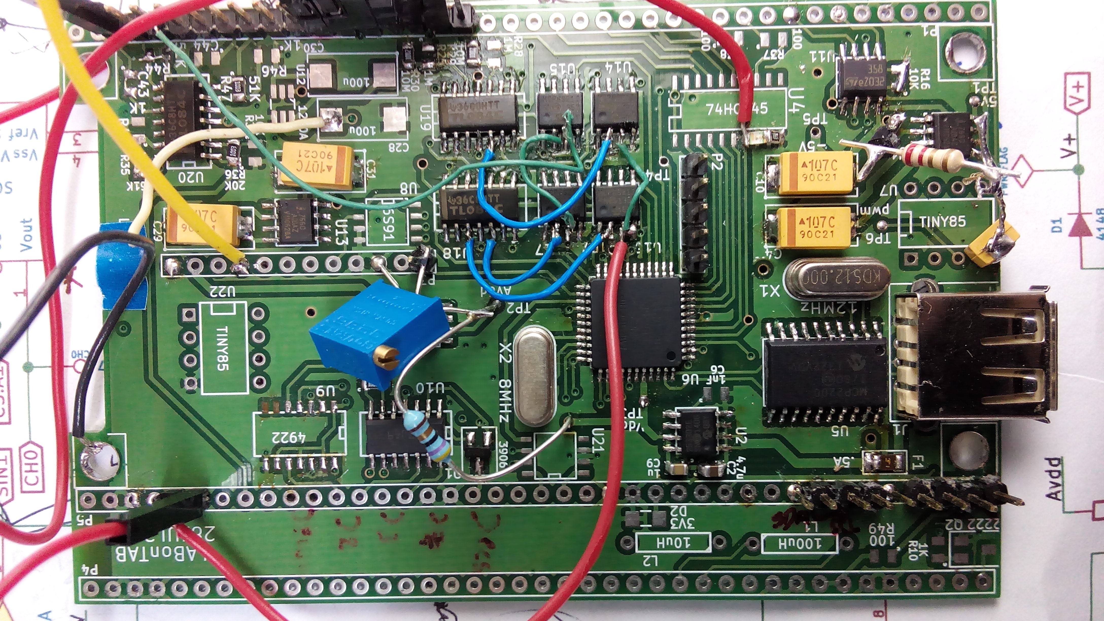
A lot of patchwork went into this
Rough list of features:
- USB powered. .5mA polymer fuse. MCP2200 convertor.
- Controlled by PIC24E
- MCP1725 LDO regulator
- REF196 stable 3.3V voltage reference
- bipolar power supplies generated by 7660 and 1240A charge pumps
- MCP4922 2-channel DAC for programmable voltage and current sources
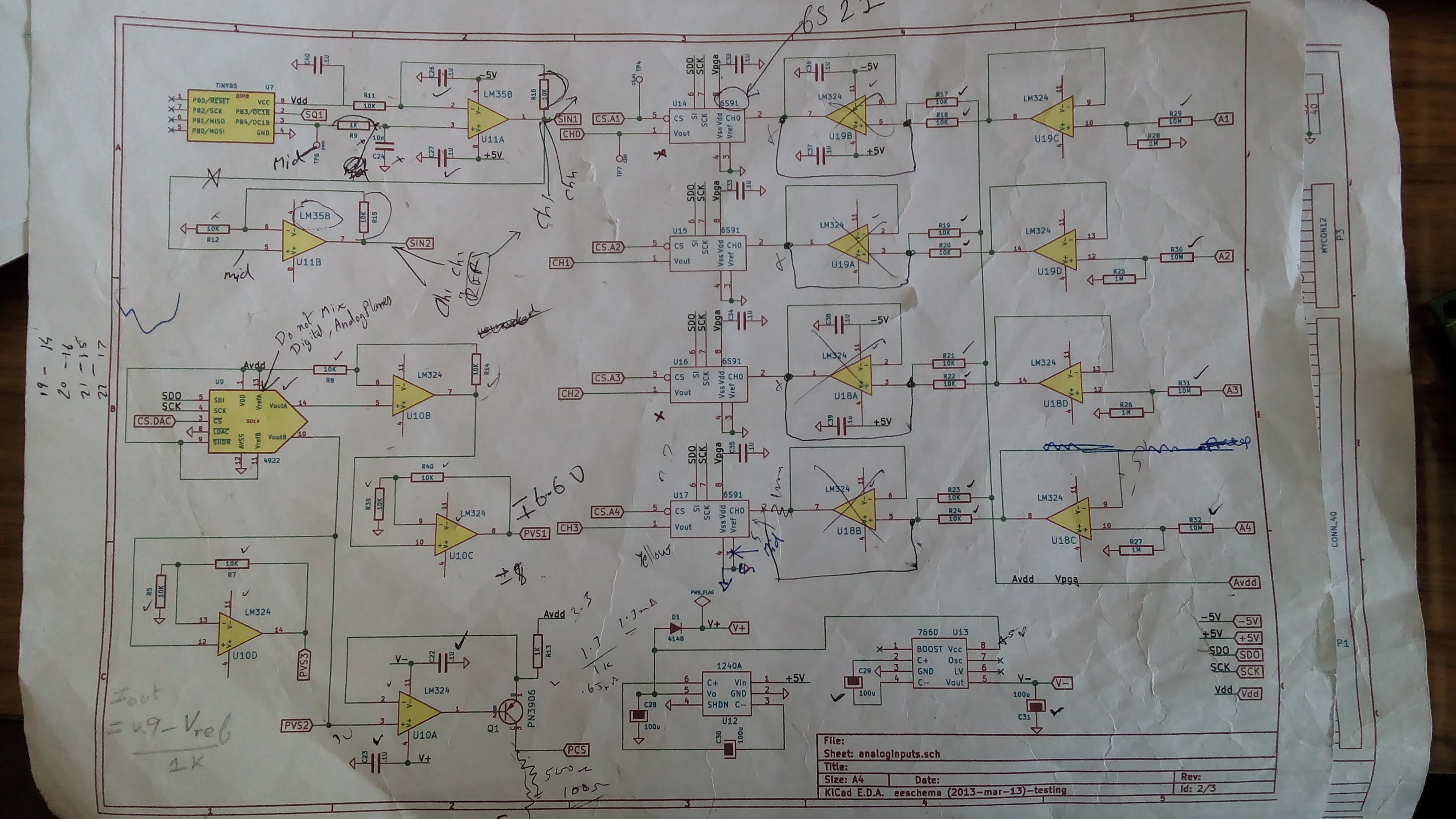
- MCP6S21 programmable gain amplifiers to provide several software configurable input ranges for voltmeters and oscilloscopes.
- 4-channel oscilloscope. +/- 16V full range. +/-500mV at 32x PGA gain.
- ATTINY based sine wave generator
- Capacitance measurement via CTMU of PIC24E
- Digital I/O
- Component store - A collection of commonly used resistors, capacitors, diodes etc soldered directly on the PCB, and broken out into a berg strip for quickly trying out stuff.
Errors and concerns that decided the design of the next iteration
- The voltage reference of the PGA needed to be set to the midpoint. LM324 buffered midpoint references were added.
- Quality of ATTINY generated sine wave was rather poor. I found a low priced alternative, PIC1572, which not only ran faster, but also had 3 16-bit PWMs, and a 5-bit DAC which could be used to add more programmable voltage and current sources.
- Planned to use two PIC1572 to the next iteration for generating dual sine waves. Made the mistake of assuming the outputs would be phase correlated since they were identical. :/
- Ripple noise from charge pumps needed additional filtering.
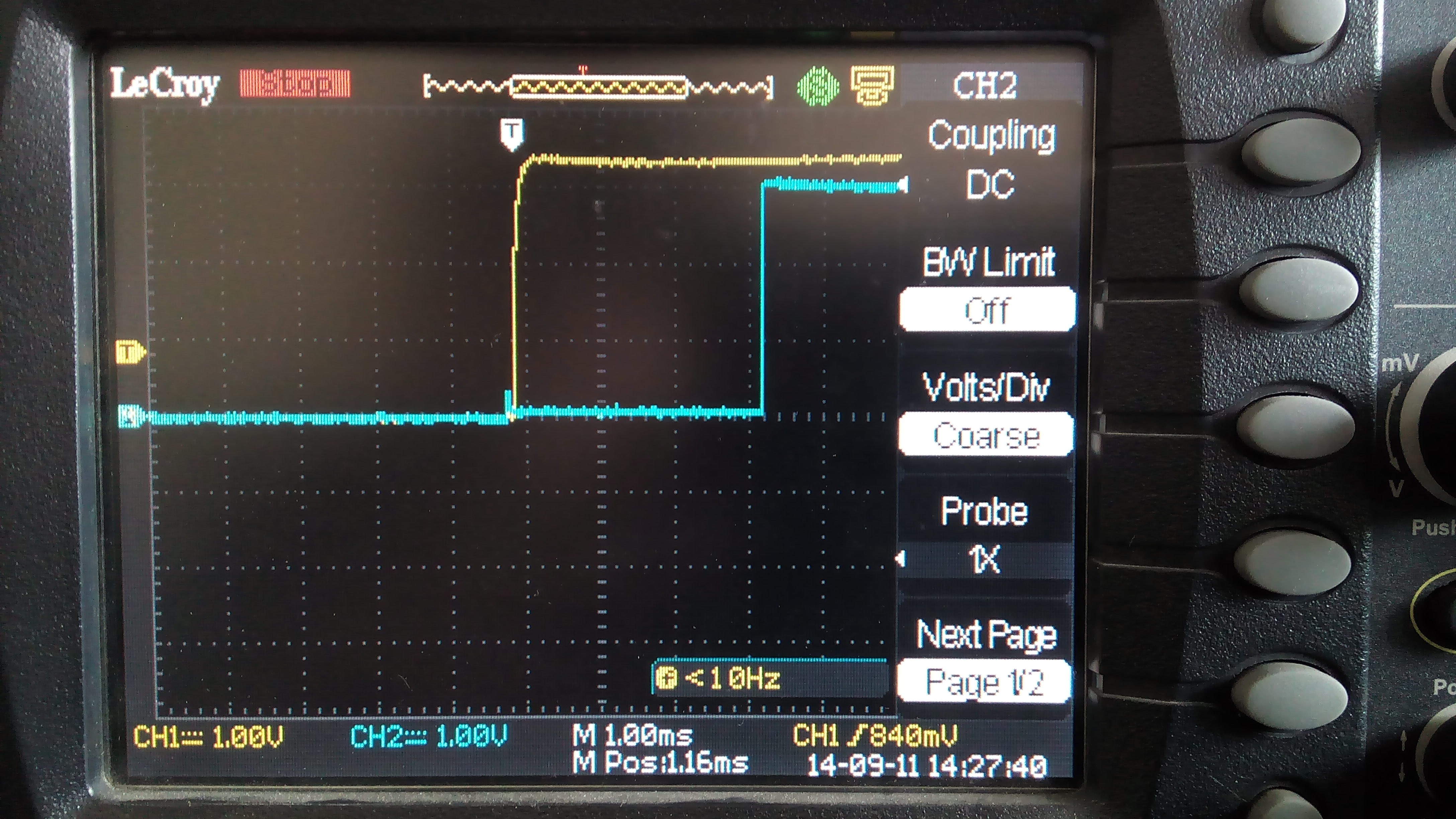
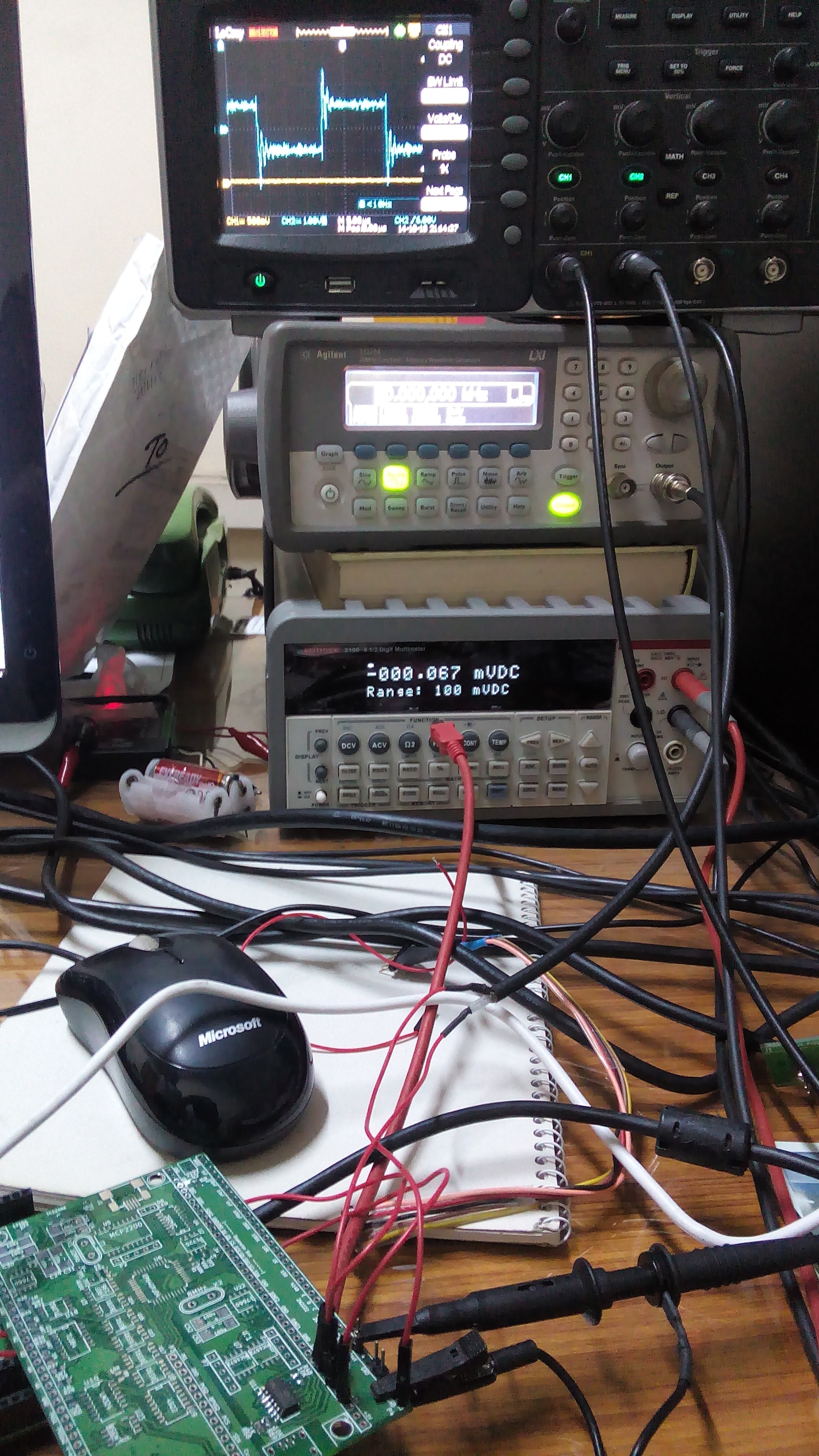
- PIC24E refused to START . I had powered Vdd from the MCP1725, and Avdd from the REF196 for separating analog and digital sections. After much hunting around, I found that Avdd and Vdd must never be more than 300mV apart or else the oscillator won't start. I tried to delay the Vdd rising speed by trying out several capacitors attached to its Delay pin, but with no luck. Here's a screenshot detailing how the Vdd(blue) and AVdd(yellow) voltages would rise on power up
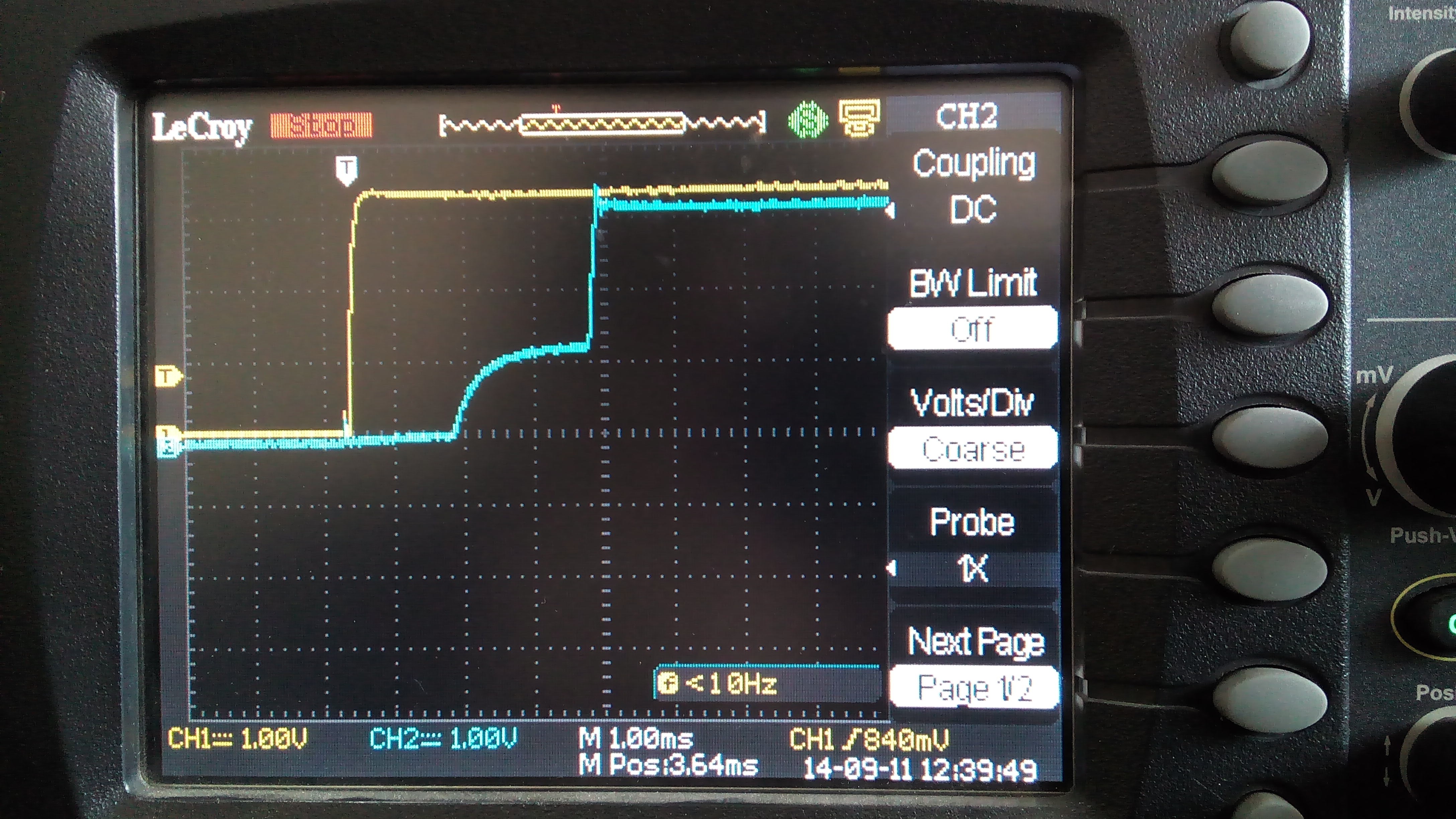
The Cdelay Pin of 1725 was attached to a 1nF cap.
Noise Levels
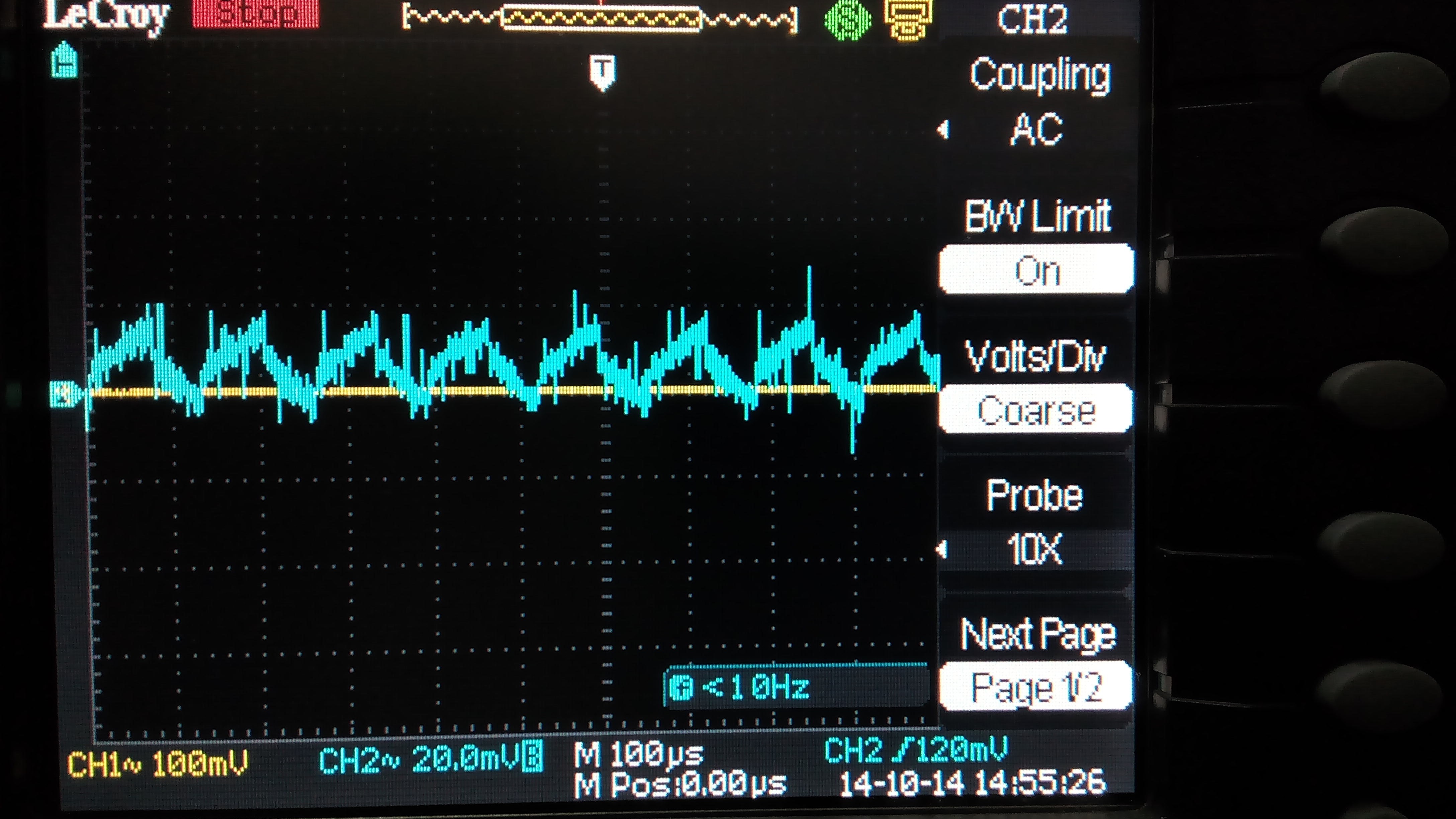
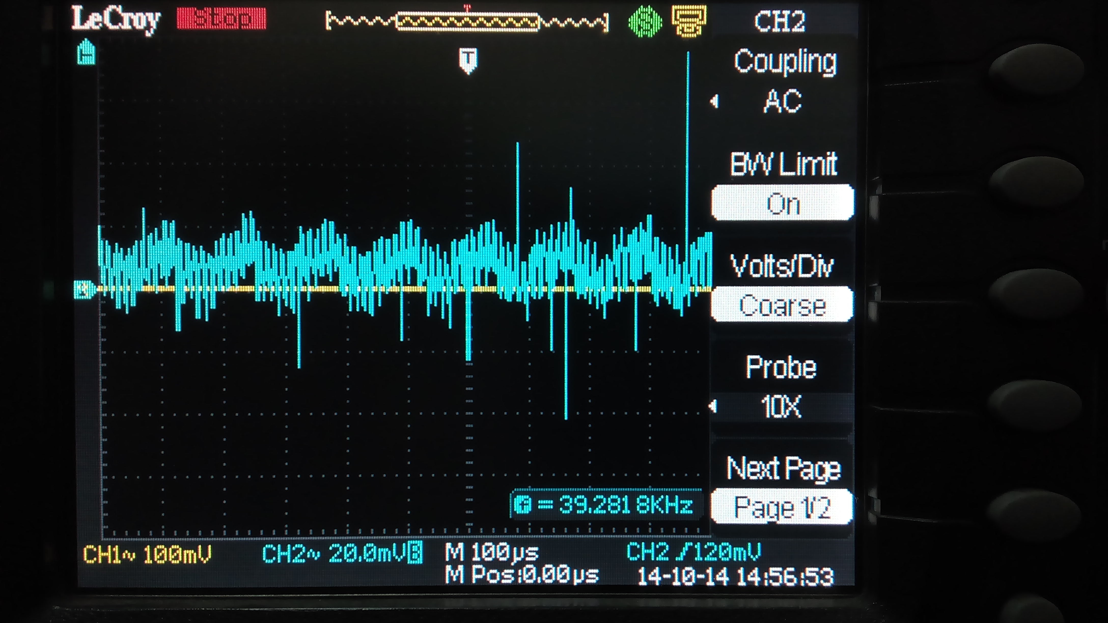 Positive power supply (+10V voltage doubler) ripple level with a 680 ohm load.
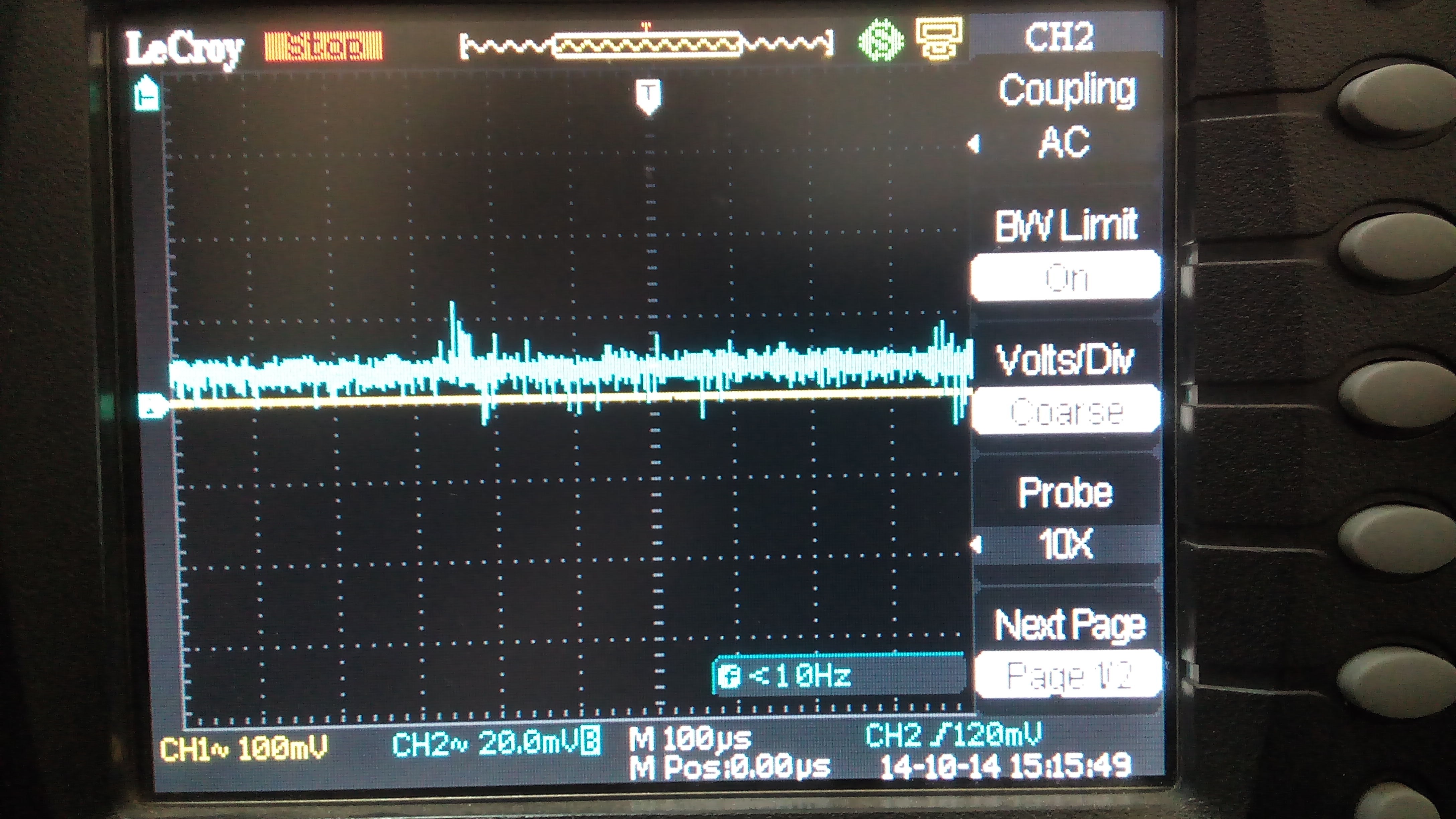
Attempting to Clean noise with RC filters
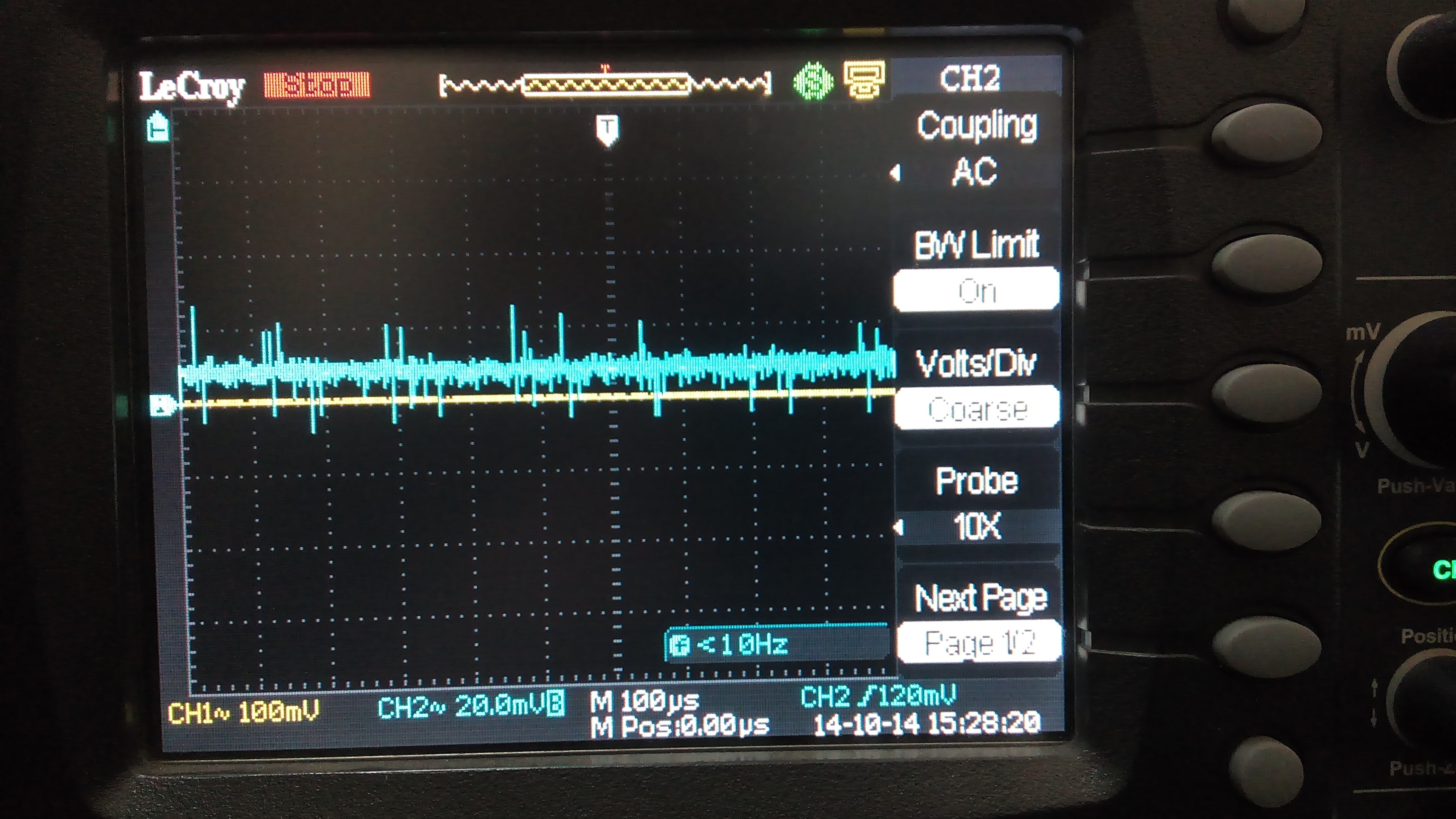 25 uF, 47Ohm RC filter applied to +10V
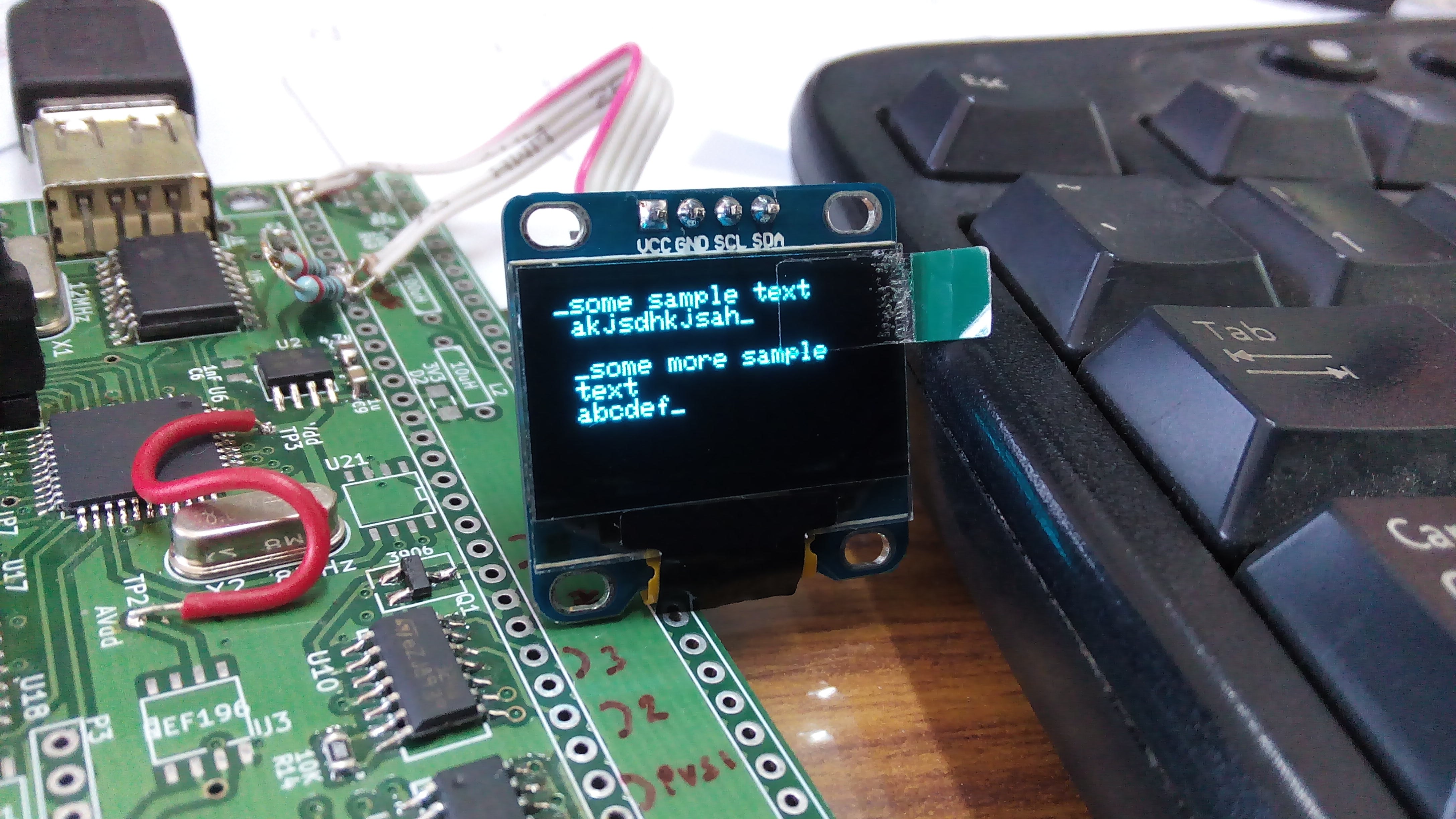
Tested I2C with SSD1306 OLED display
Testing an inverted configuration op-amp for input voltage range. Overshoot with oscillations occurs if frequency compensation isn't set up.
Discussions
Become a Hackaday.io Member
Create an account to leave a comment. Already have an account? Log In.