Close
0%
0%

Tern - Ternary Logic Circuits

A series of ternary logic gates and higher level components implemented in the real world.

Similar projects worth following
Moore's law isn't permanent. It's already falling behind. Eventually physics will throw a wrench in the works of ever-shrinking photolithography techniques and something else will have to contribute to satisfying the worlds demand for greater computational power. It doesn't look like quantum computing will be ready in the next few decades, so ternary computing might just bridge the gap.

This project documents physical implementations of ternary logic gates and higher level sequential components. By documenting functional techniques for building up the lower level components of a ternary processor I hope to ease the way for others to begin experimenting as well.

By ternary I mean a circuit can output three distinct voltage levels and can accept and decode those same voltage levels.

A shout out to [ThunderSqueak] who inspired my interest in the subject with her earlier work in the area and her talk at the Hackaday 10th anniversary meetup.

Please note: The project log really is a log. I add an update for virtually every change of any value whatsoever. Sometimes I add updates of no value whatsoever. Because.

If you just look at the most recent log updates it will not make a lot of sense because I have had to borrow or evolve the nomenclature for a physical implementation of ternary circuits and because I am not describing a finished product. I am describing an ongoing process complete with wrong turns, errors, conclusions, and solutions. The best way to view this project is from the beginning.
TernaryMOSFETSK-XRev1.pdf

Adobe Portable Document Format - 132.25 kB - 07/04/2016 at 04:55

Preview

TernaryMOSFETS9-HRev1.pdf

Adobe Portable Document Format - 128.80 kB - 07/03/2016 at 09:27

Preview

TernaryMOSFETS1-8Rev3.pdf

Adobe Portable Document Format - 123.03 kB - 07/03/2016 at 09:27

Preview

TernaryMOSFETS1-8Rev1.pdf

Adobe Portable Document Format - 177.92 kB - 07/02/2016 at 07:39

Preview

SumRev2.pdf

Adobe Portable Document Format - 99.49 kB - 06/13/2016 at 03:59

Preview

View all 41 files

  • Project Gracefully Terminated

    Mechanical Advantage04/18/2019 at 06:34 0 comments

    I am officially ending this project and beginning a new one called the Ternary Computing Menagerie.

    The purpose of this project was to educate myself while making proof of concept balanced ternary combinational and sequential logic gates. Mission accomplished! 

    Furthermore, other projects running parallel to mine, such as the Homebrew Ternary Computer and Shared Silicon have also demonstrated proof of concept circuits at the board level and in silicon.

    At this point I have shifted my attention to higher level applications of ternary logic and math to start filling in the gap of knowledge about how having three states will affect algorithms, tritwise operations, primitive data types, instruction set architectures, etc. The ternary computing menagerie is my collection point for all such research.

    The Tern project will remain here for anyone interested. My recommendation is to read the logs in sequence.

  • Sum Gate Solved

    Mechanical Advantage07/05/2016 at 17:27 0 comments

    The crazy behavior of the Sum gate's power draw is officially solved. By building up the circuit piece by piece and keeping my eye on the current draw continually, I was able to narrow the problem down quite a bit. It only occurred with the inputs in particular positions, and only when power was first applied to the circuit. This sounded an awful lot like latchup so I figured I must be applying too much current to one or more input pins. Playing around with resistor positions and values didn't solve the problem, but with some [insert preferred search engine here]ing around I ran across a great little document here from Analog Devices. It is entitled "Winning the Battle Against Latchup in CMOS Analog Switches" and it clued me in to another way you can get latchup.

    As we all know, one should not exceed any of the absolute maximum values listed in a devices datasheet. As far as I could tell, I was not exceeding any maximums, but I hadn't taken time or relative maximums into account. Some values in the datasheet are dependent on others, and the one tripping me up was the maximum allowable voltage on an analog input. The highest voltage on an input is equal to the supply voltage. But on initial power up, which one gets power first? In my case, apparently it was the analog input, thus making that voltage higher than the supply voltage which hadn't quite gotten up to speed yet. Therefor I was exceeding maximums and the device latched up causing a low impedance connection between the input and the power rail. Voila!

    The solution? This is covered quite nicely in the document as well and consists of nothing more than placing a schottky diode in line with the power pin of the analog switch. I don't quite follow why this works (magic probably) but it does the trick.

    Along the way I also tweaked a lot of resistor values to bring the overall current draw to between 14 and 18 mA depending on what the two inputs are set to. I want to fiddle around with this a bit more to see if I can reduce that further and then I will post a revised schematic.

  • Final Ternary Monadic Gates Using MOSFET's

    Mechanical Advantage07/04/2016 at 04:57 0 comments

    Here are the gates from K through X using only MOSFET's.

  • More Ternary MOSFET gates

    Mechanical Advantage07/03/2016 at 09:32 0 comments

    Here is the next set of ternary MOSFET gates.

    And here is an updated schematic for gates 1-8. It just corrects a few resistor values.

    Interestingly, no ternary gate requires more than three transistors. How tautological.

  • Another Rabbit Hole

    Mechanical Advantage07/02/2016 at 08:02 0 comments

    <Sigh>. I got sidetracked again by accidentally discovering how to do everything I've already done in a totally new way. I have recreated and tested every ternary monadic gate using only discrete transistors and accompanying passives. I don't even need the +1V and -1V references for these. Now I know for a fact that there is no technical reason why ternary gates cannot be miniaturized and implemented in silicon. It would be an old non-CMOS process, but it would work. I worked up the first eight gates so here they are. I'll post the remaining gates when I get a chance to document them. Then back to rebuilding a Sum gate that doesn't shoot itself in the foot.

    On a related note, I also took a second look at a project called the Trimux that I had previously disregard as being pseudo-ternary. I had misunderstood that it accepted binary inputs and had ternary outputs. Now that I look at it more carefully, I find that it really is ternary and more elegant than any of my existing techniques in many ways. It is based on pass-transistor logic (which I've already implemented slightly in my Flip-Flap-Flop and ill-fated Sum gate) and quite simple. I'm looking forward to plagiarizing shamelessly ;)

  • Keeping Current

    Mechanical Advantage06/23/2016 at 08:54 0 comments

    I've been engaged in a detailed analysis of current consumption by various ternary gates in different configurations so as to better understand why the Sum gate was drawing so much current. I've concluded that by drawing more current than the wall wart could supply it became damaged which resulted in the crazy measurements I was getting right before it died permanently.

    Since then I've been studying how much current is drawn by different configurations of the ternary gates such as with different pull-up, or pull-middle resistors, different resistors on the input pins, terminating or not terminating unused comparators on an IC and so forth. Over 160 individual measurements so far. The conclusion I'm coming to so far is that I should have been using larger resistors for my pull-ups and pull-middles, and that I should not have been neglecting resistors on the comparator inputs. The LM393 comparators and discrete transistors don't have any difference in current draw by adding input resistors, but the LM319's have a significant difference. This doesn't fully explain how I was drawing over 200 mA with just six components and no short circuits, but I'll just have to build up the Sum gate again, keeping track of current consumption as I power and connect each device.

  • Request For Help

    Mechanical Advantage06/15/2016 at 07:02 2 comments

    Okay, now that I've killed a power supply, its time to get a professional opinion. I've been trying to track down why my sum gate (rev 2) consumes so much power. While poking around and checking how much power different components consume I saw ridiculous numbers like a 393 comparator pulling over 400 mA, then suddenly changing to around 130 mA, then jumping up to 200 mA. That's just one example. I even tried swapping out IC's to make sure it wasn't a bad component. While checking this all out I detected a faint burning smell (uh oh) and quickly confirmed that every component on the board and my DC/DC converter were cool to the touch. No dice; it was the wall wart giving up the ghost.

    My components are as seen in the SumRev2.pdf file and my DC/DC converter is this little module. My +5v, GND, and -5v lines come directly from its outputs. I've also got two simple resistor dividers providing the -1v and +1v references, but I'm sure that isn't the problem because they are only used for high impedance comparator inputs. Does anybody see anything in my schematic that would explain the crazy power consumption? Thanks much if you can help!

    Oh yeah. I tried adding all the appropriate bypass caps (not shown in the schematic) out of a primitive urge to perform a magic ritual where knowledge was lacking. As expected, it didn't work.

  • Updated Sum Gate

    Mechanical Advantage06/13/2016 at 03:59 0 comments

    I finished testing more possible ways to use transistors rather than comparators to build up monadic ternary gates and did find a few more than I had before but none of them were of use in simplifying the Sum gate. I did however find an error (a transistor source attached to ground instead of +5V), make the diagram a bit more clear, and add the truth table.

    So here it is.

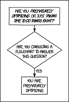
  • Thoughts On Premature Optimization

    Mechanical Advantage06/10/2016 at 01:30 0 comments

    An XKCD comic got me thinking recently... that may be the nerdiest thing I've ever written.

    My general plan has been to create working versions of the ternary gates necessary to eventually build something that actually performs a real function. Specifically, I wanted to build a device that would compute the Fibonacci sequence to three trits. I have now proved the functionality of every component that would be needed to do exactly that.

    At the same time, I have been testing various types of transistors as replacements for the simplest of the ternary monadic gates; those ones which have only two possible outputs. I already posted one schematic that simplifies some of the monadic gates, but have realized that there are more possible simplifications to be made in that area. I've just received a delivery of more depletion mode transistors to test.

    Finally, I've also been checking out current draw in these circuits and was surprised to see over 200mA being used by the Sum gate. I need to go through the different circuits I've already built and tweak the resistor values to bring that down to something more reasonable and while I'm at it, I might as well add bypass caps to all the schematics in the appropriate locations.

    So basically I'm looking at a considerable amount of testing, iterating existing circuits and verifying the improvements, and documenting the improved circuits. All this before I've actually built anything beyond solderless breadboard prototypes. In other words, premature optimization.

    Instead, I think I'll finish testing the transistors, use that data to improve the Sum gate if possible, document it, and then build a three-trit adder with three position switch inputs and LED outputs. This is a much more modest first-build than the Fibonacci idea, and as such, is a lot more likely to get done. And I hope to do it on a real board through Oshpark. If it all works out it will be my first PCB design.

  • Face Palm

    Mechanical Advantage06/05/2016 at 05:59 0 comments

    After going through the trouble of drawing up the schematic for the new improved Sum gate you'd think I would actually post it.

    Here it is!

View all 69 project logs

Enjoy this project?

Share

Discussions

Andreas wrote 12/10/2016 at 21:11 point

Very cool project! Maybe you have already read it, but I have found this 192 page report to be very interesting: http://xyzzy.freeshell.org/trinary/

  Are you sure? yes | no

Mechanical Advantage wrote 12/16/2016 at 05:54 point

Yep! That was one of many reports I pored over. They did some really good work, but failed to explain a couple of totally vital points that made it impossible to repeat their work. That said, I did pick up a few tips from them that helped me avoid some early pitfalls.

  Are you sure? yes | no

theo.j.sandstrom wrote 07/15/2016 at 20:45 point

Hey, looking at the flip-flop, I was kind of confused. Could I see a truth table? With the clock line, how have you used all three states? It seems like it is essentially a pseudo-ternary flip-flop, as the clock line only uses 2 states. Would it make sense to have + clock one trit of data and - clock a separate trit, so that it is essentially 2 flip-flops in one, and actually uses all three states? Or would this still be pseudo-ternary, because each individual flip-flop has only 2 states? I guess it is difficult to implement in true ternary, because you are either writing or you are not. How are you working around this?

  Are you sure? yes | no

Mechanical Advantage wrote 07/27/2016 at 08:42 point

Ah yes, I drew that before I learned to be a bit more explicit about what each sub-circuit was doing. I'll walk you through it really quick.

I am assuming a normal on/off binary clock or a simple enable line. However, the sub-circuit that the clock and/or enable line goes into is ternary tolerant, meaning that you can pass any of my three logic values to it and it will interpret it as intended. Specifically it is set up as a 2-gate. That means it will accept any ternary input. A - will result in a +, a 0 will result in a -, and a + will result in a - as well. This is because the pass transistor chip that it is controlling (DG201B) is active-low. Therefore, passing a 0 or a + to the enable line will enable the flip-flap-flop to accept a new value. Leaving it at - will prevent a change of state.

I've done  quite a lot of thought-experiment type work with ternary clocks, and I haven't been able to see much added value in a simple system. In more complex systems with pipelining, multi-threading, etc. it *might* add some value.

The reset line is also ternary tolerant and is also set up as a 2-gate. It's arranged such that a 0 or + will reset the Flip-Flap-Flop to 0 regardless of whatever is going on with the enable or input lines.

The DG201B is just a signal routing station for the various signals, the two comparators with positive feedback loops are the "storage" portion of the circuit, and the final comparator and diode logic on the back end are the output stage that clamps the output to the appropriate levels. There is a bit more details on the back end in my final two posts on the design of the FFF.

I'll admit it's not as elegant as a binary Flip-Flop, but then again, a binary Flip-Flop doesn't look particularly elegant either if you look past the pretty logic diagram and actually check out the circuit.

While some might think this is "pseudo-ternary" I disagree. The circuit is capable of stably storing any of three different logic levels without any DRAM style analog tricks like using capacitors to store the state and just refreshing them really fast. The Enable and Reset front-end circuitry is tolerant of ternary inputs, but only have two states in themselves. This is because three states were unnecessary, not because they were impossible. I contend that binary is a useful *subset* of ternary and it should be used where more than two states are not needed. After all, what would the third state for "enable" be? I only need two; enabled, and not enabled. Adding a third option would have been a solution in search of a problem.

Thanks for the interest; I appreciate being able to bounce these ideas off another person instead of just running thought experiments in my head.

  Are you sure? yes | no

theo.j.sandstrom wrote 07/27/2016 at 12:25 point

OK, thanks for the clarification. I guess things like clock and enable are inherently binary in their very nature. It's cool that it still accepts ternary inputs though. Keep up the great work with ternary logic. I've found this really interesting. 

  Are you sure? yes | no

Zach Smith wrote 04/27/2016 at 00:22 point

The reason the Russians had made ternary computers was because they required less vacuum tubes to do the same amount of logic. When transistors were invented binary became easier to produce.

I've done my own investigation into ternary as of late last year. It is possible. Although setting it up with current C-MOS (The most popular transistors used in computers to date.) it would require a constant power supply and a 3rd power rail. Also the current C-MOS configurations used in binary circuits will not work because of this third power rail.

ThunderSqueak seams to have figured it out but I ran into a brick wall getting MOSFETs to reset to a "3rd" value.

If you are interested... PM me. I have some details I would be willing to share with you.

  Are you sure? yes | no

Martin wrote 03/16/2016 at 08:24 point

I cant see how this ternary logic can help to increase computing power. While you can - of course - calculate in a base-3 number system, logic gets difficult: Yes/No/I-don't-know? The different gates look way more complicated than our typical CMOS gates.

  Are you sure? yes | no

Mechanical Advantage wrote 03/17/2016 at 08:17 point

The fact is, no-one knows; myself included. In the 60's and 70's the Russians built quite a few ternary computers which were acknowledged by western computer scientists to be superior in both computing power (though how they measured this is unknown to me) and price. Unfortunately the "party" didn't approve and they were all dismantled and I've never found a schematic or component list. It also doesn't have much relevance to todays chip fabrication techniques. Yes, most gates are more expensive in terms of transistors, but interconnects would take up far less room. That's a big problem in integrated circuit design since the cost of a chip is largely based on its physical size (assuming the chips you are comparing use the same photolithography process).

The way one would normally assess "computing power" is if it performs specified tasks faster for a given clock speed. But even assuming the same clock speed is touchy. Ternary circuits need to handle three distinct voltage levels with buffer areas between them. To accommodate this greater "bandwidth" you would either need to increase process size, or decrease clock speed, or increase power consumption. Theres a lot of trade-offs implied there and only building such a chip (or doing some really good simulation) would let you decide if any of those trade-offs are are worth the potential increase in computing power that ternary logic could bring.

Right now I just want to further the development of the area, not try to push on anyone that its really a better choice. No-one can honestly say one way or the other. Some examples:

1) Nobody has figured out a carry look-ahead adder in balanced ternary, only ripple-carry. This is a total deal-breaker because ripple-carry is an 0(n) problem but carry look-ahead is an 0(log n) problem. There's at least one very knowledgeable person actively working on solving this problem but it hasn't been achieved yet.

2) Some mathematical functions are far easier in balanced ternary. 2's complement binary requires an inversion and an addition to change the sign, but in balanced ternary changing the sign is a simple inversion. In balanced ternary rounding and truncation are the same operation.

3) In balanced ternary you can identify the sign of a number merely by the value of it's most significant non-zero trit. No 1's complement, no 2's complement, no sign-magnitude, and definitely no wasted operations switching back and forth and converting and checking signs, etc. A fairly large chunk of signed-number related processor cycles just disappears and gets replaced with a simple comparison function that can be done in one clock cycle.

4) Tritwise operators! You know all the crazy sorcery that compiler writers and low-level programmers do with bitwise operations to implement high-speed algorithms, shortcut difficult problems and shave off clock cycles here and there? Well in binary they are limited to only a few operators and still perform magic with them. In ternary, there are almost twenty thousand two-input tritwise operators! Sure, most of them will be of little use, but it would take decades to sort that out. If I had a functioning ternary processor of even the most elementary sort, the first thing I would do is turn it over to some compiler writers or CS/math wizards and ask them to play with tritwise operations. There's no telling what algorithms could be implemented more efficiently with that kind of freedom.

5) The logic actually isn't that complicated. The more I work with it, the more I see that having a third state is really beneficial. Because the logical assignment of meaning is performed by the human, not the hardware, you can choose that third state to mean whatever you decide is most valuable in your context. Some rational options are; don't know, don't care, doesn't matter, save for later, or you can "clamp" the third state to be equivalent to either of the other two.

Long story short; development has to be done to even evaluate if this is a good idea or not, but there is a lot of potential.

  Are you sure? yes | no

Similar Projects

Does this project spark your interest?

Become a member to follow this project and never miss any updates