-
A Reliable Sum Gate... Finally.
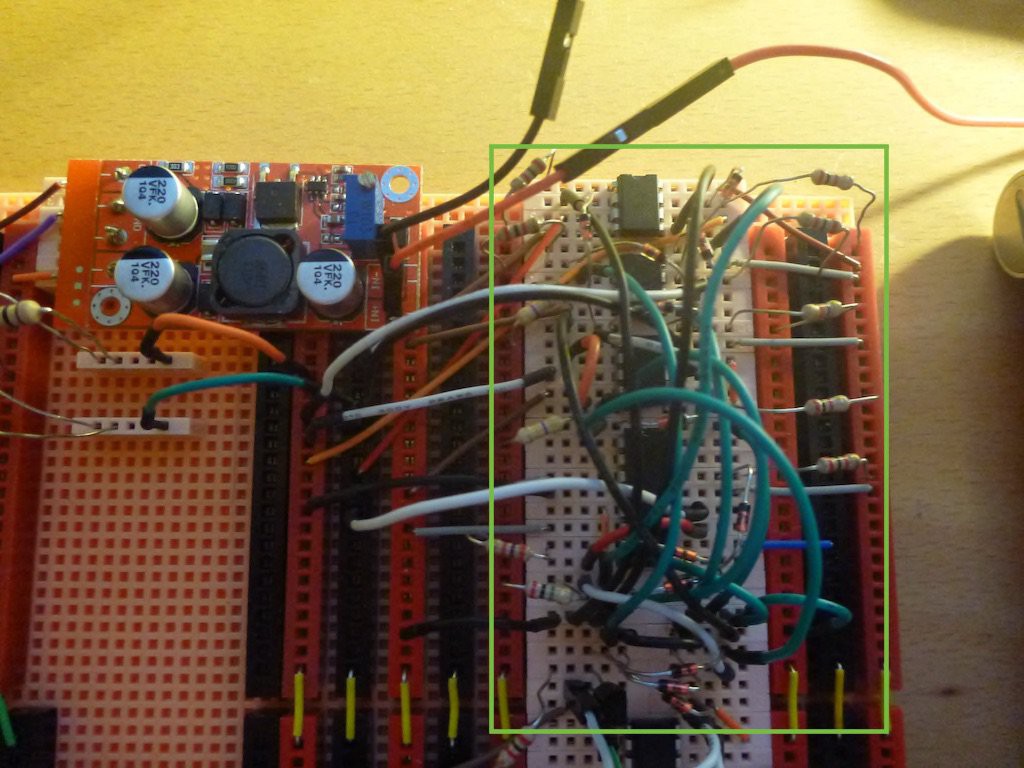
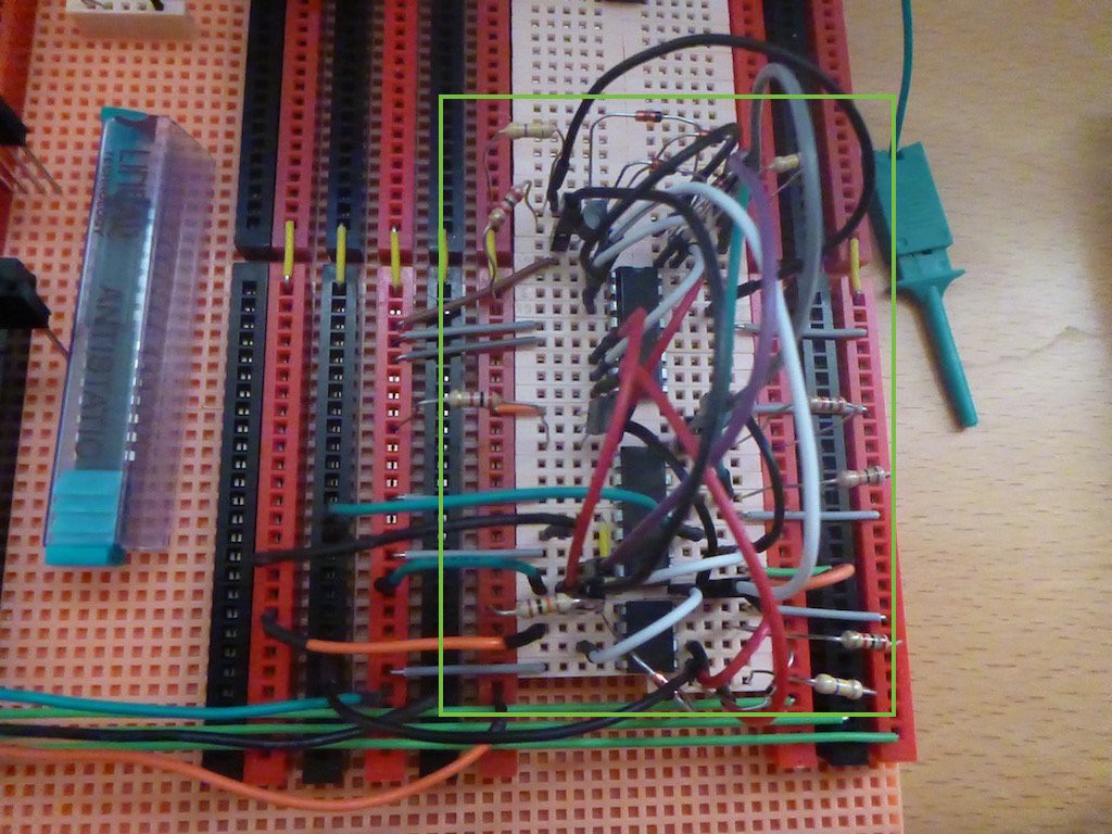
06/04/2016 at 08:03 • 0 commentsAfter much trial and tribulation I have finally finished a really functional Ternary Sum gate. Following are two pictures. The first is the prior incarnation of the Sum gate that barely functioned. The second is the slightly simpler and entirely reliable Sum gate.
Here's the awful one:
![Awful Sum Gate]()
And the one that actually works:
![]()
As mentioned before, the output is the 1-trit sum of two input trits. The carry is handled by the Consensus gate which has already been published previously. That means I now have every ingredient necessary to produce a ternary ripple-carry adder. However, at this level of integration it won't be trivial. The Sum gates still take a surprising amount of board space. Both of the two pictures above were the result of compacting the components down so that every single row was utilized. The final result still takes up a 1/2 sized solderless breadboard for a single gate.
The improvements in functionality are due to the fact that I replaced most of the diode logic with pass transistors. This would have increased the footprint of the gate, but I then changed over to replacing every comparator that could be replaced with a transistor. This reduced the footprint enough that it is just barely smaller than the original design, but is now fully functional.
As a note, that funky breadboard is one of the 5e boards I favor over traditional solderless breadboards. I've arranged the power rails such that they mimic a particular prototyping board that I think I will use when I switch from experimentation to actually building something. The board I intend to use is the SB1660 from Busboard Prototyping Systems and was selected because of its many power rails to carry my -5, -1, 0, 1, and 5 volt rails.
-
Further Simplifications
05/27/2016 at 08:03 • 0 commentsI've finally finished a set of design improvements that I've known were possible for a long time. There are 27 monadic ternary gates. However, 18 of them are "binary" in that they only have two possible outputs. This could be -/+, -/0, or 0/+. Regardless, each can only represent two possible outputs. Some of these gates could be implemented with just a transistor, or simplified by replacing one of the comparators with a transistor. I originally did not do this because I was trying to get every last bit of value out of the comparators I had selected and ensure that they would be an adequately versatile to do the job. They are, but if I can achieve more simplification by adding transistors into the mix, then so be it.
I am using the N-Channel 2N7000 and the P-Channel VP2106. This is because they fit the vital design specifications of being cheap and available in quantities of 1. I also tested a Depletion-Mode N-Channel MOSFET, the LND150, but couldn't get any joy from it. The 2N7000 all by itself can be used to build a 1 (0--), 2(+--), or H(++0) gate. The VP2106 can be used to build a 1, 8(++-), or H gate. So between the two of them, I can build 4 different monadic gates instead of using a voltage comparator. This saves board space and components.
These four monadic gates have also served as component parts of the following monadic gates: 5, 6, 7, A, B, F, G, M, and N. Each of these gates used to take either an entire LM319 or an entire LM393. Now I can build them with just a transistor and 1/2 of an LM319 or LM393.
Lucky for me, some of these gates have been showing up as fairly common when I have been trying to build up more complex structures. This should make some of the bigger circuits easier to build, including the Sum Gate that keeps taunting me.
Here is the schematic.
An important note in adding transistors is the change in thresholds. Because I could arbitrarily select thresholds between the different logic levels when using voltage comparators, I chose +1V and -1V for the sake of simplicity. Transistors on the other hand have built-in thresholds based on their chemistry; about 0.6V. I'll just need to keep in mind that any input arriving at a gate that uses a transistor will need to have stricter tolerances than what I have previously considered acceptable.
-
Learning Is Good
05/23/2016 at 06:42 • 0 commentsI had the opportunity to get some face time with an engineer with 30+ years of experience doing analog and digital layout design. That means he takes schematics and turns them into the patterns of metal and silicon that make up the microscopic components in an integrated circuit. Since he also happens to be my father, it worked out that we could spend some time discussing the theoretical possibilities of ternary integrated circuits. After much discussion, we determined that there is no reason why it can't be done, but there are many reasons why maybe it shouldn't be.
To summarize; ternary circuits require more transistors per gate. They also require fewer gates per component (42 trits can represent significantly more values than 64 bits). If this were the only thing that needed to be considered then ternary would be similar in complexity and space on the chip or might have a slight advantage. Ternary would also reduce the number of interconnects needed between components on the chip but it turns out that this is not really a big problem in IC design, so that benefit is minor (previously I had believed that interconnects were a big problem. Not so much it turns out). So far, ternary is the clear winner, but not by a large margin.
Now for the downside. A really big problem in IC design is the routing of power and ground. Different components need different voltages and the handling of these different voltage potentials in microscopic areas requires some finesse. All manner of analog problems rear up such as signal integrity, capacitance, etc. Going from needing two voltages (Vcc and Gnd) to needing five (in my current design style) or even three (in a theoretical design technique we dreamed up) would be a major shift in the way the power routing is done. Doing this would probably require reducing clock speed to preserve signal integrity but of course we couldn't say for certain without serious simulation.
On the other hand, I would note that clock speeds have not been increasing at the same rate we used to see and manufacturers are making up the difference with more cores. If ternary integrated circuits were to be built, then process maturity could catch up with clock speed. But thats all theoretical. I suspect that a ternary processor would benefit from multi-core architectures more than binary does so if adding cores starts to be more feasible than increasing clock speed, then ternary might be more efficient in the long run. Maybe.
-
The Sum Gate... Basically
04/30/2016 at 07:12 • 0 commentsThe long awaited Sum gate has arrived! After giving up on it and moving onto latches, I have finally finished a (barely) functional Sum gate. The sum gate is called such because its output is the sum of a two-trit input. Like so;
a, b, out
-, -, +
-, 0, -
-, +, 0
0, -, -
0, 0, 0
0, +, +
+, -, 0
+, 0, +
+, +, -
As you can see, anything added to a 0 results in itself and a + added to a - is a 0. Two -'s result in a + and two +'s result in a - because there would be a carry out if you were actually doing a math problem. Yay. Now I can do kindergarten math.
The reason I'm not jumping for joy is because the current design I'm using has been kept down to only four IC's through serious overuse of cascaded diode logic. I've managed to get all the outputs to stay strictly within my defined valid logic levels, but just barely, and only through a lot of trial and error with selecting pull-up and pull-down resistor values to coax the appropriate intermediate voltage levels towards the final output.
Hmmm, it only just occurred to me that I might be able to use pull-middles in there somewhere to clamp out unwanted intermediate voltages... Back to the drawing board!
-
And Now, A Useful Flip Flap Flop
03/07/2016 at 08:44 • 0 commentsI started to draw up the schematic for my new and improved D-Flip Flap Flop and then noticed that I was trying to use one of the unused TLC3704 comparators with a bit of diode logic. It was working, but it was a risk that could result in burning out the output stage of the comparator because it doesn't use open collectors. I switched to using the last unused LM319 comparator on the board and, voila! I now have a fully functional D-Flip Flap Flop with asynchronous reset to 0. All told it requires Four IC's and 19 passives, not counting bypass capacitors (of which there should be around 8 if I ever bothered to put them on breadboards). That's a bit nuts really, but hey, I'm working with the ternary equivalent of 1960's small scale integration technology so it's going to be pretty bulky. Here is the schematic.
-
Flip Flap Flop Upgrade
02/29/2016 at 08:26 • 0 commentsWhen I started thinking about how to use the Flip-Flap-Flops as a component in a larger system I quickly realized that they are pretty impractical if you don't have a way to reset them independently of the clock/enable line. Without an asynchronous reset there would be no convenient way to initialize the FFF on startup for instance. I started looking at how to add this functionality and it was deviously difficult because I did not want to add any more IC's to the design. Four is enough for a single trit of memory. I believe I tried and rejected nine different ideas because of various technical problems. I also worked out a couple that worked just fine but suffered from "invalid" input conditions. Analog switches are two-way devices and if you are not careful you can create a loop that feeds signals back into output pins of devices on the other side of the switch. Push-Pull outputs don't like that much and you can actually break IC's by doing this. I didn't want to settle for a solution that caused my ternary equivalent of a D Latch to have invalid input states since the fact that a D Latch doesn't have such invalid conditions is one of its hallmarks. After quite a bit of iterating on paper and in my head I finally hit on a solution that didn't require any more IC's, didn't have any invalid input conditions, and corrected the slightly annoying illogic of setting the FFF by driving the enable line low rather than high. I did need to use up the two unused comparators on the TLC3704 and add a few passives, but otherwise the design is largely the same.
Now I have a data input for the desired input state, a clock/enable line to set that state when it is driven high, and a reset line that, when driven high, will set the FFF back to 0 regardless of the state of the data line or enable line. It entirely overrides the other two inputs and does so safely. Further, the design is nicely configurable and I could also make versions that used the reset as a "preset" that would asynchronously set the device to - or +. With a little extra logic I could even have a fourth line that would allow you to choose what state the asynchronous set would be; -, 0, or +. I will post a schematic as soon as I have it drawn up.
-
Fun With Diode Logic
02/20/2016 at 08:24 • 0 commentsI have started using pull-middle resistors here and there where appropriate and realized I hadn't ever tried these in combination with two-input diode gates. I already make common use of forward biased diodes with a pull-down to make a Max Gate and reversed biased diodes with a pull-up to make a Min Gate. Using forward biased diodes with a pull-middle gives this truth table:
Forward Biased, Pull 0
B
-
0
+
A
-
0
0
+
0
0
0
+
+
+
+
+
Using reverse biased diodes with a pull-middle gives this truth table:
Reverse Biased, Pull 0
B
-
0
+
A
-
-
-
-
0
-
0
0
+
-
0
0
Neither is of particular importance, but it's nice to keep that in my bag of tricks. The more gates I can make with fewer components the better. Sorry for the messy tables but not a lot of formatting options are available.
-
Memory Schematics
02/17/2016 at 08:29 • 0 comments -
Achievement Unlocked: Flip-Flap-Flop!
02/15/2016 at 08:09 • 0 commentsSuccess! I took the ternary SR latch and have converted it into a clocked D-Latch; a real Flip-Flap-Flop. The back end remains the same, two latches spanning - and + with a hysteresis zone between -1V and +1V. One latch passes through a C gate so it's + output is latched down to 0 and the two latches are Maxed together for the final output. The front end has been replaced with a single input that goes into a K gate (- - +) and a V gate (- + +). The K gate goes to the unclamped latch and the V gate goes to the clamped latch. In between the two input gates and the latches is an analog switch (internally just some pass-transistors) which disconnects the inputs from the latches unless an input pin is brought low (0 or -). That pin serves as the Enable/Clock input and when it is low it connects the D input to the latches through the K and V gates. When the Enable/Clock input is high there is a high-z between them and a couple of pull-middle resistors keeps the latches in the hysteresis zone so that they keep the last input they had. The K and V gates are appropriate to ensure that the D input causes the latches to assume those states that correspond to -, 0, and + after being Maxed together. Like any flip-flop, it needs to be initialized with a value because its output on power-up is unknowable.
I switched to a TLC3704 Quad Comparator for the K and V gates. It is less versatile than the the LM319 but it can do K and V and it has the benefit of using less connections and having push-pull outputs so it doesn't need pull resistors on its outputs. The removal of pull resistors on the inputs of the latches also allowed me to dump the voltage followers I was using in the SR latch. The analog switch is a DG201B. I should have used a DG202B because the 201 has an inverted control input. I would have preferred the more logical - or 0 for off and + for on, but that's what I had on hand.
I'll post a schematic when I have a chance to draw one up.
-
SR Latch Schematic
02/12/2016 at 07:45 • 0 commentsHere is the first revision of the Ternary SR Latch. It is composed of three LM319's, one LM358, and assorted passives. Not too hard at all.
Tern - Ternary Logic Circuits
A series of ternary logic gates and higher level components implemented in the real world.