Close
0%
0%

4 bit computer built from discrete transistors

This project is an attempt to teach myself about the inner workings of computers. Naturally I started from the bottom up.

Similar projects worth following
October 2017 edit: This project is finished (has been for a while).

I started this project as an attempt to teach myself about how computers worked. As such comments, useful links, or anything else related would be appreciated. Prior to this my experience in electronics was mostly microcontroller based.

The computer is perpetually half done (it could be more it could be less, I only design the logic for the chunk I'm working on) but currently consists of about 300 transistors. I'm pretty sure that the computer follows 'Harvard architecture' (corrections welcome) as the RAM and ROM are strictly segregated. 4 bit is used loosely data width is 4 bits but instruction width is 8 bits as some instructions include 4 bit values.

some stats:
RAM: 16 nybbles (dictated by address register width)
ROM: 16 bytes (dictated by program counter width)
clock speed: more than one (the computer is currently not clocked as much of the sequential logic has yet to be built)

disclaimer:

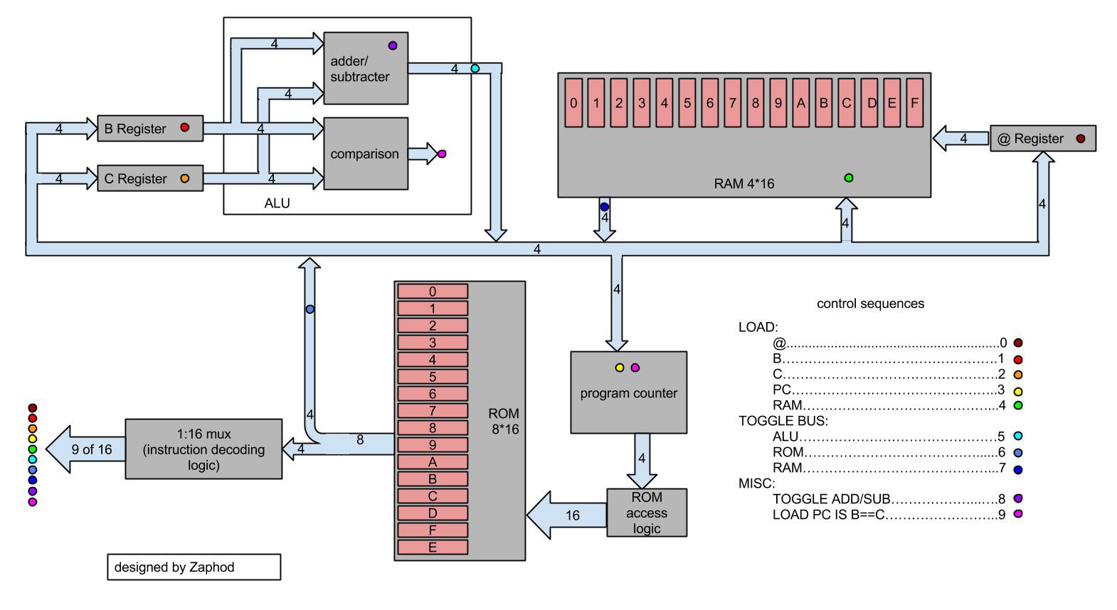
a lot of what is below is wrong. the project has gone through some major design changes, including: new architectural setup, new command set, new mechanical layout. this is the new architectural set up:

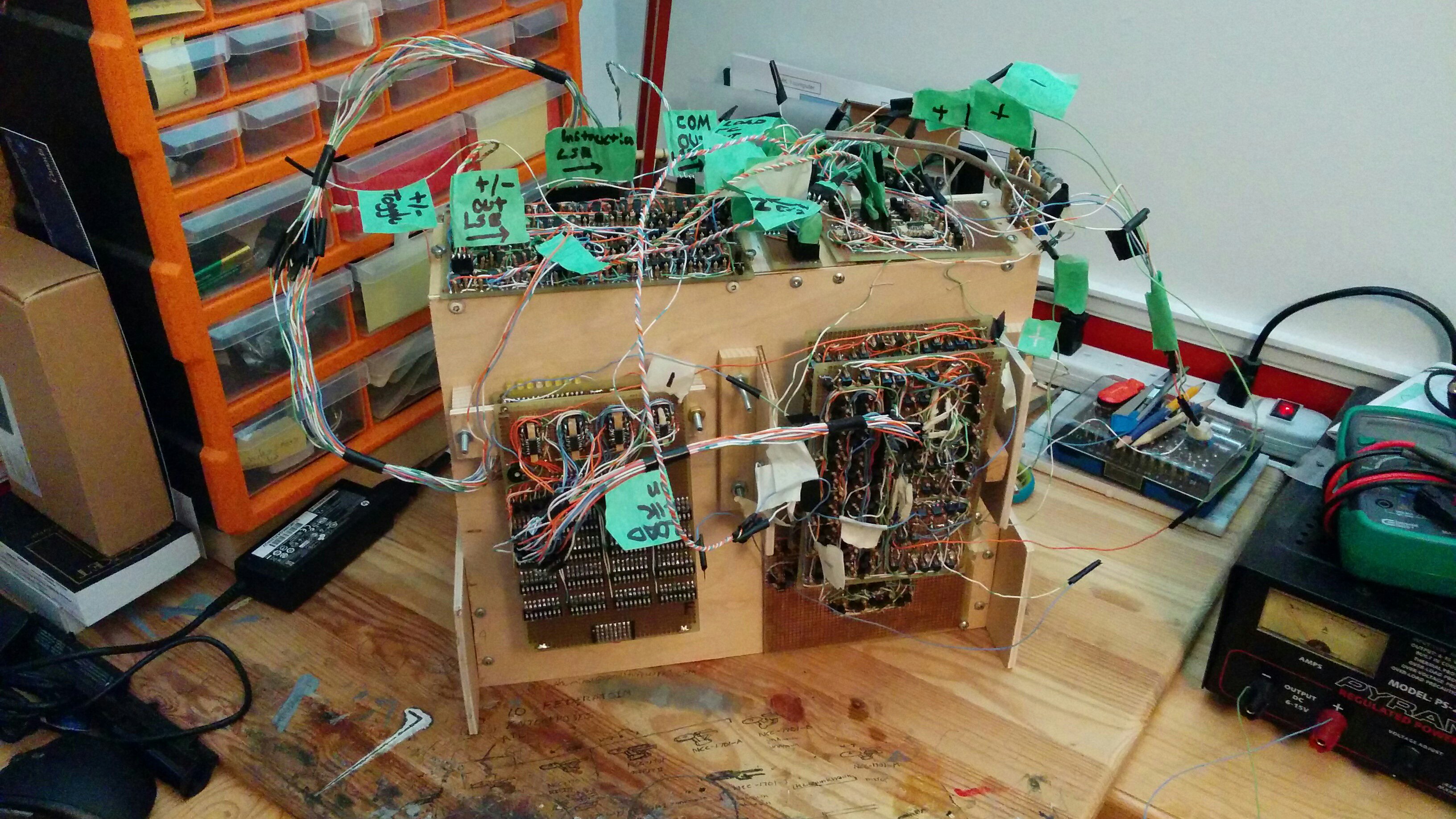
this is the new mechanical set up:
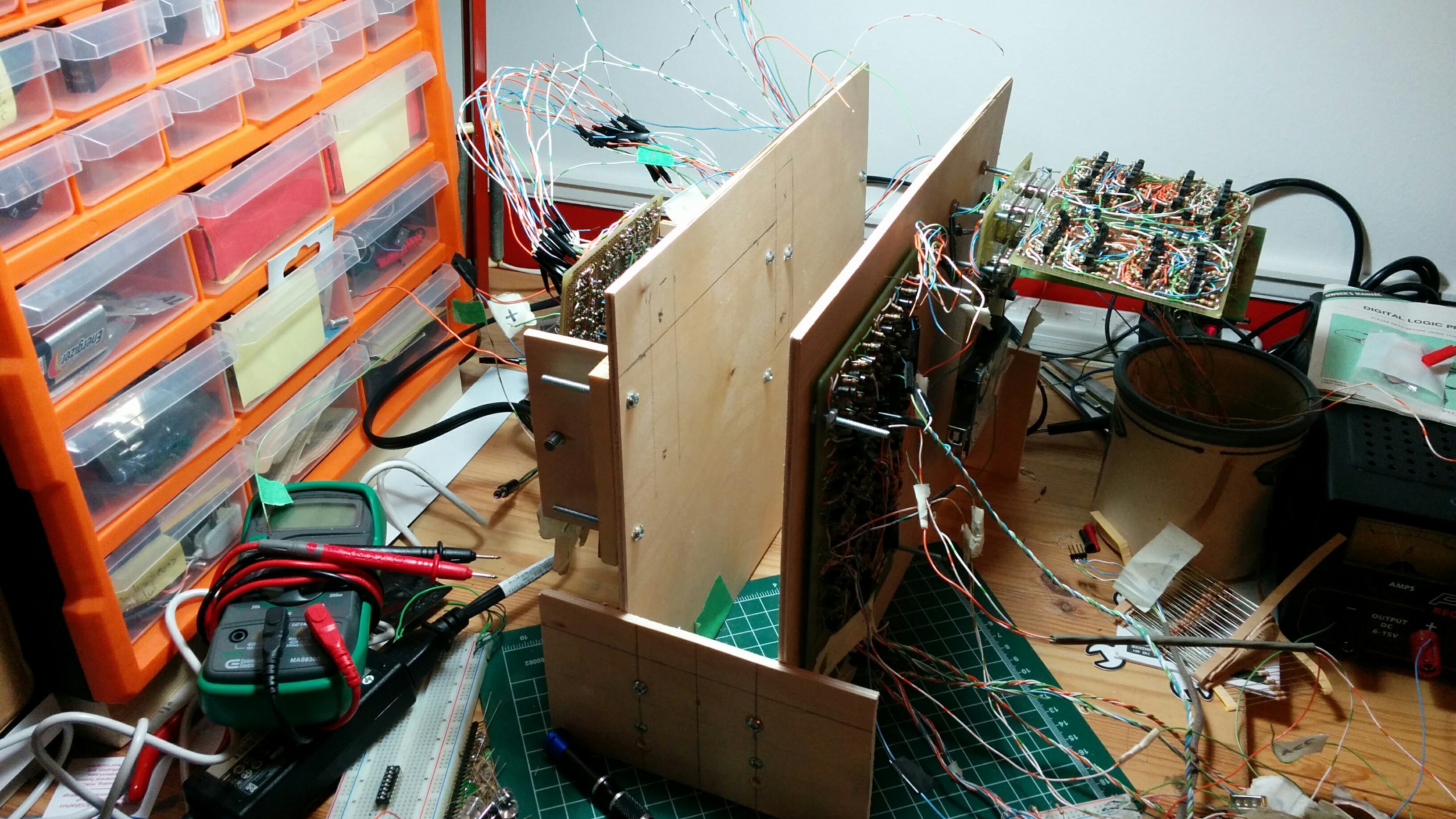
you can read about the architectural changes here.

and you can read about the command set changes in an up comping post.

I will change the below information at some point in the future.

I'm a beginner and know very little about how computers work, this is an educational project. If you find mistakes or have relevant information concerning computers feel free to comment.

The computer follows 'Harvard architecture' (I might be wrong) it has a strictly separated RAM and ROM. 4 bit is a loose indicator of bus width, the ALU is 4 bit and all the processing logic is 4 bit as is the RAM, however the ROM width ('word' length?) is 8 bits as some of the instructions contain a 4 bit value embedded.

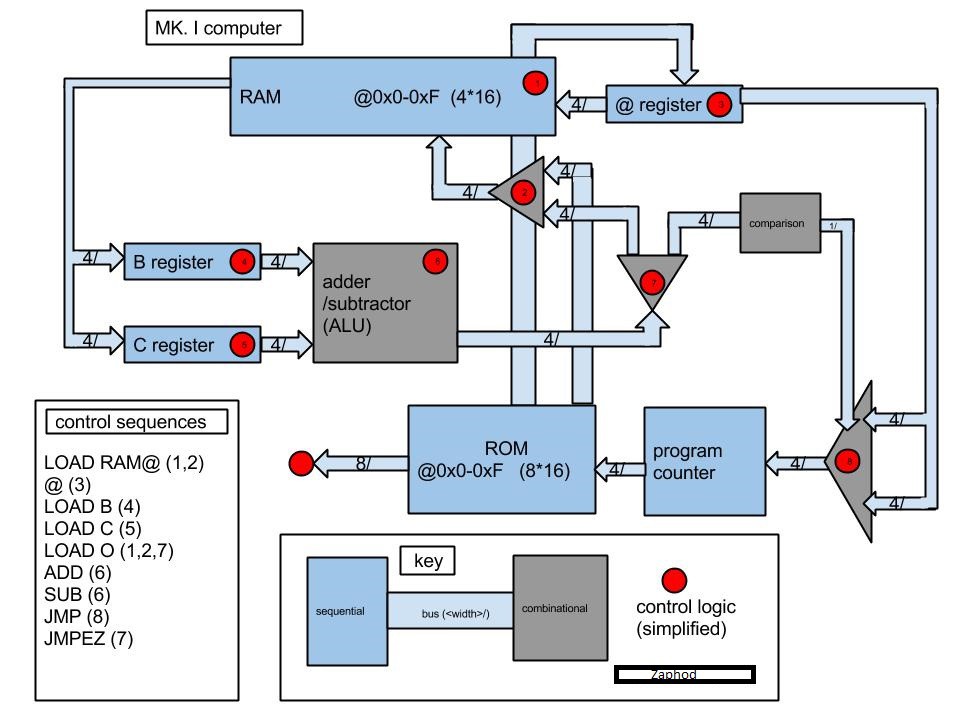
here is the architecture diagram for the computer:

major blocks:

RAM:

You might have noticed the Arduino in the (inexplicably upside down) photo. the Arduino is serving as memory, originally I had wanted the Arduino to only simulate a block of D flip flops but there are nowhere near enough pins on any microcontroller (that I know how to use) to do that, as such the Arduino also simulates some of the memory access logic. The Arduino will also serve as the only source of output, it basically just streams the contents of an array to my laptop through the serial monitor in the Arduino IDE, nothing fancy, I know, but it works. And before anyone tells me not to embed an entire Arduino board, this is by no means a finished project, I just wanted a simple way to to avoid soldering 640 transistors.

ROM:

The ROM access logic consists of a 1:16 demultiplexer with the input held high (which has been a source of quite a few problems). the memory consists of 16 dip switches and 128 diodes.
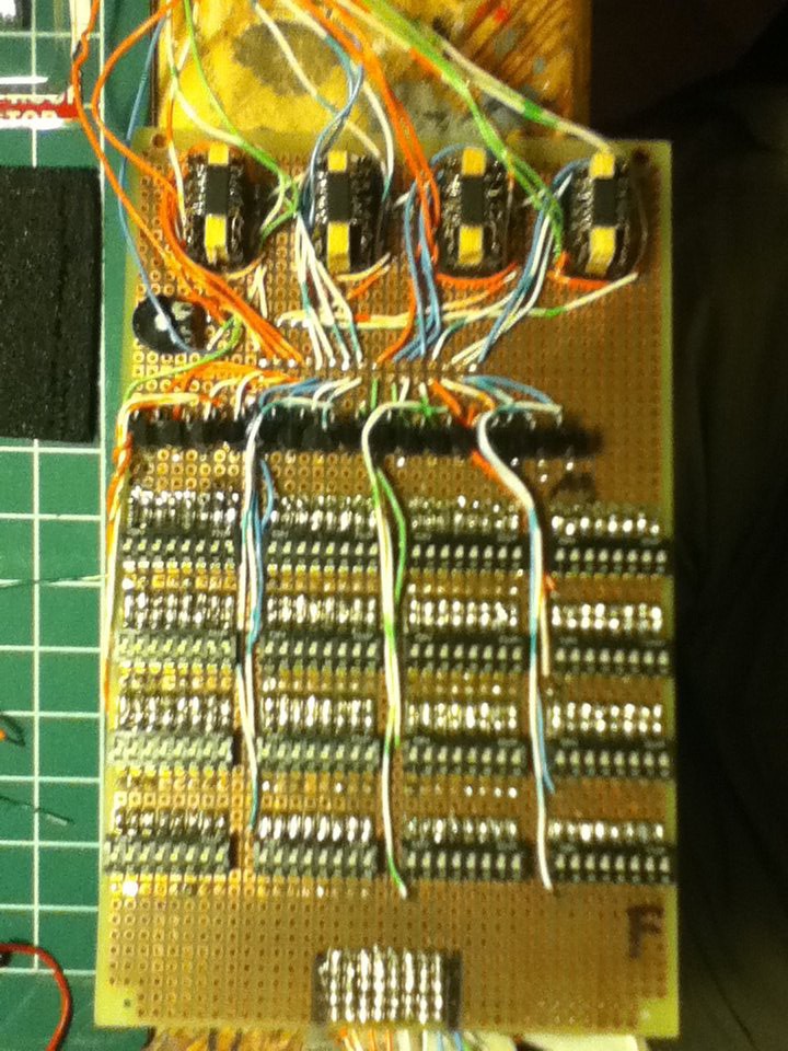
ALU:
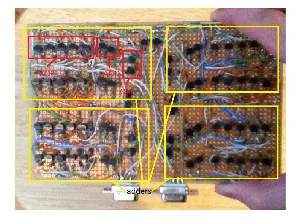
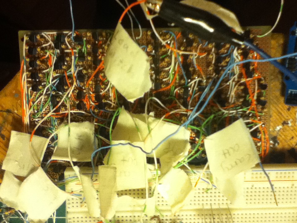
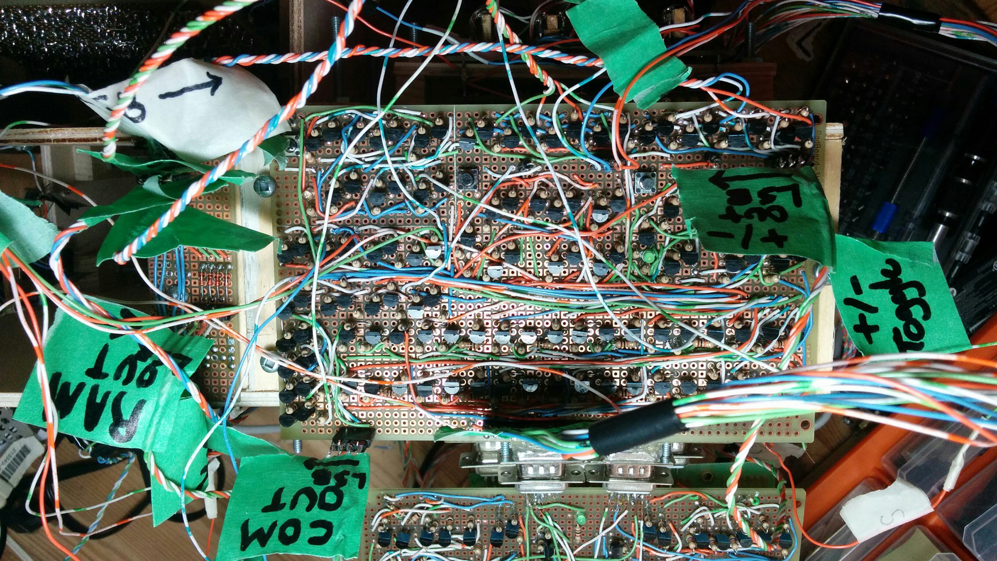
The ALU is actually just a 4 bit ripple-carry adder/subtracter. The above picture shows the 4 bit adder. To preform subtraction it uses 2s compliment math. The logic necessary to perform the invert consists of some multiplexers and inverters. The add one is done by using the extra bit on the first full adder in the adding circuitry. There is also a 'comparison unit' which will eventually be responsible for actuating the JMP (jump) command, but strictly speaking this is not part of the ALU.
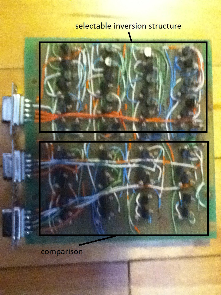
each line of transistors operates on one bit, hence four lines.

Registers:
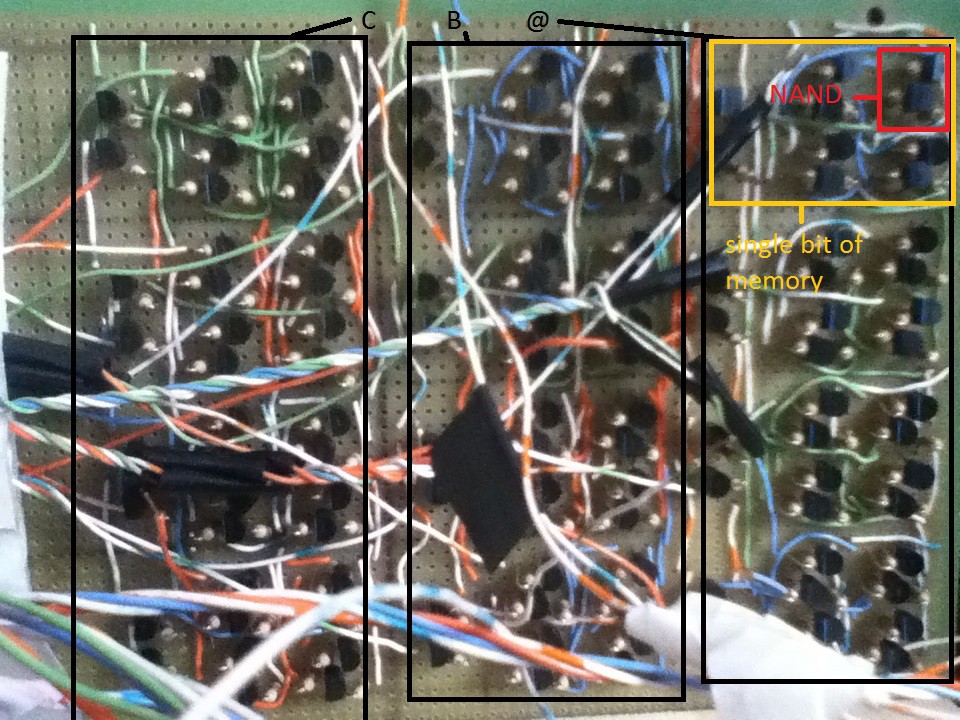
there are three registers. the first is the @ (address) register, it points to a location in the RAM with the current value to operate on. The second and third are the B and C registers, these registers are tied to the inputs of the ALU they contain the value for the ALU to operate on. While the registers could be considered memory I have decided to build these by hand. They consist of D latches built from NAND gates. Each latch requires four NAND gates, there are 12 latches total.

program counter:
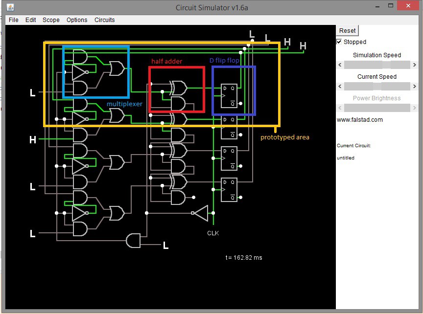
The above image was made with circuit simulator.

the above image is of the program counter in it's current state.

program counter construction details were posted in the project logs section.

The program counter's job is to count up by one in binary every clock cycle, and output the result. the output of the program counter then points to ROM address that contains the next instruction to execute. In addition to counting the program counter also has to be re-loadable by the program, I.E. the program should be able to dictate the memory location of the next instruction. Since the program can reset the program counter loops can be implemented. In addition to this if the re-loading of the program counter if done conditionally 'if' statements can be implemented.

The program counter consists of multiplexers, half adders, and D flip-flops.

these are the major blocks of the computer, there are a lot of areas I have glossed over, (control logic anyone?) but this should give you a rough idea of what...

Read more »

  • In Conclusion

    zaphod08/21/2015 at 01:37 5 comments

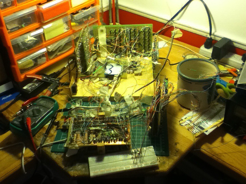
    as I mentioned in my last update the computer is finished and operational. here's a picture of its finished state:

    so what does finished mean?

    -the computer is a physical representation of the architecture diagram

    -all commands function

    -it is capable of successfully running a multi-step, multi-instruction program

    the first point is fairly straight forward as the architecture diagram omits a good deal of detail. all of the major parts of the computer seen on the architecture diagram have been present for quite some time.

    the second point is more complicated. my last post described some of the difficulty I was having with the registers and the RAM. further inspection revealed another problem: the program counter would not reload to the correct value under any circumstances. these three problems meant that 7 of the 10 machine code commands did not do what they were supposed to. the first problem was that none of the registers would accept data from the ALU or ROM, however they would load correctly if given 'good' signals. I spent a lot of time trying to clean up the logic levels with discrete components but ultimately failed. because of this I was forced to use comparators. I don't feel particularly good about using integrated circuits but I'll discuss my justifications later. the second problem was the RAM load and output enable commands not working. this problem was much easier to fix. since both the load and output enable functions are handled on the arduino each of these lines is connected directly to a pin on the microcontroller. it turns out that the logic that was generating the load signals was not producing a high that the arduino recognized, to fix this i added an amplification stage between the discrete logic and the arduino. the final problem was similarly easy to fix. the reload line on the program counter can receive data from two sources, to produce a useful output the sources must be run through an OR gate, I had been lazy and built this OR gate out of diodes, I replaced the diodes with a simple transistor OR and some amplification and the function worked properly

    the third point of my original list is the ability to run a non-trivial program. this was completed successfully on the 19th of August 2015, roughly two years after I began this project. the program I ran simply added 2 + 2 and stored the result in RAM address zero. 2 + 2 was calculated to equal 4. the program in its entirety:

    mnemonicvaluecommandcomment
    OE ROMNULL0110asserts ROM out bus to main bus
    LOAD B '2'00100001loads B register from main bus (since ROM is asserted to the main bus the value accompanying this command is also asserted to the main bus, therefore B is loaded with the value 0010 (2))
    LOAD C '2'00100010same as above except that the C register is being loaded
    LOAD @ '0'00000000same as above except that the @ (adress) register is being loaded, RAM automatically points to the address indicated by the value stored in the @ register
    OE ROMNULL0110unasserts(?) ROM out bus from the main bus
    OE ALUNULL0101asserts ALU out bus to the main bus. since the ALU is combinational in nature the values stored in the B and C registers where added instantaneously
    LOAD RAMNULL0100RAM was loaded at the address indicated by the address register.

    when the program was completed I switched the clock off and used the arduino ide to look at the contents of RAM. originally the above program produced the result 0010, however this appears to be due to the lsb and msb on the ALU bus being inverted (i put a plug in backwards) oops. after flipping the bus around the program produced the expected results.

    so that about covers it. I made a computer. the following is my reflection on the project, feel free to skip to the tl;dr at the bottom.

    was this project a success? throughout this project I have had two goals, ranked by importance they are:

    1. learn how computers work

    2. build a computer out of its constituent parts

    I feel that the first goal was achieved. I started this project with no understanding...

    Read more »

  • done

    zaphod08/19/2015 at 21:54 0 comments

    I finished the computer today and successfully ran a multi-instruction program. details will be posted soon.

  • stuff has happened

    zaphod07/22/2015 at 17:03 1 comment

    I have successfully tested and rearranged all of the modules that make up the processor and on their own each module seems to be functioning. I have also built a new board:

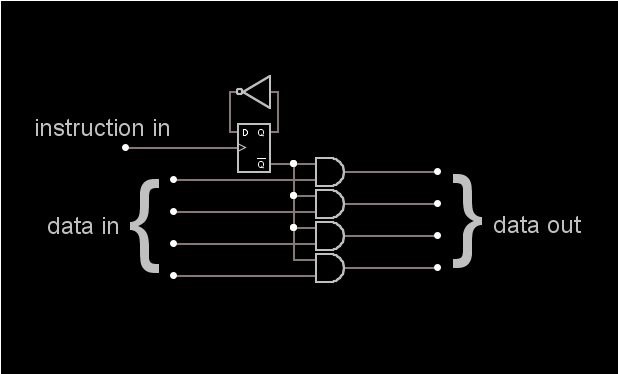
    this board is essentially just control logic it takes decoded instructions in on a 10-bit instruction bus and then turns them into usable load/output enable signals. its mostly just AND gates that AND the instruction and load clk to produce an appropriately timed load/out put enable bit. if you look at the new architecture diagram:

    you'll notice that there are only three places data on the main bus can come from: RAM OUT, ALU OUT, and ROM OUT. to decide which location data is coming from the computer needs output enables, i.e. if you want to load the @ register with a value from ROM the ROM OUT bus must be enabled and the ALU OUT and RAM OUT buses must be disabled. to do this i built a 'bus toggle' circuit:

    basically whenever the the above logic receives a 'toggle' command it switches to the opposite of what it was previously, i.e. data is being passed through>toggle>data is not being passed through or vice versa. this allows the programmer to decide where the data on the main bus is coming from by means of toggling the appropriate sources. a side effect of this is that a careless programmer can accidentally superimpose data from two sources onto the main bus at the same time. I actually only built two of the above circuit, one for ROM OUT and one for ALU OUT, the third I implemented in software on the arduino. while this is technically cheating, I don't feel it takes away from the project because, a) i have demonstrated that I can build the required circuit, and b) it is not technically part of the processor, as it is RAM access logic.

    after building the control logic board I proceeded to assemble the computer and attempt to run the very first program, it failed.

    as you would expect I was thoroughly disappointed that the computer did not work, I wasn't realy expecting to work on the first try, but still... any way I spent a lot of time retesting all of the modules in various configurations and discovered a few things:

    1. each module works as expected if it receives 'good' signals (i.e. data one = v+ and data zero = v-)

    2. the ALU works as expected

    3. the program counter ROM and ROM access logic all work together as intended, including loops, if they receive 'good' signals

    4. the register work if given 'good' signals

    5. the RAM works if given 'good' signals

    6. when all the pieces are assembled things stop working

    this was pretty mystifying. each piece of the processor seems to work on its own but when I put them all together they seize up and stop working, the RAM refuses to load, the register store data incorrectly, and the program counter resets incorrectly. at present the best explanation I have for this behaviour is that data sources (ROM, ALU, (maybe RAM)) are not giving 'good' signals. the problem with this is that I don't really know what constitutes a 'good' signal. this is because I don't know what the logic levels are/should be for RTL. because of this I only know what 'perfect' signals are i.e. connect inputs directly to positive or directly to negative. when I measure the logic levels of the data on the main bus I can see that it is not perfect, (i.e HIGH != 5v and LOW != 0v) however I don't know how to fix this using transistors. if anyone has any ideas feel free to comment.

    this problem is really bugging me because obviously some one figured out how to solve it because digital logic works, but how that was done I don't know. so far I've come up with two potential solutions for restoring logic levels to 'perfect' levels

    1. relays. relays are switches so I could theoretically use them to switch rail voltages directly. the problem with relays is that they take lots of power to switch and I'm not sure if the fuzzy values coming out of my logic would be able to flip them

    2. comparators. I've already used comparators on the project, but it was technically not...

    Read more »

  • getting there

    zaphod06/23/2015 at 23:42 0 comments

    now that exams are over I've had some time to work on the computer. as mentioned in the last couple of posts the computer's architecture has changed quite drastically, because of this most of the I've been doing has been rewiring/reconnecting modules that are already built. when this is done and all of the modules are working satisfactorily I plan to start building a little more logic, so stay tuned.

  • command set architecture and mechanical layout

    zaphod04/23/2015 at 20:49 0 comments

    as I mentioned in my last project log I have changed the command set. I won't bother reproducing the old command set here, however this is the new command set:

    mnemonicbinary (decimal)description
    LOAD:
    following commands load the indicated unit with the value asserted to the main bus
    @0000 (0)
    B0001 (1)
    C0010 (2)
    PC0011 (3)
    RAM0100 (4)loads address pointed to by @ register
    TOGGLE BUS:following commands enable/disable the indicated unit's output bus
    ALU0101 (5)
    ROM0110 (6)
    RAM0111 (7)asserts value located in address indicated by @ register
    MISC:miscellaneous commands
    TOGGLE ADD/SUB1000 (8)toggles the ALU between addition and subtraction
    LOAD PC IF B==C1001 (9)loads the PC with the value asserted to the main bus if the values in registers B and C are equal

    as mentioned in previous posts the clock is split up into two cycles, a PC CLK and a LOAD CLK. a full clock cycle would go something like this:

    rising edge of PC CLK:

    new command/value is asserted to the ROM out bus

    rising edge of LOAD CLK:

    command is carried out

    there are two major types of command, LOAD and TOGGLE BUS.

    LOAD:

    the load pin selected by the command is toggled high for the entire LOAD CLK

    TOGGLE BUS:

    the write enable for the bus indicated by the command is toggled on the rising edge of LOAD CLK. if a write enablle was already high, it would be toggled low, if it was already low it would be toggled high.

    example:

    if we wanted to write the out put of the ALU to RAM first the command TOGGLE BUS ALU would be executed, this command would would write the output of the ALU to the main bus. then the PC would increment loading the next command; LOAD RAM. this command would toggle the load pin on the RAM high for the entire LOAD CLK.

    a side effect of this new command set architecture is that values from ROM will be available one clock cycle after the TOGGLE BUS ROM command. for example to get a value from ROM to RAM one would first have to execute a TOGGLE BUS ROM command opening the ROM BUS, the next instruction would contain the value to be loaded to RAM, as the value and instruction are contained in the same ROM memory address.

    mechanical layout:

    as you may have noticed the mechanical layout has changed, this is to cope with the increase in the number of boards required for the computer. all nine logic boards are mounted on a plywood frame that is about the size of a briefcase.

  • revision time

    zaphod04/16/2015 at 02:41 0 comments

    last post I mentioned some problems. I seem to have them under control (read as: successfully swept under the rug) if you're interested in what was going on there's an explanation in the comments on the last post.

    now for the big news.

    for a while I have had a feeling that this thing was not designed as well as it could be. those of you familiar with processor layout probably noted some of the odd design choices that can be observed in the architecture diagram. notably the ALU is sort of smeared all over the place and there is not a main data bus. this leads to some weird behaviour such as an inability to load the @ register from RAM, another problem the architecture creates is a relatively ineffective conditional branching mechanism. for a while I figured I would just finish this project and build the next one right. no longer. I have decided to rework the computer's architecture. this will have a few advantages, first it will make the computer simpler, and second it will make the computer more universal. this move also comes with some setbacks, namely I'll have to take apart some of the stuff I've all ready built. fortunately all of the major logical blocks remain the same, most of the work should be in pulling them apart, not in actually rebuilding anything. all of the boards I've built will be used (except some multiplexers), but the will be connected in a new way.

    here's the old architecture diagram:

    and here's the new architecture diagram:

    what's new?

    as you can see the new design is organized around a central bus removing the need for multiplexers everywhere. an indirect effect of the bus centered design is that the control logic is simpler. you'll notice that the first diagram says that the control logic is simplified, that was my way of saying I had no idea what I was doing (as opposed to now when I have almost no idea what I'm doing). the new diagram shows control logic that is basically one level above individual gates. the complexity of the control logic is the major reason for the redesign. for the old architecture to work I would have needed to design specific control logic for each command, now I need to design 3 sets of control logic and then implement it a few times. a side effect of the revised control logic is that there is also a revised command set, one that is hopefully more universal. later this week I will post a more in depth look at the commands, what they do ,and how they work, but this is it for now.

  • update

    zaphod04/05/2015 at 02:10 2 comments

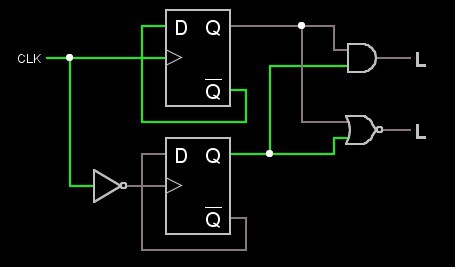
    in the last post I said I had fixed the timing problems. on closer observation I realized I had only made them slightly less noticeable. the idea of breaking up the clock is correct and the logic I proposed almost worked, but not in all test cases it turns out. I then spent some time designing slightly more well thought out logic and produced this:

    the above logic would appear to do everything I want it to. when I connected it to the program counter everything went fine, but upon inspection of the output of the instruction decoder I realized that something is seriously wrong. the instruction decoder, which had appeared to be working now does not and I don't know why. as you may have noticed this project has been on the back burner for a while, mostly due to the timing problems, but I'm going to try and figure out what's going on with the instruction decoder. as of right now I'm pretty stuck. any advice would be appreciated.

  • timing problems fixed!

    zaphod02/22/2015 at 17:40 1 comment

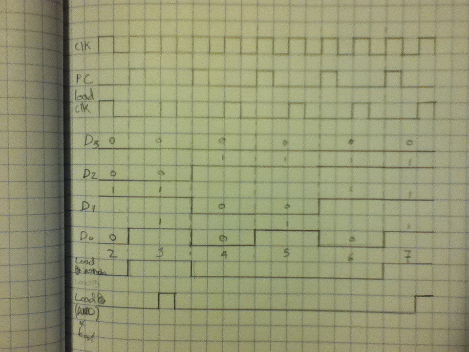
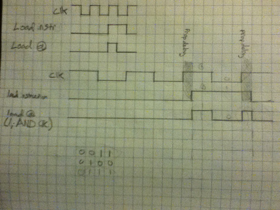
    I changed the timing of the computer. rather than trying to execute an instruction on every clock cycle, I broke up the clk into two parts. a program counter clock and a load clock. diagram:

    as you can see the program counter is incremented every other clock cycle. in stead of ANDing the clk and CMD (load @ instruction above) to produce the load @ signal I am now ANDing the load clk and CMD lines. another way of looking at it is that instead of trying to increment the program counter and write data in one clock cycle I am now incrementing the program counter in one clock cycle and writing data in the next clock cycle. the necessary logic is pretty trivial, basically a d flip flop and some gates, but the result is a working command! yay! also I'm pretty sure that since the above solution worked the double blip hypothesis was correct.

  • Timing Problems

    zaphod02/16/2015 at 18:25 1 comment

    I had always kind of assumed that it would be simplest to have the computer execute one instruction per clock cycle. it turns out this isn't the case. while my 1 instruction per clock, logic was correct I did not account for propagation delay.

    here's a quick recap of how the computer's sequential logic fits together:

    essentially the number coming out of the program counter is an address and is passed through the ROM access logic and selects and address (pink boxes). each address contains 8 bits of info (upper four are a value, lower four are a command). the value held in the ROM address indicated by the program counter is dumped onto the 8 bit bus. the upper half of the bus goes to the rest of the computer to do what ever the command tells it to. the lower half (the command) is sent through the instruction decoding logic, which is essentially a giant multiplexer (I.e 0110 (6 in decimal) goes in and 0000000001000000 comes out).

    now if I wanted to load the upper half of the 8 bit ROM bus (V from now on), into the @ register I would need to pulse the load pin on the @ register. to do this I would program a value into the lower four bits of ROM (CMD from now on) that corresponded with the multiplexer output wire that was connected to the @ register load pin. I.e. if the 12th line coming out of the instruction decoding logic was connected to the @ register load pin I would set CMD equal to 1100. that way whenever CMD==12 the @ register is loaded with the value V.

    there is a slight problem with the above explanation. V is asserted to the @ register input bus at the same time that CMD is fed into the instruction decoding logic, namely the rising edge of the clock. both values remain the same until the next rising clock, at which point they are replaced with the contents of the next ROM address. another thing to note: the @ register accepts a new value on the falling edge of the @ register load pulse. maybe you can see the problem. V and CMD change at exactly the same time. that means that the falling edge of CMD (the point at which the @ register loads) is the same point at which the value we are trying to load (V) changes, resulting iin garbage being loaded into the @ register.

    solution? my first attempt at solving the problem was as follows. add an AND gate between the clock and the CMD lines and use the output to load the @ register. because the CMD and V values change on the rising edge of the clock but we need a falling edge to load the @ register we can use the falling edge of the clock to load the @ register. if the above paragraph made no sense fear not, here is the timing diagram:

    load instr should say 'CMD'. basically Load @ = clk AND CMD. the above is logically correct, however you should note the word 'ideal' at the top of the page. as you may have heard propagation delay is a thing. I had assumed that this processor was small and slow enough that I wouldn't have to worry about propagation delay, not so! below is the 'real' timing diagram:

    again, load instruction should be CMD. between the clock and CMD there are ~200 transitors. between clk and load @ register there are 2 transistors. there is a slight lag between the clk and CMD due to the number of transistors, compared to the AND gate between clk and CMD and load @. because of this the AND gate responds almost instantaneously and you get that little double blip on the @ register's load pin. this second blip also happens right as V is changing resulting in a garbage load of the @ register on the next clock. that stupid double blip took me two days to figure out.

    I'm pretty sure that the double blip hypothesis is correct, it lines up with my observations quite nicely, however, I have not been able to observe this on my oscilloscope, although that's probably due to it being a pretty crappy oscilloscope and me not really understanding how to use it.

    how does one solve a double blip? my best solution would be to split up the clock cycle. every other clock pulse would increment the...

    Read more »

  • First Instruction Executed!

    zaphod01/31/2015 at 22:19 2 comments

    I successfully executed an instruction for the very first time. There are still some bugs to work out, but the first program shouldn't be very far off. the first instruction I executed was a load of the @ register. basically what I did was load the binary numbers 0-15 into the upper nybble of ROM, I then connected the output to the @ register input bus, and applied the clock signal. for this demo I connected the @ register load bit to the clock. eventually this will be connected to the control logic, but before that can happen I have some timing issues to fix in regards to the output of the control logic multiplexer. It shouldn't be long before this runs it's first program.

View all 21 project logs

Enjoy this project?

Share

Discussions

Bas Groothedde wrote 03/09/2017 at 10:45 point

Amazing work, that is really impressive! 

  Are you sure? yes | no

Riccardo Paolo Bestetti wrote 06/17/2016 at 09:14 point

Hey Zaphod. Of course logic gates using BJTs cause the signal level to deteriorate as CE voltage of consequent NPN switches will be less and less each time. How do you deal with that?

  Are you sure? yes | no

Milly wrote 06/14/2016 at 15:28 point

That's so awesome ! I plan on making something like this. Can you please give the detailed list of components and circuit diagrams? Also you have designed everything using transistors, I can  use ICs instead, right ?

  Are you sure? yes | no

franz wrote 06/02/2016 at 02:11 point

Hey zaphod, what is the discreet transistor you are using ?

  Are you sure? yes | no

zaphod wrote 06/02/2016 at 02:48 point

2n3904. Nothing special.

  Are you sure? yes | no

franz wrote 06/02/2016 at 03:32 point

Thank you ! I am teaching electronics to my kids and what you did is such an inspiration, thank you for sharing it.

  Are you sure? yes | no

Ajekiigbe Damilare wrote 03/18/2016 at 22:25 point
You referred to an article "logic gates" on hyperphysics in your article, my question is "are the gates you used similar in circuitry to those one (on hyperphysics) or you add some components"?

  Are you sure? yes | no

Ajekiigbe Damilare wrote 03/18/2016 at 22:24 point
You referred to an article "logic gates" on hyperphysics in your article, my question is "are the gates you used similar in circuitry to those one (on hyperphysics) or you add some components"?

  Are you sure? yes | no

Ajekiigbe Damilare wrote 03/18/2016 at 22:23 point
You referred to an article "logic gates" on hyperphysics in your article, my question is "are the gates you used similar in circuitry to those one (on hyperphysics) or you add some components"?

  Are you sure? yes | no

Baran AKBIYIK wrote 12/31/2015 at 00:15 point

Awesome man just awesome

  Are you sure? yes | no

Jason Westervelt wrote 12/23/2015 at 01:10 point

This thing has got to be a power hog, lol

  Are you sure? yes | no

Çetin Köktürk wrote 07/19/2015 at 20:33 point

This was my dream project, it's nice to see someone actually did the research & spent effort on it.
By the way, you made a computer from scratch but you didn't know the astable multivibrator... you are an interesting man :))

  Are you sure? yes | no

Tiago Damian wrote 04/26/2015 at 20:21 point

Impressive build,.

  Are you sure? yes | no

Faruq Sandi wrote 01/07/2015 at 03:25 point

impressive!

  Are you sure? yes | no

Faruq Sandi wrote 01/07/2015 at 03:25 point

impressive!

  Are you sure? yes | no

Russell McMahon wrote 11/23/2014 at 10:11 point
!. Utterly awesome
2. You must bemad!
3. Utterly awesome :-). Keep up the good work.
Look at serial in parallel out and parallel in serial out shiftregisters as an Arduino replacer.
(Memory says eg CD4021, CD4094?)

  Are you sure? yes | no

zaphod wrote 11/23/2014 at 15:10 point
I had thought of using something other than an Arduino for the RAM, but the Arduino has the big benefit of being able to display the contents of the RAM through the serial monitor without the need for extra hardware.

  Are you sure? yes | no

EK wrote 08/18/2014 at 22:24 point
Very cool seeing this at Maker Faire Ottawa! It is quite intense!

  Are you sure? yes | no

Charles Eidsness wrote 08/18/2014 at 00:24 point
Saw your build at the Mini Maker Fair. Great job!

  Are you sure? yes | no

Hari Wiguna wrote 06/11/2014 at 13:05 point
Wow! That's a lot of transistors and wiring! Very impressive!

  Are you sure? yes | no

The Big One wrote 05/02/2014 at 01:31 point
Very cool! I've designed a CPU from the ground up in university, but was never brave enough to implement in real life. All... those... wires.... ! :-)

  Are you sure? yes | no

zaphod wrote 05/02/2014 at 22:15 point
Thanks for the comment! I don't think I'd call myself brave... maybe more like I didn't know what I was getting into.

  Are you sure? yes | no

Similar Projects

Does this project spark your interest?

Become a member to follow this project and never miss any updates