Kris Winer
-
First Assembly of ESP-PICO-D4 Development Board
03/20/2018 at 01:48 • 2 comments03/19/2018
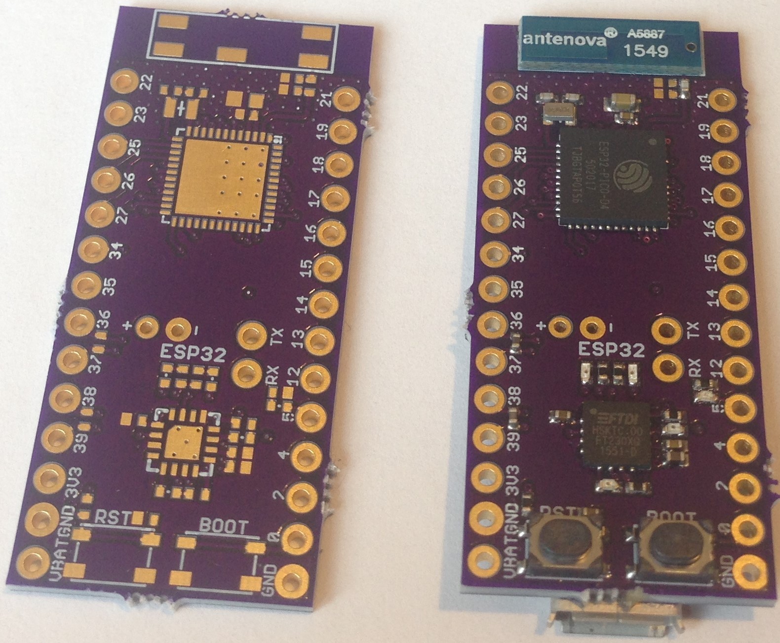
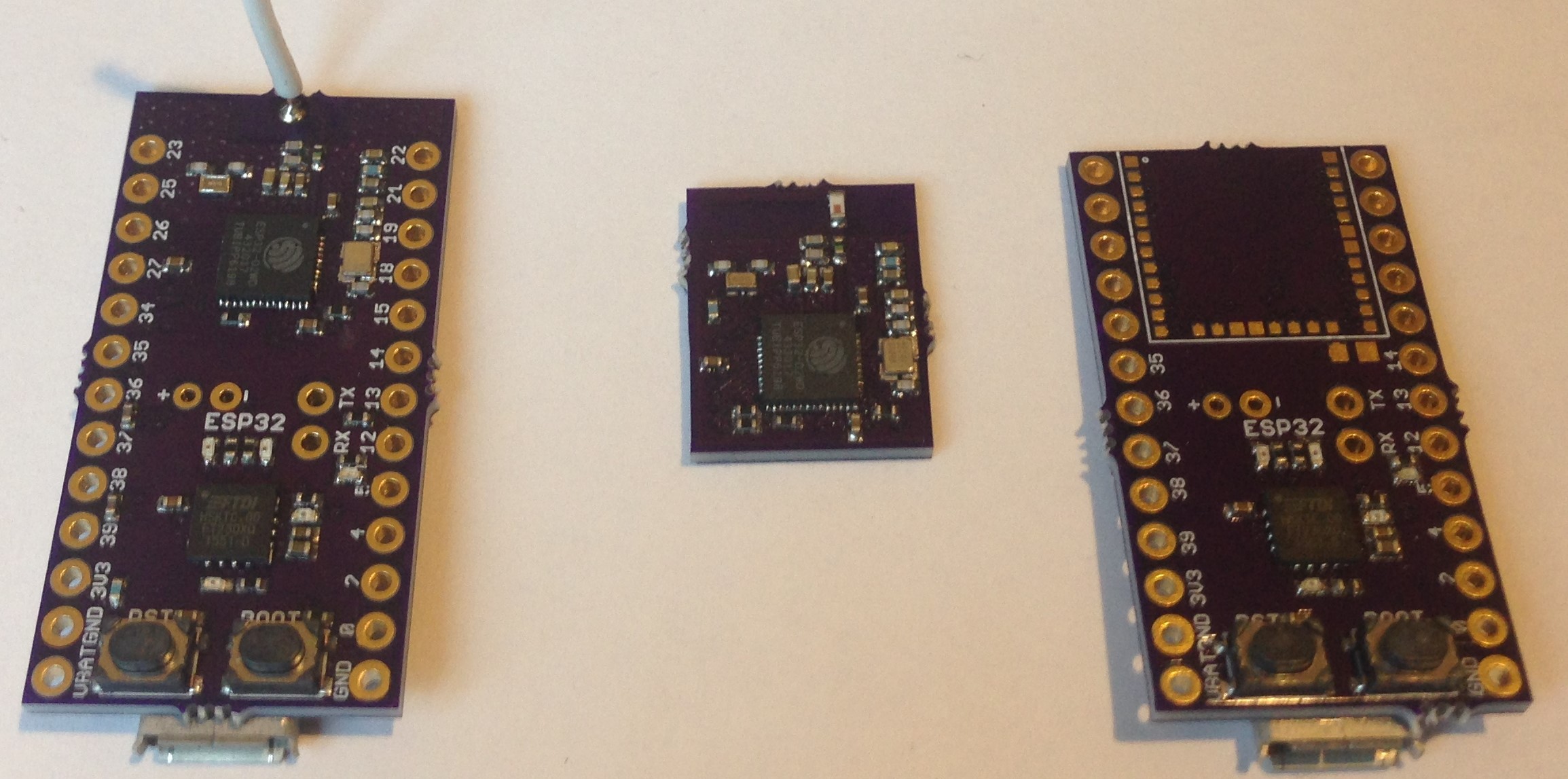
I got both the ten ESP32-PICO-D4 ICs I ordered from Electrodragon and the three pcbs I designed for them from OSH Park today. So I immediately went to work assembling the components to make my first ESP32-PICO-D4 development board.
The assembly of the LDO, battery charger, USB, FTDI chip, etc went as usual as I have done this dozens of times so nothing interesting there. The assembly of the PICO IC was super easy, no terrifying 0.35-inch pitch IC like the ESP32-D2WD. In fact, the PICO is easier to solder well than any of the ESP32 ICs I have tried. More like soldering the ESP8285/66. And with most of the components embedded in the PICO putting the entire board together took less than an hour, where usually just the ESP32 part takes this long.
The board worked first time out. I was able to flash a program using the Arduino IDE using ESP32 dev module, DIO, 80 MHz flash speed, 921600 UART speed, and 2 MByte flash selections (I got the flash size wrong but it didn't seem to matter). I got the led blinking, serial data (battery voltage and chip temperature) streaming to serial. I need to test the pin functionality, etc but so far so good!
I tested the wifi and was seeing up to four networks including my home network, an extender, a laptop and my neighbor's wifi network. The Antenova performance seemed to be about as good as the pcb antenna on the ESP32-WROOM module and slightly poorer than a monopole copper wire but it is hard to tell with RSSI alone and I would like to find some convenient way to test and optimize the antenna performance short of buying a network vector analyzer.
Here is what the board ended up looking like:
![]()
![]()
Overall I am so pleased with the performance and ease of assembly and low cost of the ESP32-PICO-D4 that I am abandoning any attempt to create a module of my own since Espressif has done such a wonderful job of it. Kudos Espressif!
-
Skunked!
03/09/2018 at 02:13 • 0 comments0308/2018
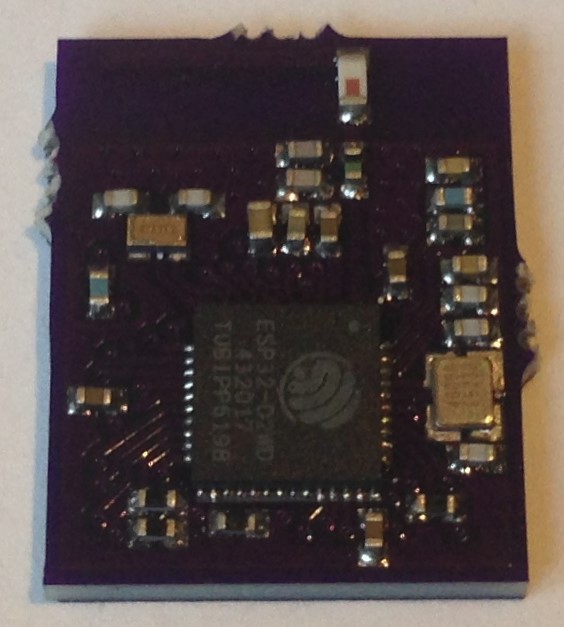
While trolling the Hackchat forum I happened to come across a mention of the ESP32-PICO-D4 which I had never heard of. Well, it turns out this is a SoC (System-on-a-Chip) like the ESP32-D2WD with 4 MBytes of embedded flash instead of the 2 MBytes of embedded flash of the D2WD. Furthermore, even though the PICO is 7 mm x 7 mm (2x larger in area than the 5 mm x 5 mm D2WD) it contains the 40 MHz crystal, and almost all of the passives required to make it work. Plus, as a QFN48 package with 0.5 mm pitch it is a whole lot easier to assemble than the D2WD, which still gives me nightmares.
So here is the easy-to-use, compact module I was trying to make already available for about $5. Not much point fooling around trying to make my own module then when Espressif has already done it and better than I ever could.
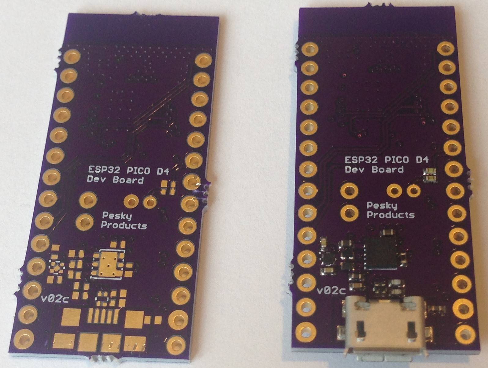
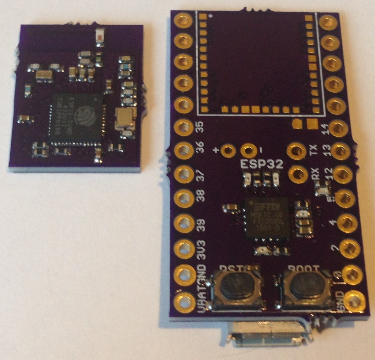
So, I bought ten of the ESP32-PICO-D4 from Electrodragon, replaced my module with the ESP32-PICO-D4 and submitted the new development board to OSH Park. I expect to get the pcbs and ICs at about the same time and have a working board by the end of March. Here is what it looks like unpopulated:
![]()
I chose to add a 32.768 kHz crystal for the RTC, but this is not required. I would have had the 0603 10 uF capacitor anyway for the board using my own module and the extra 100 nF capacitor is in the reference schematic. As is a pi matching circuit to tune the RF to optimize the coupling to the Antenova antenna. But I expect either a small capacitor or 0 Ohm jumper will be enough to connect the LNA-IN to the antenna. So really, almost no external components are really needed with the PICO solution. Sweet!
I kept the FTDI USB-to-UART connector and battery charger and buttons, etc that I use for all of my ESP32 development boards.
So this could be nearly the perfect solution for rapid customization of hardware designs using the ESP32. And I like the fact that the PICO has 2 Mbytes more flash and allows use of GPIO16/17 (since the PICO flash operates in the 3.3 V domain) unlike the D2WD IC.
I will report on the board assembly and performance in a couple of weeks. In the meantime, I am suspending development of my own module. No point now really...
-
Wifi Antenna Performance
03/04/2018 at 19:42 • 0 comments03/04/2018
I ran a simple wifi scan program as a test of the antenna performance and found the chip antenna quite disappointing. For the 1.2-inch wire antenna, I found the two wifi hotspots in my house (router and extender) at RSSI of -27 and -59 dB, on average, and about half the time I also detected the neighbor's wifi at -93 dB. With the ESP-WROOM dev board and its pcb antenna I did a little worse, finding the two in-house stations at -30 and -67 dB and once I also found the neighbors at -91 dB. Worst of the three was the chip antenna, which found both in-house hotspots at -38 and -71 dB and never saw the neighbors wifi. This is only a semi-quantitative result but it is clear that either the chip antenna is improperly designed (I guessed, after all) or the matching circuit is way off. I think this means short of a network vector analysis and pi match tuning, I am going back to the wire antenna solution...
-
First Module Assembly...Success!
03/04/2018 at 01:48 • 0 comments03/03/18
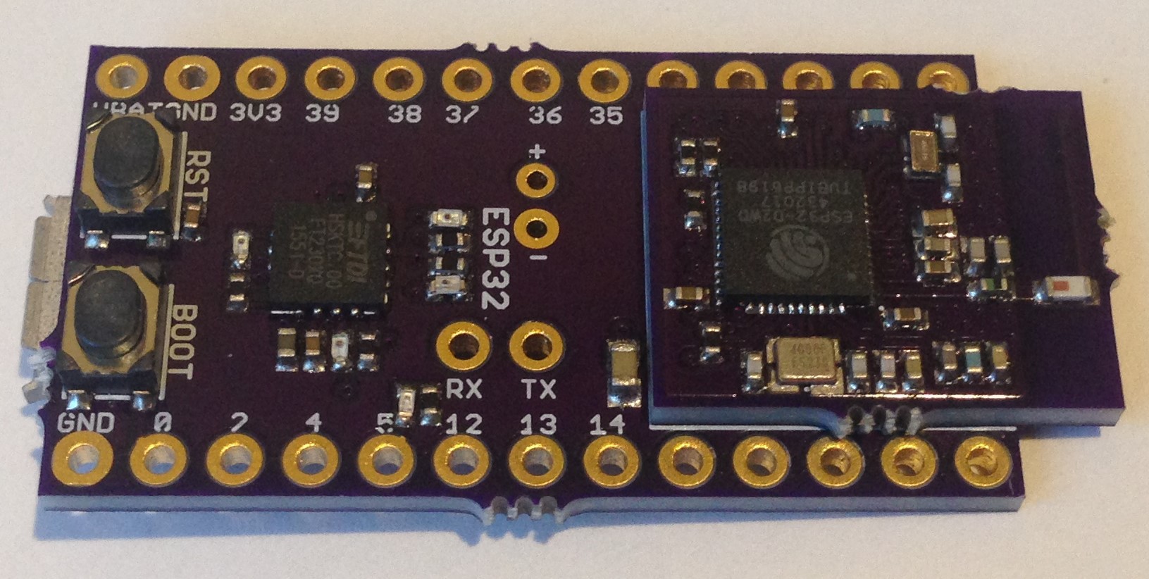
Phase 2 is assembling the module onto the acceptor board. Now this process is straightforward and I expect success in the sense that I will be able to actually solder it uneventfully. Here it is:
![]()
To my delight, I was able to flash the same blink program and get it to work the first time out. The battery voltage monitor on pin 34 seems to be reading too high, but the led blinks and I am reading the ESP32 chip temperature. Now to do some more testing in the next few days to compare the performance between the integrated board and the modular one. But overall, I declare victory!
Now if I choose to go ahead and have some modules made there are a couple of changes I would make. One is I would use an 0.8-mm-thick pcb to reduce the overall height of the module and make reflow easier. I would also insist that the module have straight edges instead of the somewhat ugly mousebite remnants that come with the OSH Park boards. I would add more ground vias to the ESP32 thermal pad to improve the heat sink and reduce the inductance between the board and IC. I would probably also add a thermal pad onto the acceptor board like the WROOM module for the same purpose.
I am not sure about the metal can. There are design houses that can make custom RF enclosures but I am not sure I want to incur the expense. Perhaps I will make one more design iteration to add the vias and thermal pad before I declare this modular design good enough. Some testing of the peripherals is in order as well while I wait for the design revision.
Somewhat to my surprise, it looks like this idea not only has merit but is cursed with working the very first time! Maybe I should quit while I am ahead...
-
First Module Assembly
03/04/2018 at 00:49 • 0 comments03/03/18
Just completed Phase 1 of the ESP32 module assembly. The strategy in a nut shell is (Phase 1) to assemble an integrated development board using the ESP32 D2WD and then a module with same, then (Phase 2) solder the module to the acceptor board and (Phase 3) compare performance of the integrated board to the modular board.
Here is the collection of boards at the end of Phase 1:
![]()
Initial assembly of the two ESP32 ICs and surrounding circuit was reasonably quick but it took me a long time to cure the last of the solder bridges. This 0.35-mm-pitch is tough!
I verified I could flash a blink program (ESP32 Dev Module, QIO, 80 MHz flash speed, 2 MByte flash, 921600 upload speed) onto the integrated board using the Arduino IDE and the led works and I am getting battery voltage and ESP32 IC temperature on the serial monitor as requested. So at least the basic design seems sound and the integrated board works.
I soldered a 1.2-inch copper antenna on the integrated board, which provides adequate reception. One of the things I want to test is the reception of the chip antenna relative to this monopole wire antenna solution.
Here is a close up of the module before I assemble it onto the mother/acceptor board:
![]()
Everything except the ESP32 D2WD itself is easy to assemble. I am using the 40 MHz HSE crystal in this design even though I had used the same 26 MHz crystal in my original ESP32 and ESP8285 development boards. The ESP32 works with the 26 MHz crystal but since the current version of the ESP32 reference design uses 40 MHz so will I.
Next task is to solder the module onto the acceptor board:
![]()
Next, Phase 2...
Small ESP32 Module for Easier Custom Design
Unhappy with the ESP32-WROOM module, I designed an ESP32 D2WD module to ease custom board assembly and enable small, wearable ESP32 devices