-
Spike Impulses and Three State Memristors
12/05/2015 at 19:04 • 0 commentsI've come across two research papers that have caused me to rethink my previous designs. The first outlines using a single memristor to perform all logic operations via spike operations. The second outlines how a memristor with two detectable hysteresis curve can be used to store more than two values.
The paper outlining single memristor logic carries a lot of weight for me. Using the short-term memory effect of the memristor, and several other neurological processes that have been adapted electronically (blocking out noise stimuli, for example), input registered as voltage spikes will have a corresponding current spike. Like implication logic, these spike impulses work by performing a basic memristive operation to whichever state is present in the memristor's short term memory. The paper also covers reversible logic operations within one memristor, which would add another feature to this architecture. This is all well and good, but the paper is riddled with grammatical and spelling errors. Additionally, some figures are not properly captioned, casting confusion over the entire spike impulse process. Regardless, I feel that this may be an easy way to greatly simplify my prior designs. One needed feature will be converting the resulting current spikes into voltage spikes, and additionally storing this data as a different resistive state for the long term.
A second IV curve may be accessed via higher voltage and a slower sweep, as shown by the second research paper. This second state occurs with an inverted IV curve relative to the first IV curve. In addition to being proofread, this paper gives explanations as to the electrochemical interactions taking place inside of the memristor.
I am going to occupy my time with familiarizing myself with the content of these papers and trying to apply their techniques to this project. At the very least, I'll have my previous implication logic system if this ends up being a dead end.
-
IMPLY Voltage Controller
10/05/2015 at 04:19 • 0 commentsHere's a peak at something I've been playing around with:
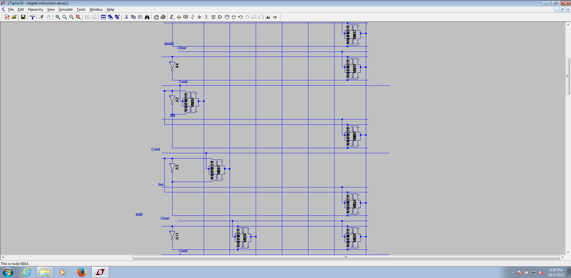
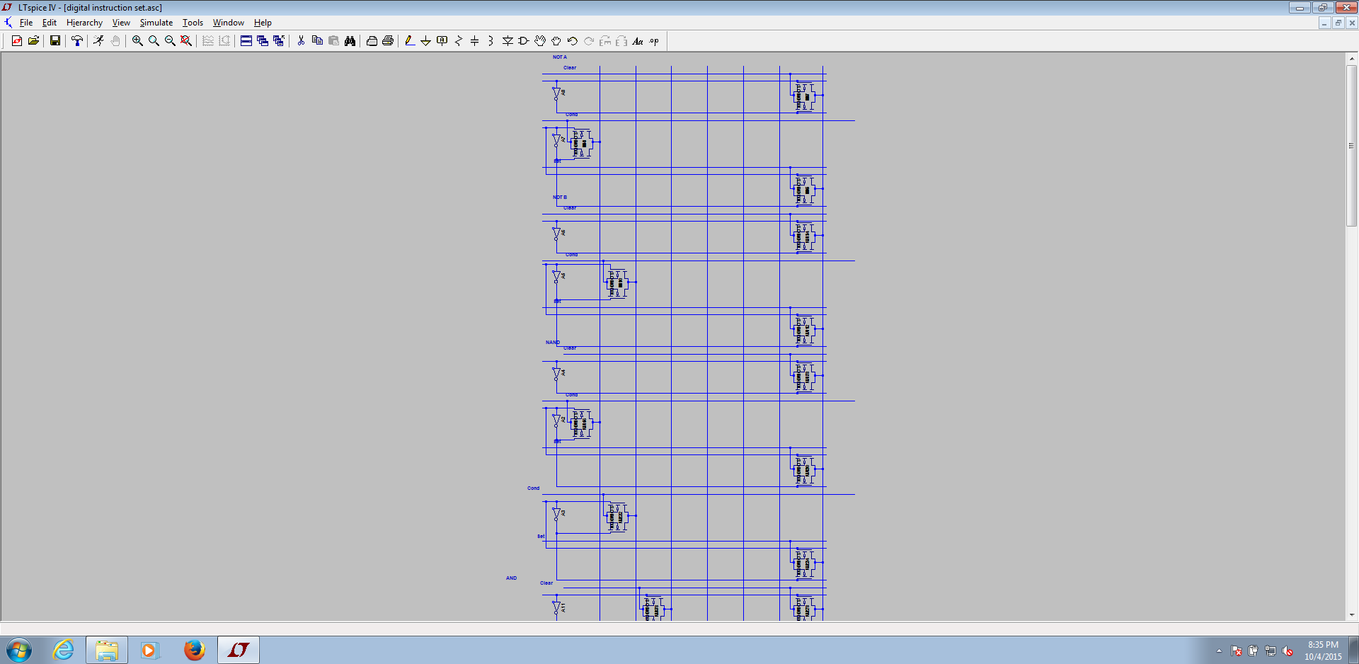
 This circuit can be used to perform imply based logic functions. I've been implementing the previously posted digital instruction set. If anyone wants the exact spice file I'm using, message me. Each pair of transmission gates sends the corresponding Condition and Set signals required to perform imply operations. By moving downward sequentially, the correctly timed signals manipuate the memristor crossbar array connected to the vertical wires. This operation can be compared to the rotating barrel in a music box striking the correct notes at the correct time when directional force is appled. Different logic functions are grouped into sections.
 There are two ways I'm thinking of to trigger each row. One way would be to have a clock increment a binary decoder for the corresponding instruction, moving execution line to execution line with each clock cycle. Another method would be to have a decoder trigger the first execution line in an instruction, then have a delay buffer inbetween each execution line move through the steps automatically until the last step is completed. The first execution signal and the last, delayed execution signal could be used to switch a basic latch to indicate whether the memristor controller is busy or ready. This would facilitate asynchronous operation in a system.
My starting point for the design of this controller was diode based ROM. Each addressed row of diodes provides the correct data output. If someone were to intergrate an EEPROM into a full grid of transmission gates, different logic functions could be microcoded. This opens up interesting possibilites for programmable logic.
Being that this memristor controller can store and process data, a basic CPU of sorts could be made with an X by X sized grid of these controllers. This grid of memristor controller units would have a 1:1 ratio of processing power to storage, FPGA technology could be used to route signals from one controller to another. Additionally, if each controller shares their vertical wires with a common bus, mass instruction propagation may be performed. This can be used to perform content addressable memory operations (compare word-length blocks of controllers with search key using an equality function).
I have come up with a timing set for ternary operations, but I'm not going to manually enter it into a grid in a blogposting. At the moment, it resides in an excel file. Message me if you're interested in seeing this. If anyone has any suggestions for secure and free filesharing solutions please let me know.
While I have put a lot of effort into material implication based memristor designs, there are other, possibly more efficient methods of processing with memristors. I plan on investigating as many of these methods as I can. This paper in particular covers many different memristor processing methods.
-
Well needed update
09/22/2015 at 15:53 • 0 commentsIt's been a while since I've had anything to say. There are a couple of good reasons for this, but more on that later.
First, I'd like to make some observations on memristor technology in general. I took a very long break from working with memristors because most of the research is either blocked by an academic paywall or going straight into military applications.
As you can see in the profile picture for this project, I tried my hand at memristor fabrication on my own. Following the advice of the nice guys in the beam robotics mailing list, I oxidized copper and connected it with an aluminum foil terminal. All of the devices show worked for about a week, until I burnt them out. One interesting effect that observed was that each memristor device would oscillate at a descending frequency when attached to an amplifier. Aside from demonstrating the memristor effect, these devices were useless. Every professionally made memristor that I've seen (I am no expert, I am probably incorrect with this information) doesn't have a solid reliability rate. Several papers have asserted that the true memristor has not been found yet, and may be physically impossible. I'm not sure about impossible, but I can't imagine this technology diffusing into the public sector until several improvements are made to the memristor fabrication process. This hampers my own research, as I can only make designs on paper and simulations in LTspice. I'm confident that the field will expand and mature, much as transistors did in the early 60s.
Finally, I realize that I've yet to make any substantial publicaitons of my own designs. This has been partially because of my busy schedule in college, but mostly out of sheer laziness. Additionally, I can never find a satisfactory settling point for my own work. I published the digital timing set mainly because my own design is based around ternary logic. More recently, I've been researching reversible computing and see a lot of potential for it to mesh with my own work. In this week I will publish an overview paper of my work.
Until next time!
-
Digital Logic Functions
08/26/2015 at 21:06 • 0 commentsGreetings!
Here I have attached a table of condition and set voltages that may be stepped through to perform digital logic operations on a crossbar array. I have checked the results by hand, but have been unable to replicate them in spice (due to a lack of knowledge with ltspice and model creation...) or in real life. Please contact me if you have any applications for my work that are fruitful.
Logic operation Comments A B W0 W1 W2 W3 Q Invert (A/B) Clear Registers Clear IMPLY (A/B) to Q Condition Set NAND Clear Registers Clear IMPLY A to Q Condition Set IMPLY B to Q Condition Set AND Clear Registers Clear Clear NAND A and B to W0 Condition Set Condition Set IMPLY W0 to Q Condition Set OR Clear Registers Clear Clear Clear IMPLY A to W0 Condition Set IMPLY B to W1 Condition Set NAND W0 and W1 to Q Condition Set Condition Set NOR Clear Registers Clear Clear Clear Clear IMPLY A to W0 Condition Set IMPLY B to W1 Condition Set NAND W0 and W1 to W2 Condition Set Condition Set IMPLY W2 to Q Condition Set XOR Clear Clear Clear Clear Clear NAND A and B to W0 Condition Set Condition Set NAND A and W0 to W1 Conditiont Set Condition set NAND B and W0 to W2 Condition Set Condition Set NAND W1 and W2 to Q Condition Set Condition Set XNOR Clear Registers Clear Clear Clear Clear NAND A and B to W0 Condition Set Condition Set NAND A and W0 to W1 Condition Set Condition Set NAND B and W0 to W2 Condition Set Condition Set NAND W1 and W2 to W3 Condition Set Condition Set IMPLY W3 to Q Condition Set

