Andrew Starr
-
Simulator
08/25/2016 at 07:47 • 0 commentsI have written an instruction set simulator for the T-1. It is an arduino sketch, and runs on an Arduino Mega 2560, using the onboard UART to provide the operator interface. Current simulator functionality includes:
- Single step and continuous execution modes
- Execution breakpoints
- Inspect and modify stacks, system RAM and code memory
- Inspect and modify top-of-stack register and program counter
- Halt on stack under- and overflow
To get a program into the simulator, I have written a shell script that does the following:
- Calls the ASL assembler to assemble the code
- Calls P2HEX to convert the assembled code into an ASCII hex format
- Converts the hex file (using awk) to a header file that is an initialised C array of unsigned ints
When the sketch is uploaded to the arduino, the header file is included and provides the instructions for the simulator.
The simulator will allow me to experiment with different instructions, and allow me to test programs before I commit to wiring them.
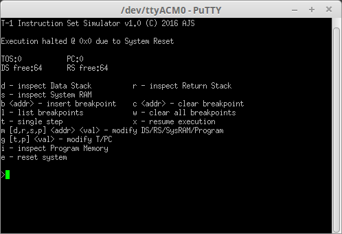
Here's a screen capture of the main menu:
![]()
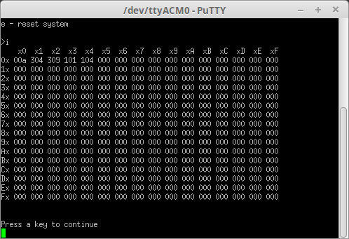
and a code memory dump:
![]()
-
Assembler
08/12/2016 at 23:11 • 0 commentsI now have a functional assembler for writing T-1 code (in order to generate wiring patterns It supports macros, which will help a lot, given my restricted instruction set. It is based on the AS macroassembler by Alfred Arnold. It is a crossassembler that supports many processor families. Arnold includes straightforward instructions in the manual for adding new processors, which I have followed to add T-1 support. Here's an extract of the list output for some simple looping code:
       1/       0 :         cpu t1
       2/       0 :
       3/       0 : =0xA    counter	equ	10
       4/       0 :
       5/       0 : 000A                push	counter
       6/       1 : 0304    loop1:	dec
       7/       2 : 0309                skz
       8/       3 : 0101                jump	loop1
       9/       4 :         loop2:
      10/       4 : 0104                jump	loop2
      11/       5 :
I am currently working on an instruction set simulator, which will run an on arduino mega 2650 board (the same board I use to test logic modules after I make them). The arduino will take the assembler output and simulate execution, allowing me to test the program functionality, inspect stack and memory contents etc - before I commit to handwiring a ROM board!
-
Now with sub-projects!
04/20/2016 at 09:17 • 1 commentThe T-1 project blog is beginning to get a bit unwieldy, so I have decided to document the computer sub-systems as separate projects, and use this one as a 'top level' project to tie everything together.
The ferrite core memory is the first sub-project, it will be followed (eventually) by the ALU, program memory, etc. as I work through and build them.
-
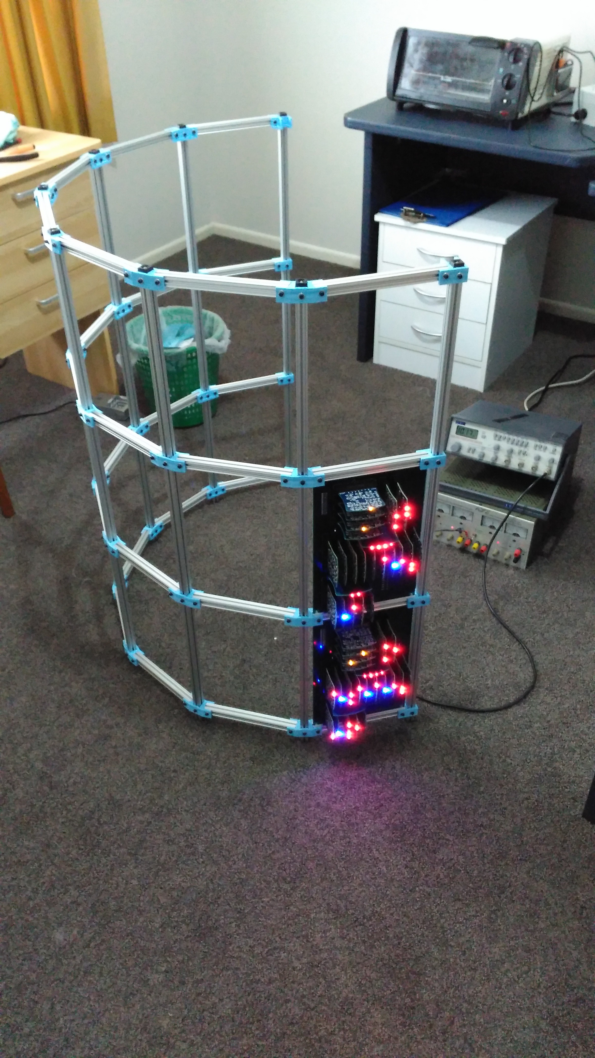
Core Blimey Part II
04/19/2016 at 08:17 • 7 commentsI had a false start with the first prototype core array, where I discovered that my core orientations and sense wire threading pattern were picking up noise from half-selected cores, causing the sense amp to register non-existent core transitions. I've redone the array wiring in such a way that the orientation of the cores and the path of the sense wire through them results in the half-selection signals cancelling out.
Here's a photo of a 'new pattern' array:
![]()
To date I have wired 8 core arrays, so I have enough for 1 complete 64-byte memory module.
I've also prototyped a core selection module. This module will take as inputs an active low signal (one of the row/column selection bits), and a control bit (which will determine what the polarity that the selected drive line is driven in). It is effectively a modified dual 2-input NOR gate. The inputs are common to both gates, and one gate has a PNP transistor where the other has an NPN, so they will respond to opposite polarities of the control bit. The 2 gate outputs go to the 2 drive inputs of the H-bridge controlling a particular row or column drive line. There is a selection circuit and H-bridge for each of the 16 drive lines.
![]()
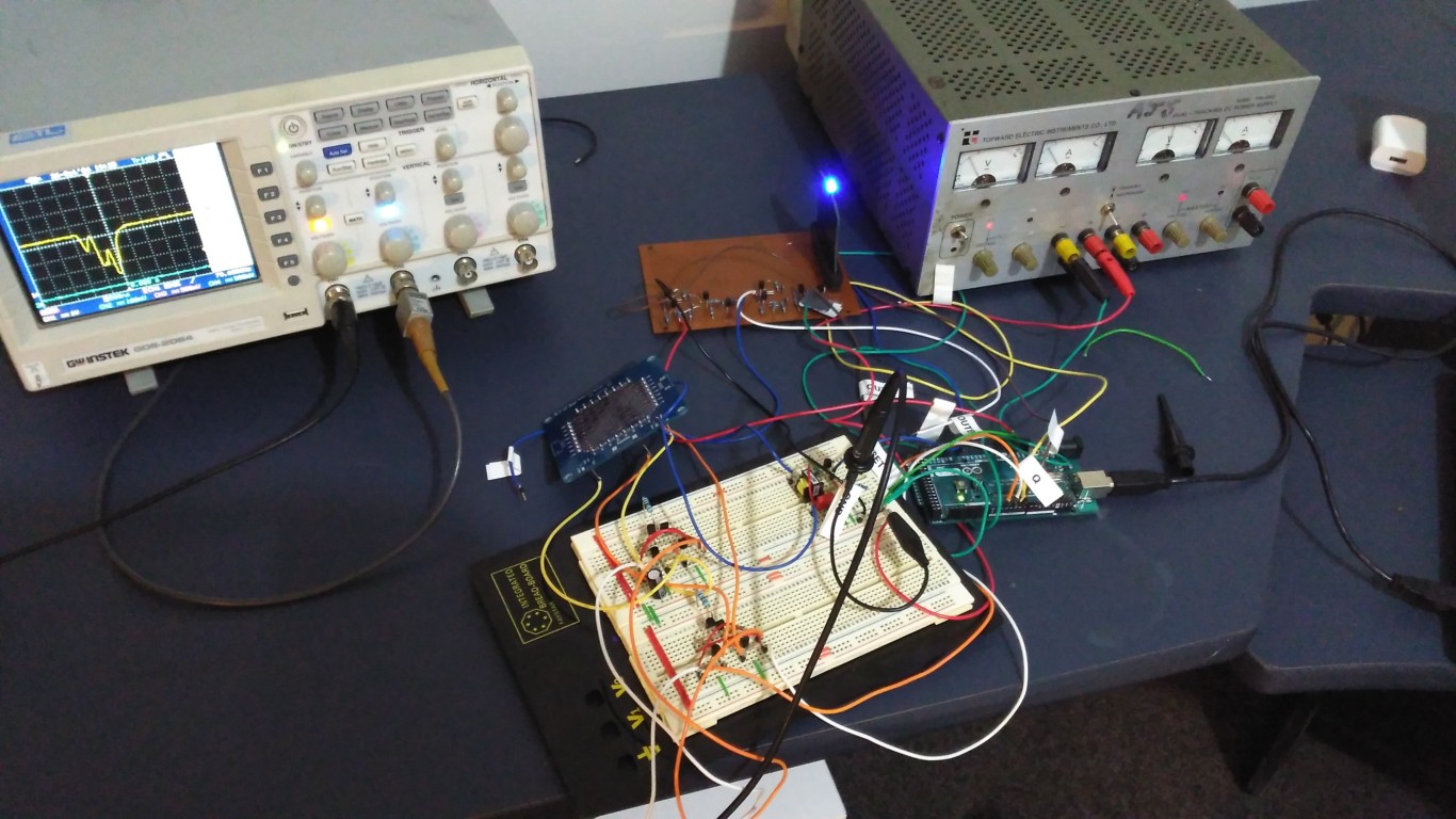
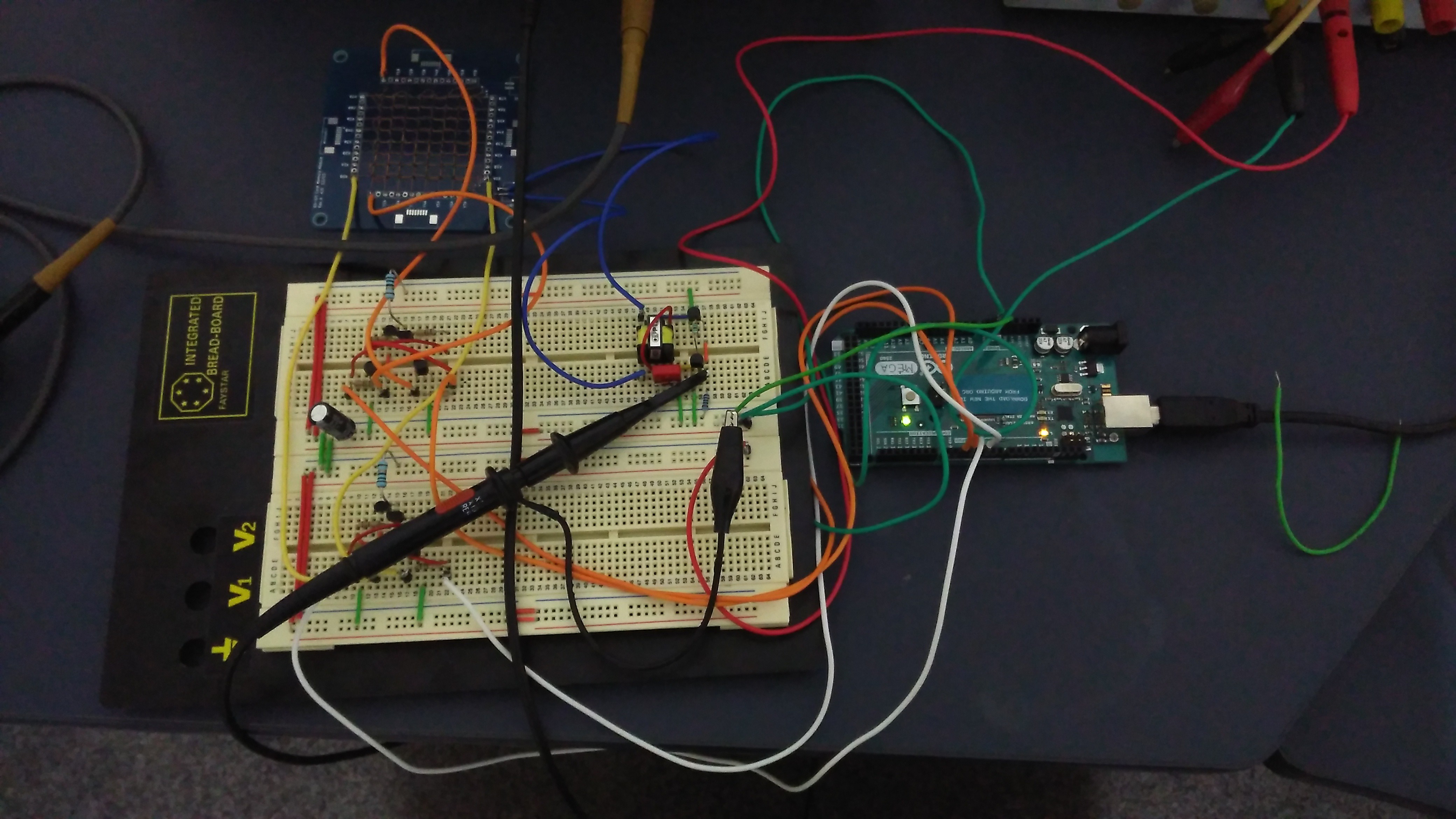
The question is then, would the core selection circuit, H-bridge and core array all play nicely together? I hooked them up with an arduino to generate the control bit and selection signals. I further added a D-type flip-flop module to capture the output from the sense amp:
![]()
So we have:
Arduino -> core selection -> H-bridge -> core array -> sense amp -> flip-flop -> Arduino
I wrote a small program to have the arduino to continuously write a '0' to the core array, then read the array, write a '1', read the array, write a '0'...etc...and report an error if what was read didn't match what was written.
...and success! It seems to work extremely reliably, on all the cores that I have checked. Disconnecting either of the drive lines to the selected core causes errors to be generated, which verifies the coincident-current mechanism that is the basis for this type of memory.
The core switching takes about 1.25us, which seems about right.
To do next:
- build the 8 core planes into a complete module and repeat the arduino test - the planes will be wired in series and I want to make sure this doesn't cause any issues
- test the functionality of the inhibit lines
- build up core selection, H-bridge and sense amp modules
- design and build the memory module carrier board
-
Ay-Ell-Yoo
03/24/2016 at 06:57 • 0 commentsI've added a diagram of the ALU to the Details section. It has 5 functions: bitwise AND, bitwise NOT, Add with carry, decrement, and passthrough. The first 4 fuctions are obvious enough and map directly to opcodes. The last, passthrough, may require some explanation. Passthrough makes the output the same as the A input. This function, in combination with the 4-way mux on the A input, supports the @ and ! memory storage opcodes, and the >R and R> opcodes which shift data between the Data and Return stacks.
For example, set the multiplexer to [T] and the ALU function to Passthrough. [T] is the data from RAM or I/O (depending on the high address bits) at the address held in T. This data is now passed through and the address is replaced by the memory contents held at that address (similar to how the Forth '@' command works). The Passthrough function in this case avoids the need for an additional register to address the memory.
-
Some housekeeping
03/20/2016 at 07:50 • 0 commentsFirst of all, the overall design has been radically changed to something simpler and, I think, more elegant. See the 'Details' section for, well, details. There's a new architecture diagram and I have included a summary of the instruction format and opcodes.
Secondly, I have begun to release design files, starting with the logic gate modules. You'll find the KiCAD schematic and PCB files, as well as gerbers suitable for sending to a board house.
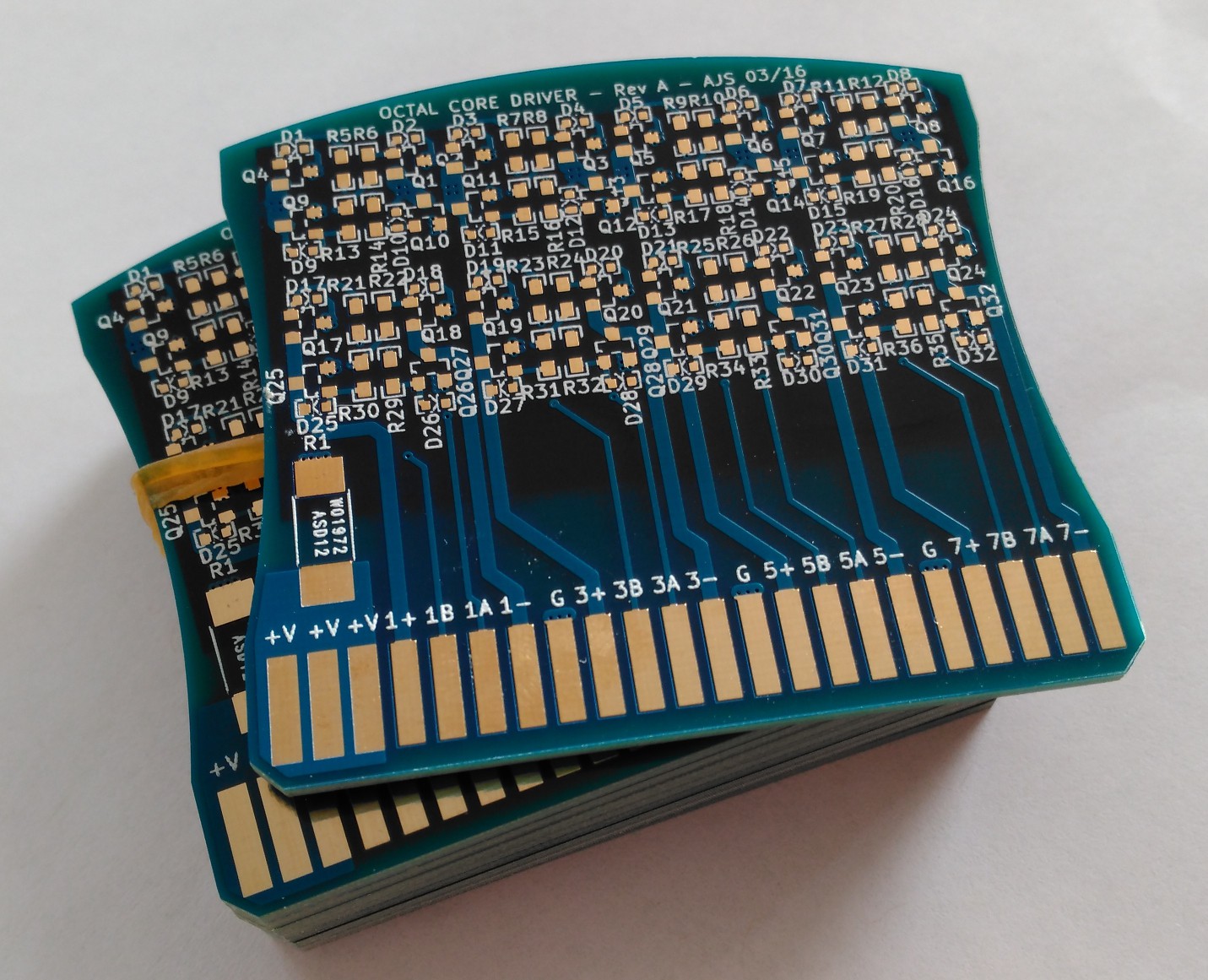
Lastly, I have just received the PCBs for core H-bridge drivers. There are 8 per module:
![]()
These drivers will need additional logic to set the individual H-bridge directions. This logic in turn will be controlled by the data state (whether we are writing a '0' or '1') and gated by the row/column address decoder outputs. I am currently prototyping the H-bridge control logic.
-
Memory cores: first experiments
02/16/2016 at 09:17 • 0 commentsFirst off, I ought to point out that I'm far from the first hobbyist to experiment with memory cores. Here are a couple of pages I've found very useful:
And of course, a moment's googling will yield a wealth of further historical and technical information.
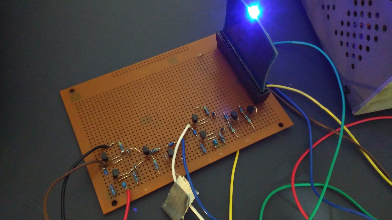
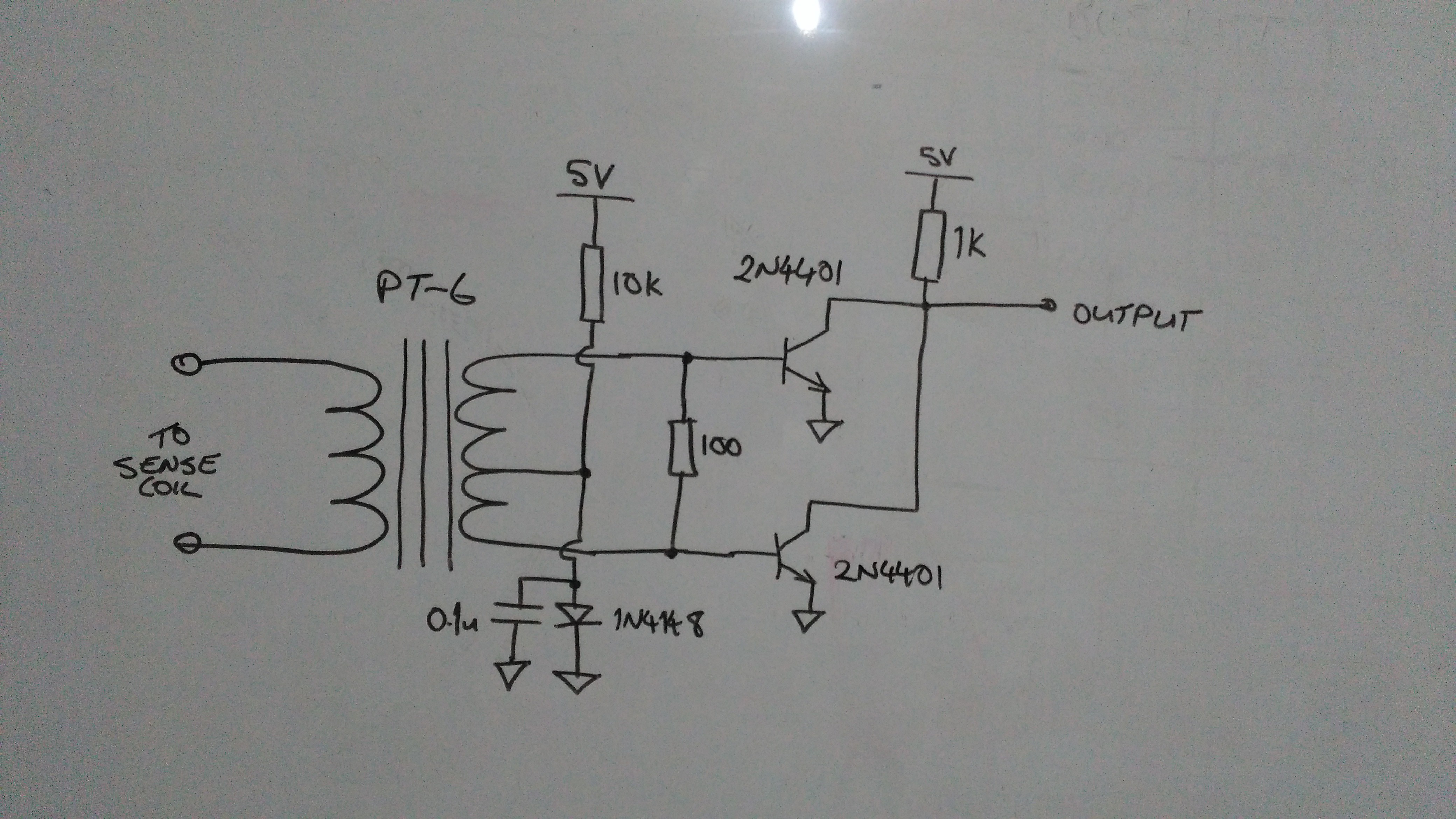
I lashed together a couple of H-bridges to drive the select lines for a single core in the core plane, and a sense amplifier to pick up the switching transitions:
![]()
The H-bridges are pretty rudimentary, here's the schematic:
![]()
The sense amplifier is a tweaked version of Wayne's:
![]()
The above amplifier is the end product of some extensive experimentation. It has a relatively clean output, which I think I'll be able to feed into my logic 'as is' without any further gating for noise immunity.
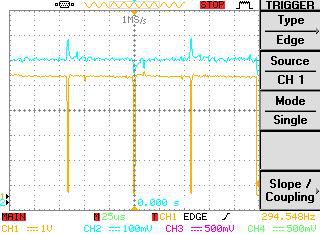
I set up an arduino to drive the H-bridges to continuously write a '1' to a core followed by a read. Here's a scope capture of the sense coil signal (measured over a 470R resistor terminating the pulse transformer secondary):
![]()
The big spikes are the core transitions as the magnetic orientation flips back and forth. The smaller blips are artifacts caused by the magnetic fields generated by the select line currents themselves.
And finally, here is a scope capture of the output of the sense amplifier (orange trace), with the corresponding sense coil signal (blue trace):
![]()
As you can see, each core transition results in a negative-going pulse. I should be able to feed this output straight into, say, the clock input of one of my D-type flip-flops (although I haven't tried yet).
Next:
- check sense amp output can drive logic
- test functionality of inhibit coil
- extend prototype system to be able to drive every core in the plane
- further extend prototype system to be able to drive multiple planes in a 'stack'
Lots to do!
-
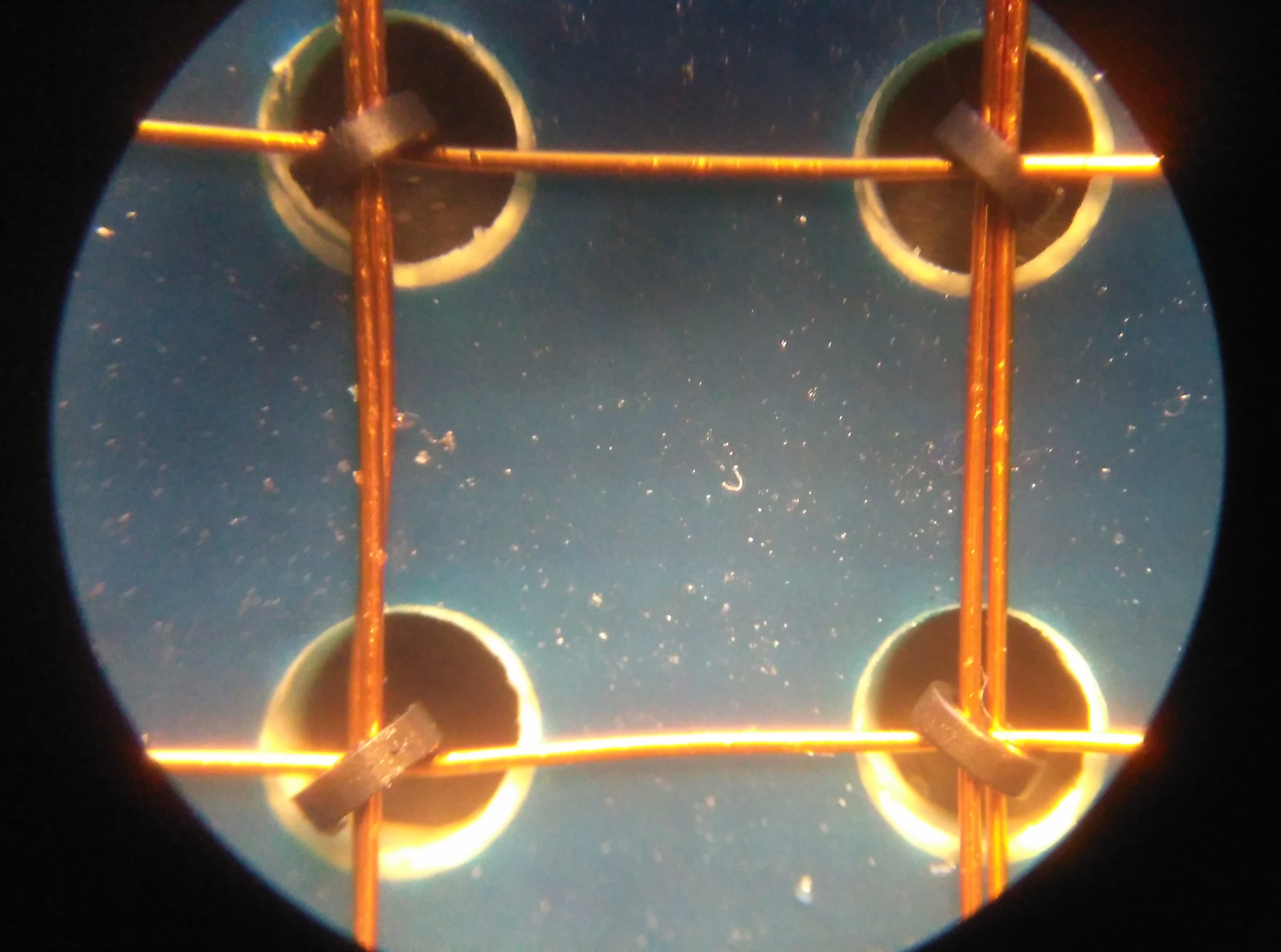
Trial Core Plane ready
01/22/2016 at 21:08 • 2 commentsI've populated one of the core planes to experiment with. I've discovered it's quite tough getting that 4th wire threaded, so I will try a 3-wire system i.e. the sense and inhibit circuitry with share the same wire.
![]()
![]()
The next step is to put together some current drivers and sensing circuitry.
-
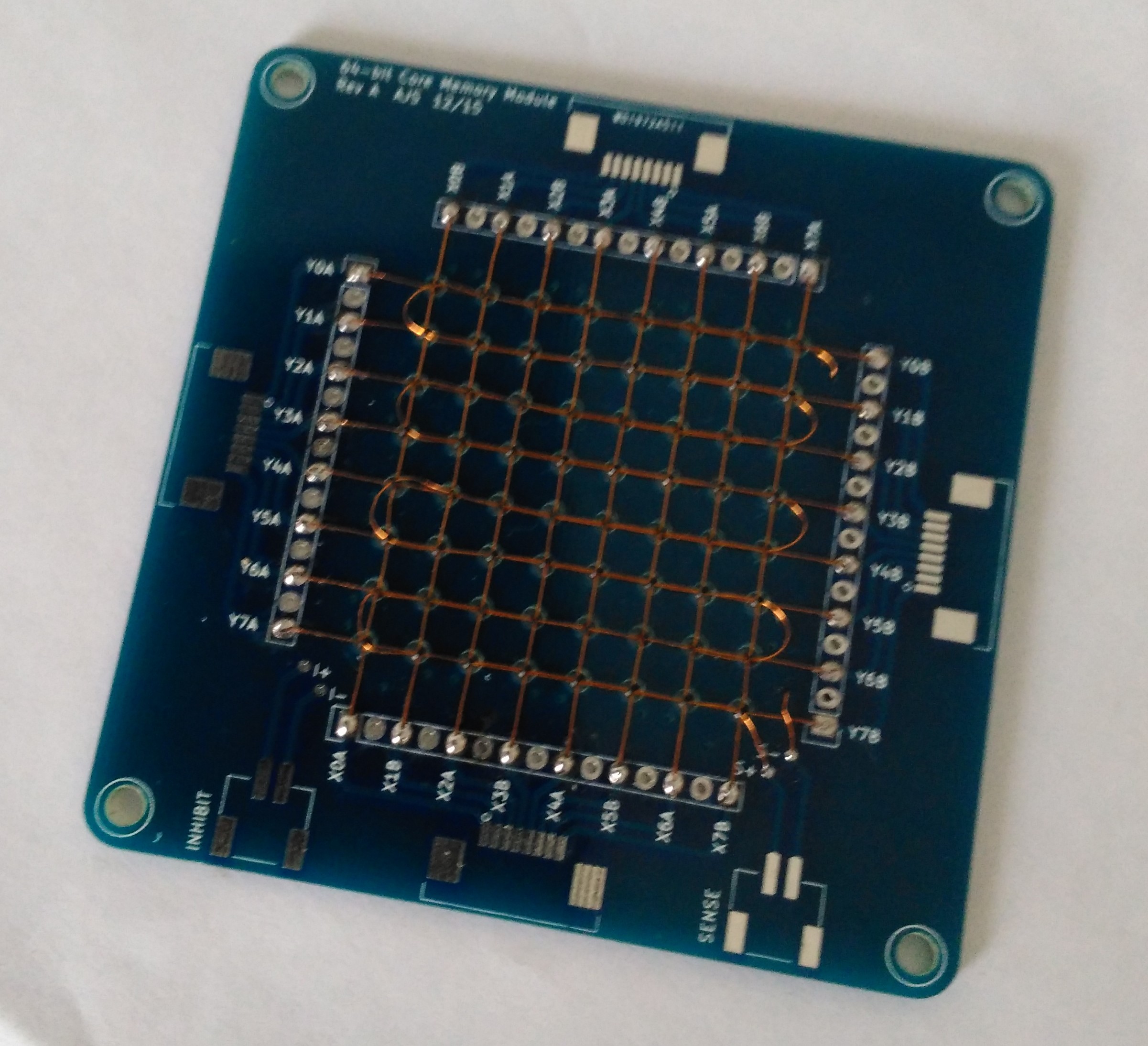
Core Memory Plane PCBs
01/20/2016 at 08:35 • 3 commentsI've just taken delivery of the PCBs for the 64-bit core memory planes:
![]()
The cores themselves will reside in the central holes, with the X and Y select lines running between the pin headers. There are 4 FFC (flat flexible cable) connectors around the outside for running the X and Y lines through the stack, and 2 JST headers on the left for the SENSE and INHIBIT lines.
8 of these PCBs will stack to make a 64-byte memory, and the stack will plug into a panel via pin headers on the bottom plane. The panel will have the line drivers, sense amplifier and flip-flops for shuttling data in and out of the memory.
I will need to do some experimentation with a single plane before proceeding to the final panel design.
-
Data and Return Stack address decoders
01/17/2016 at 05:22 • 5 commentsThe stack decoders are now complete and mounted in the frame:
![]()
The yellow lights are indicators for the row and column output drivers.
ED-64: A discrete 8-bit computer
ED-64 will be an 8-bit computer built with discrete components, and will feature a ferrite core memory (documented as a separate project).