Andrew Starr
-
Core Blimey
12/08/2015 at 06:45 • 8 commentsI'm in the process of finishing some 2-to-4 decoder modules for the first stack address decoder, and building up a second one. But I'm also starting to think about the core matrices themselves as it will soon be time to work on them.
One of the questions to answer is: a 3-wire or 4-wire system? A 4-wire system (X, Y, Sense, Inhibit) is easier but of course means threading 4 wires through each core. In a 3-wire system, the sense and inhibit circuitry share the same wire. This complicates the electronics a bit, and also requires that the sense/inhibit line be threaded in a way that reduces noise immunity during sensing.
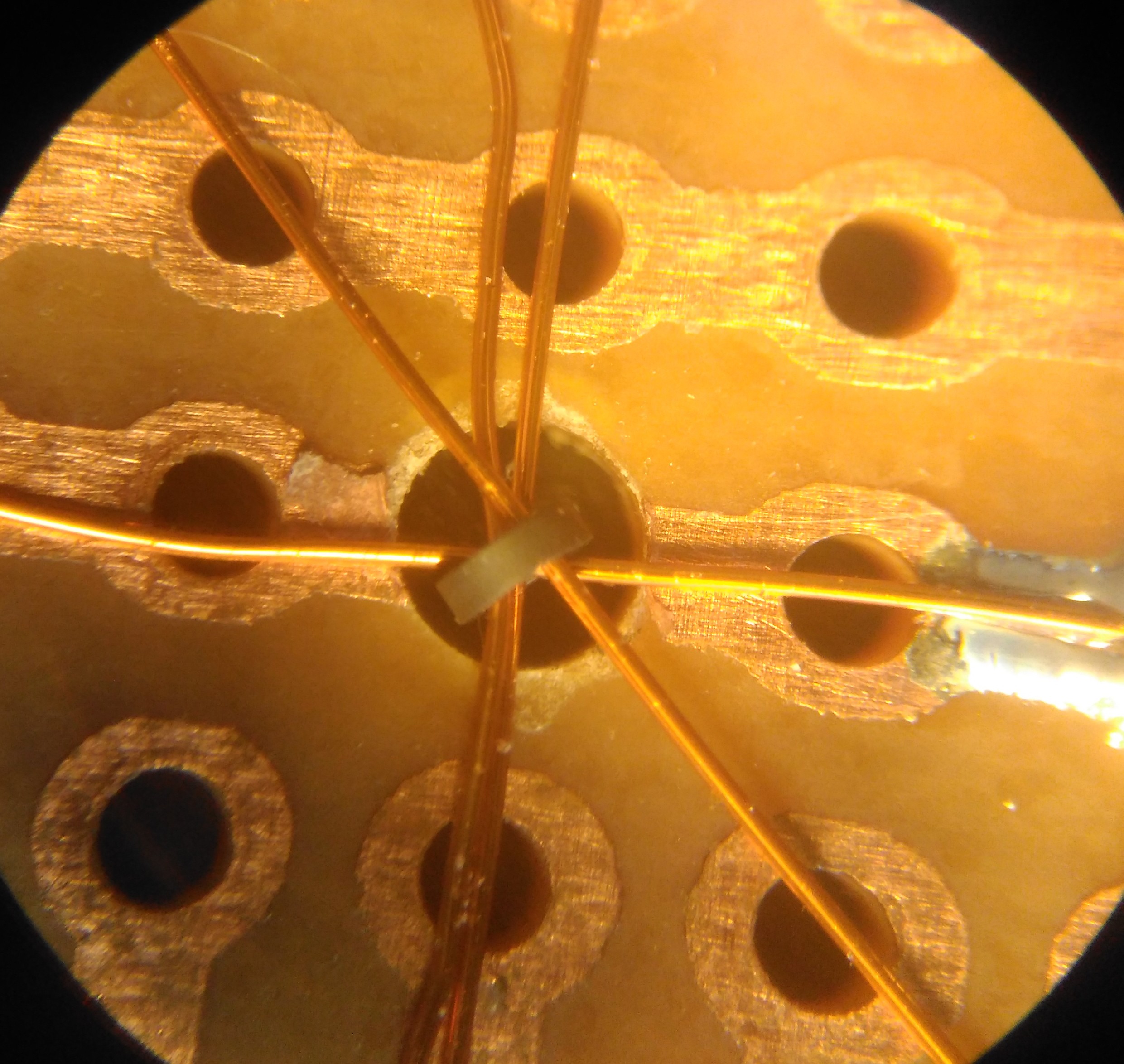
So I did a quick test on a piece of veroboard to see how easy it would be to get 4 wires through a core. It turns out that it's not too bad:
![]()
This image is taken through a 30x microscope (which I use when I'm hand-soldering SMDs). The central hole that the core is sitting in is 2mm in diameter. The wires are 0.16mm in diameter. The horizontal wire is X, the 2 vertical wires are Y and inhibit, and the diagonal wire is the sense wire.
So, a 4-wire system it is.
-
Stack Address Counter: Some Numbers
11/25/2015 at 09:29 • 6 commentsToday I did some voltage, current and speed tests on the newly-completed counter section:
Supply Voltage (V) Maximum Clock Frequency (MHz) Average Current Consumption at Maximum Frequency (A) 5.0 1 1.0 3.3 1.5 0.8 2.7 2 0.6 It's interesting to note the effect of slew rate when comparing supply rail vs maximum clock speed. So lower voltage is better in this regard. However at 2.7V the LEDs are starting to dim, and since 1 MHz is my target clock speed, 3.3V seems a good compromise.
Now I have to make some 2 to 4 decoder modules to generate the row/column signals from the 6-bit address...
-
Holy Crap, it works!
11/24/2015 at 08:07 • 1 commentFirst powerup of the counter section of the first stack address decoder board:
-
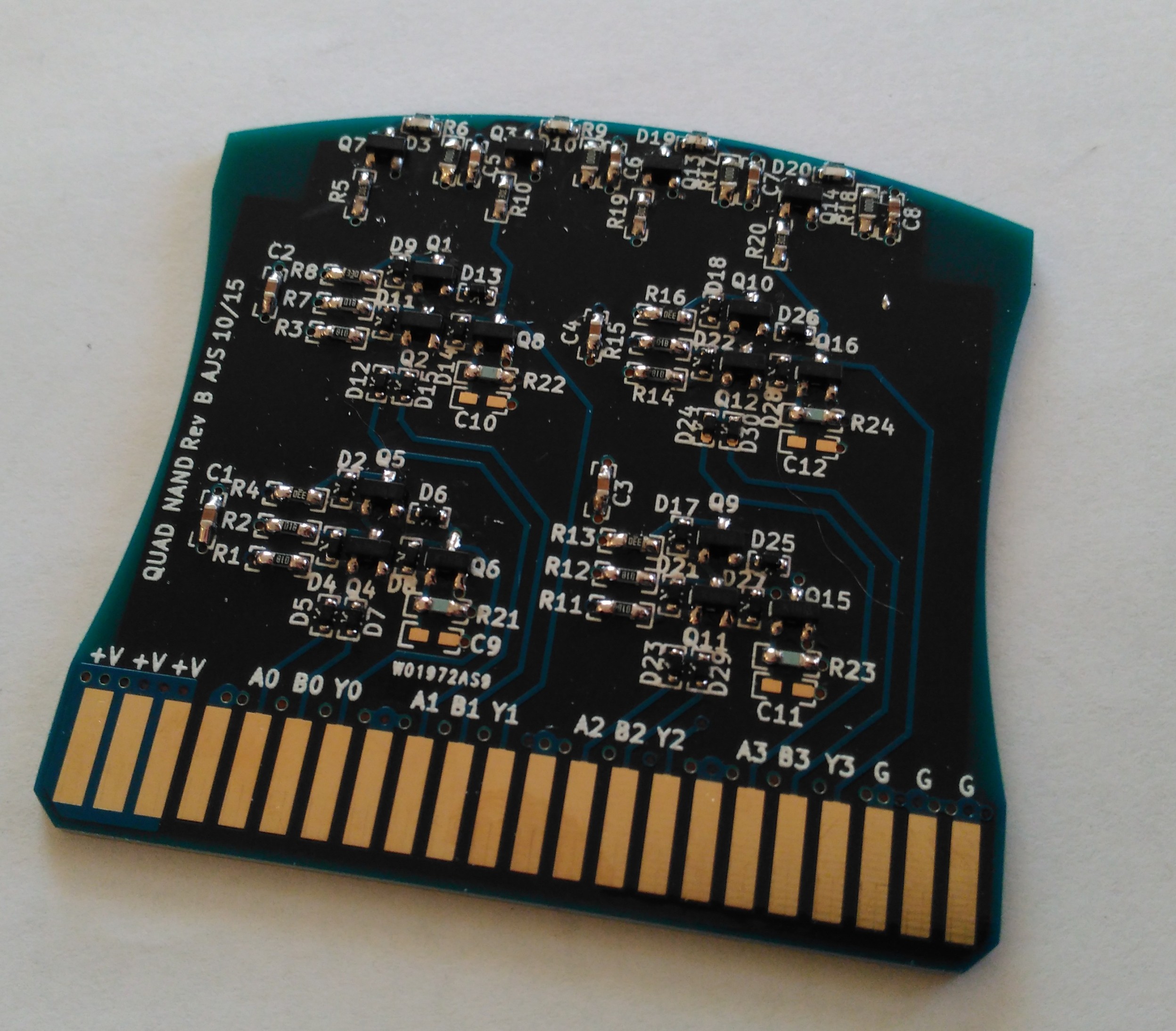
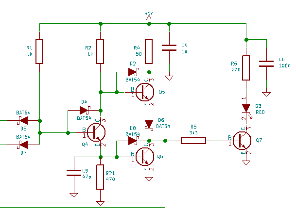
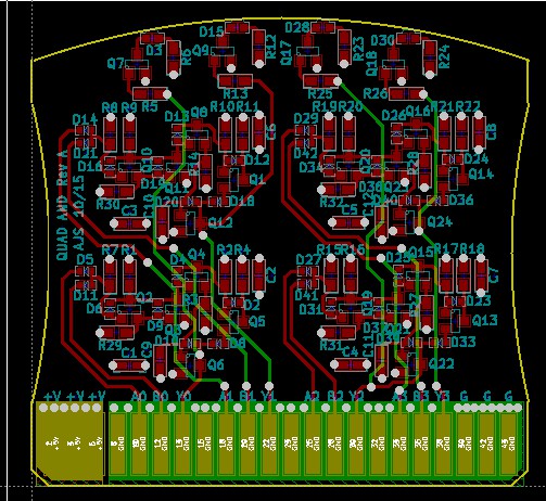
Quad 2-Input NAND Gate
11/23/2015 at 07:47 • 3 commentsThe first NAND module has passed testing:
![]()
![]()
A screencap of the schematic of one of the gates (1/4 of the module):
![]()
As you can see, it is basically my standard complementary-driven totem pole output, with a couple of schottky diodes in a wired-AND input configuration.
Almost ready to start populating the stack address decoder panels....!
-
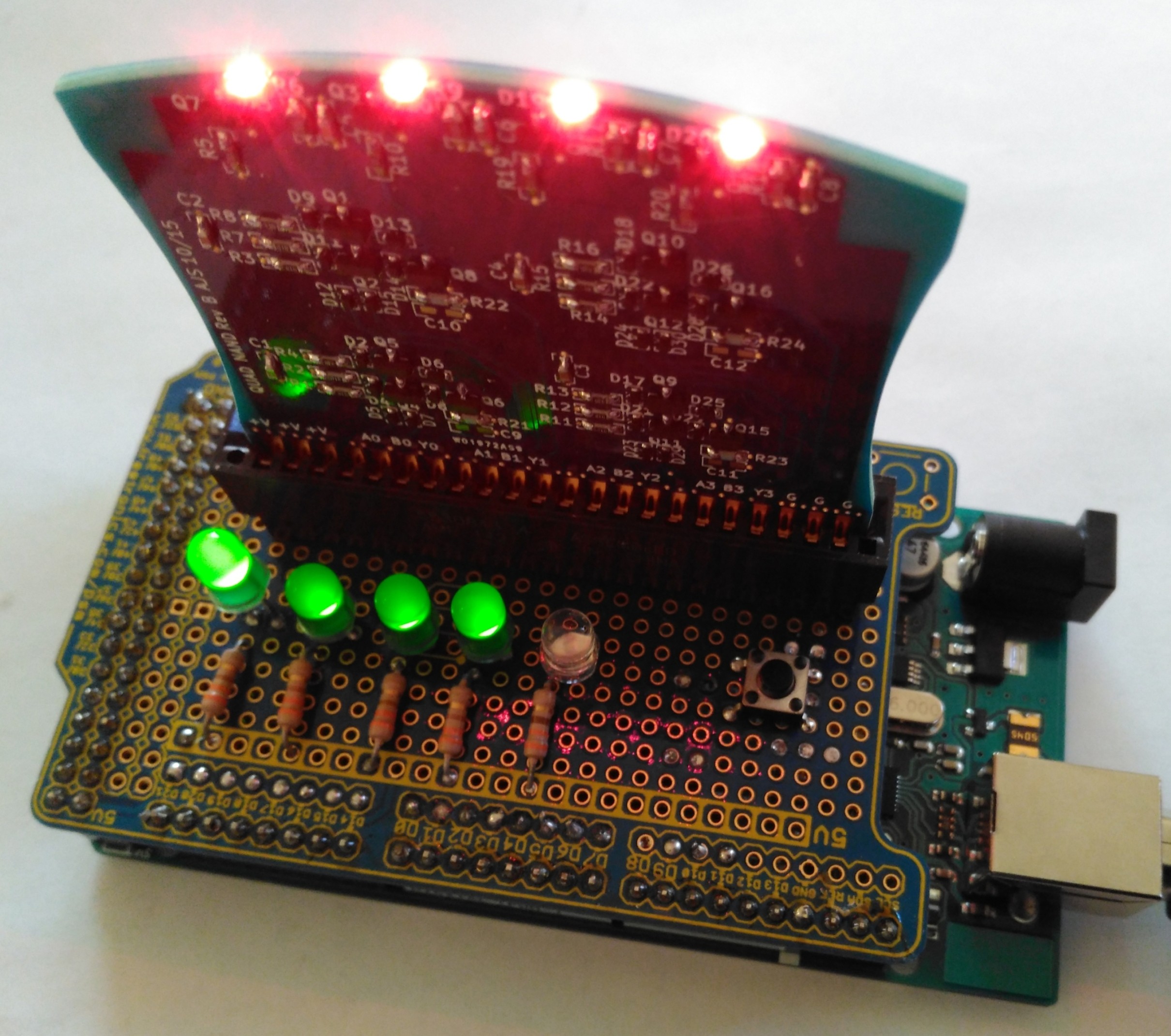
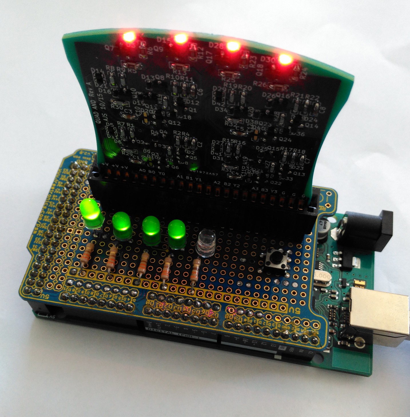
AND gate passes testing
11/05/2015 at 02:17 • 4 commentsI modified the FF jig to test the AND gate I had soldered. The jig tests each gate with all 4 binary combinations of input, and looks for the correct binary result. 4 green lights = 4 good gates:
![]()
Each gate has a red LED to indicate output state.
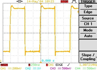
I also did some speed tests. Here's a gate output waveform with both inputs driven by a 1 MHz square wave:
![]()
and at 2 MHz:
![]()
some over/undershoot present but not too bad. There is provision on the module for loading some capacitance to smooth it out if necessary. I would have liked to have driven it faster to find its maximum switching speed but my signal generator only goes up to 2 MHz.
Finally, I wanted to see some lights blinking so I wrote some crappy arduino code for the jig to do it:
-
Happy Birthday, Mr Boole
11/03/2015 at 06:05 • 1 commentThere has been a hitch in arranging a stencil for the AND gates (thanks for nothing, Paypal) so I have hand-soldered the first one to test the design:
![]()
Next up, a jig to test finished AND, OR and NAND gates. I also intend to whip up a carrier board to do some speed and propagation delay tests.
Also, I have repaired the 4 faulty flip-flops from my first batch of 20. The usual problems - diodes around the wrong way, missing resistors.
-
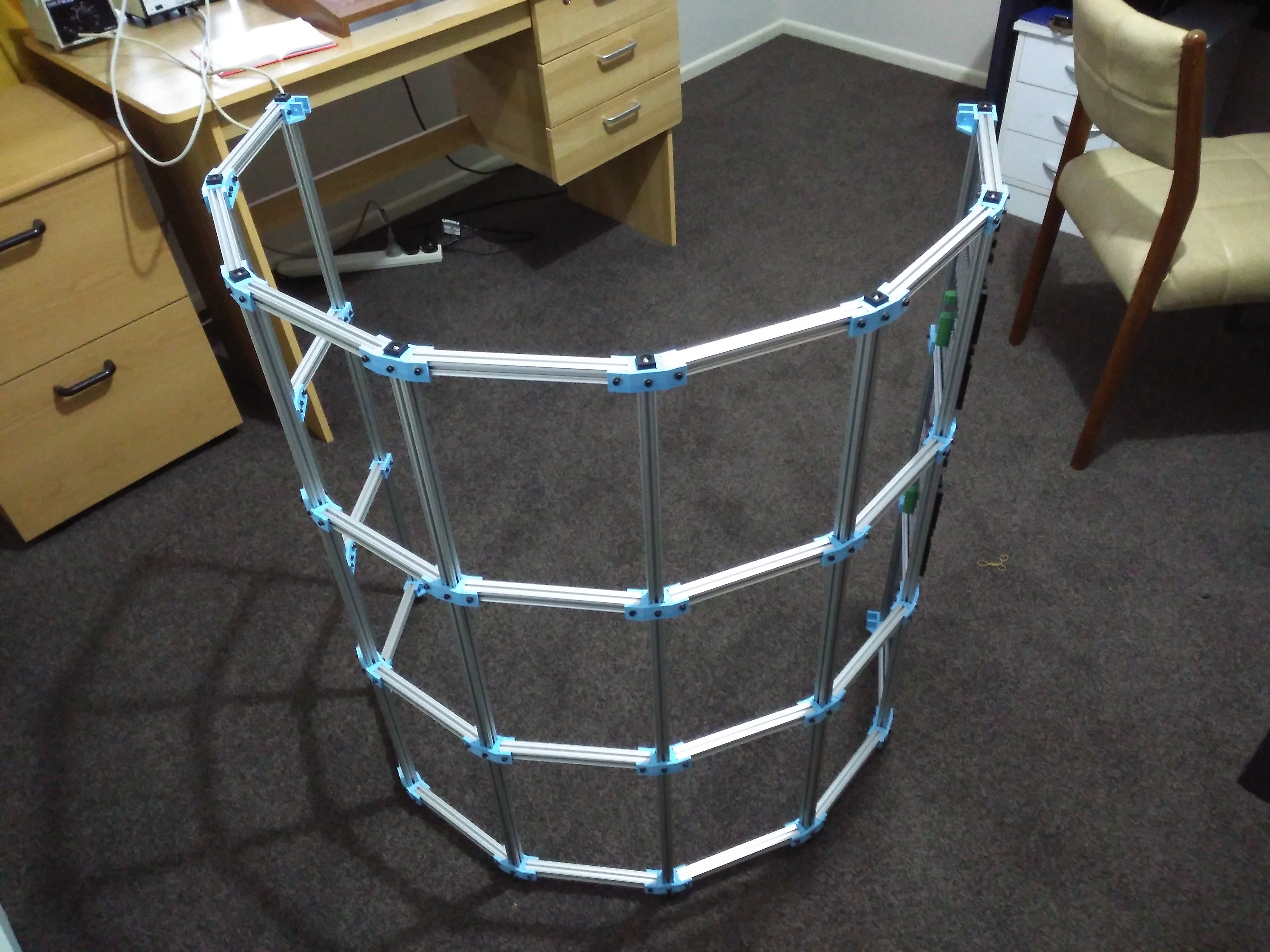
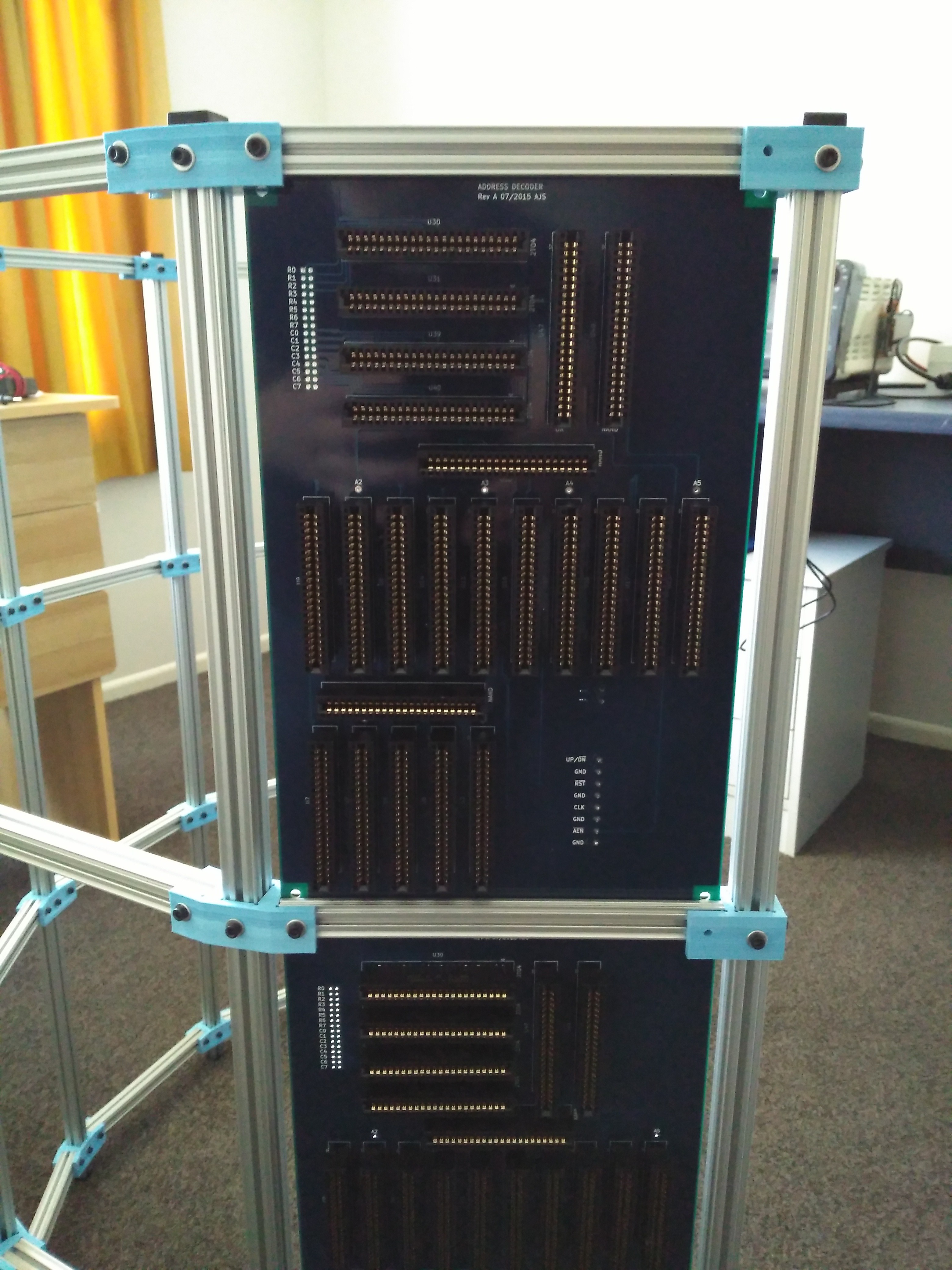
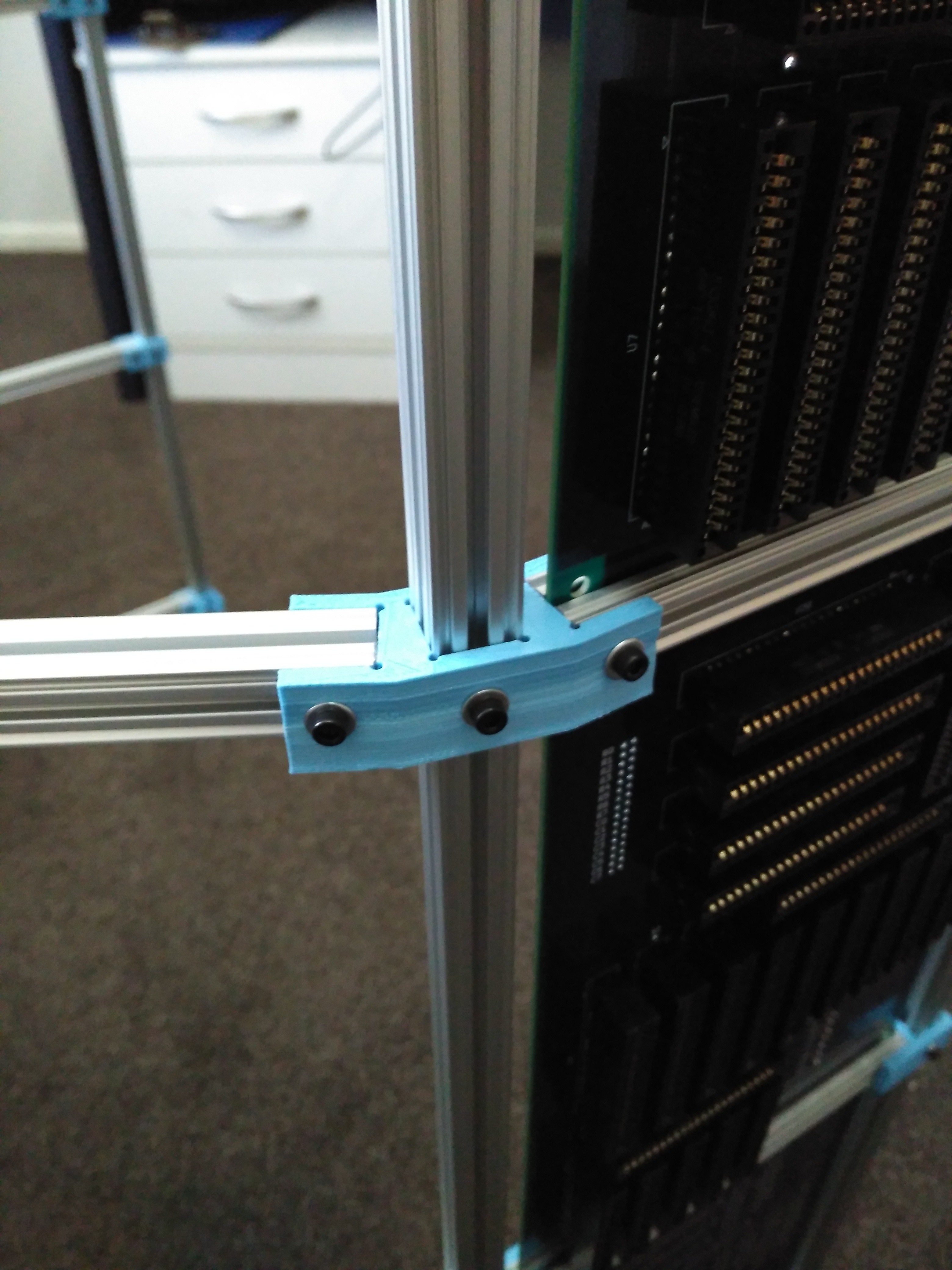
Mounting frame (almost) complete
10/17/2015 at 22:41 • 3 commentsIt's missing a few screws (like its creator), but the frame for mounting the boards is largely complete:
![]()
![]()
Each 'cell' in the frame can carry a 177mm wide by 275mm high PCB. The inter-module wiring will be run along the interior sides of the beams, and the logic modules, memories and operator interface will face the exterior.
Here are a couple of shots illustrating how the module panels are held in the frame:
![]()
![]()
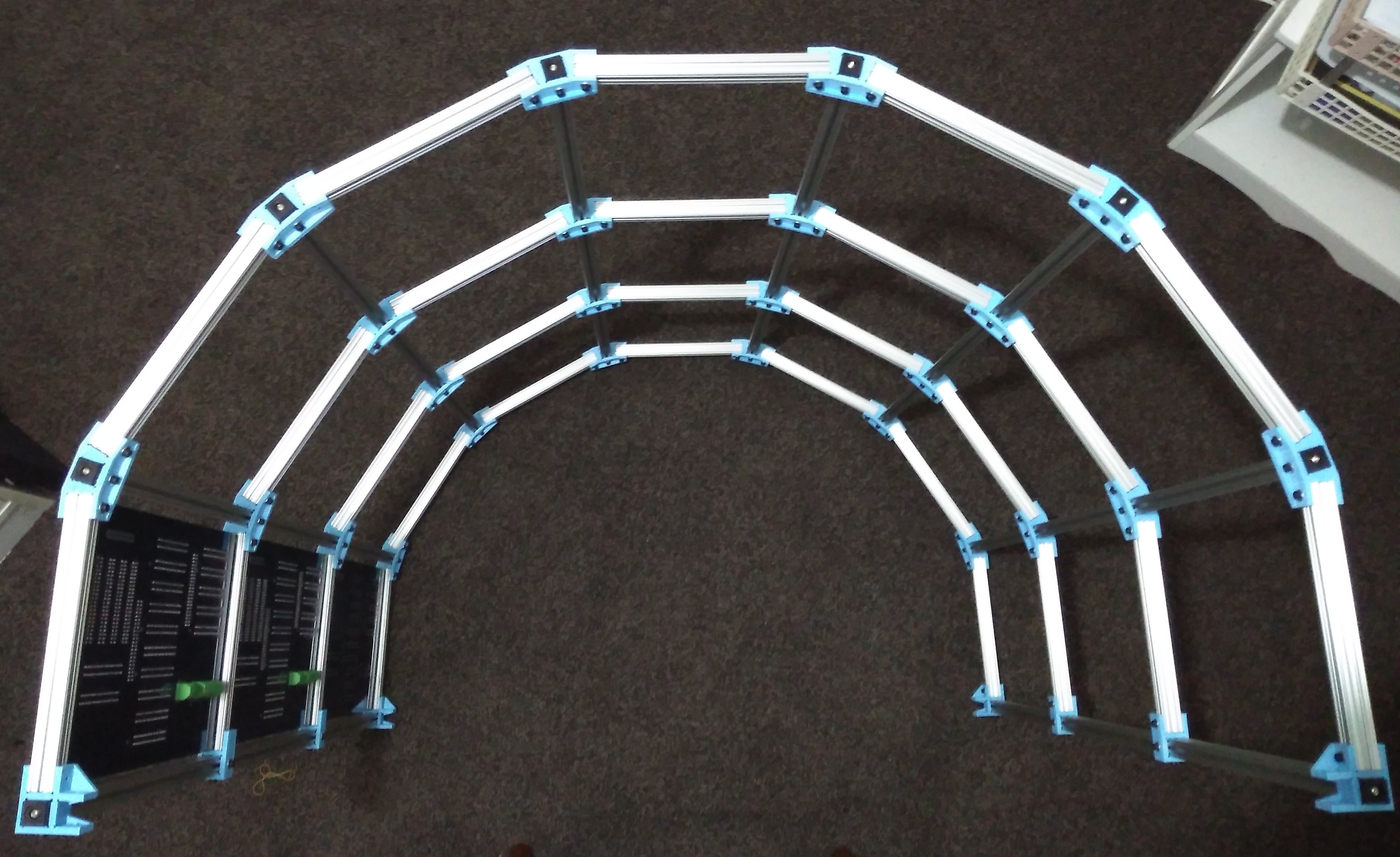
There is provision for a top and bottom cross-beam to give the structure extra rigidity if I decide it needs it:
![]()
-
Quad 2-input AND gate PCBs have arrived
10/12/2015 at 06:04 • 0 comments20 AND module boards now waiting to be populated:
![]()
-
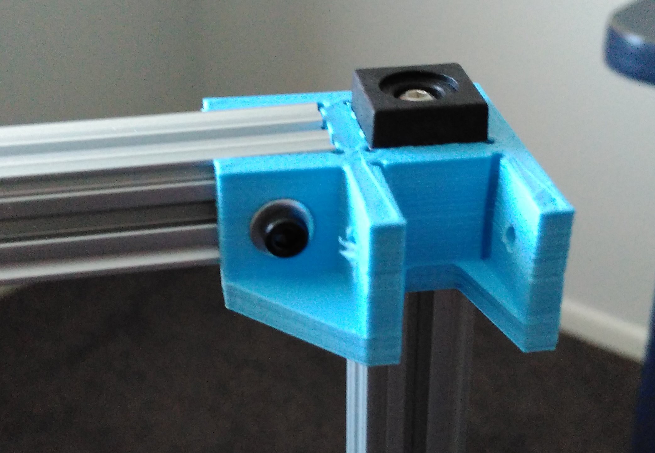
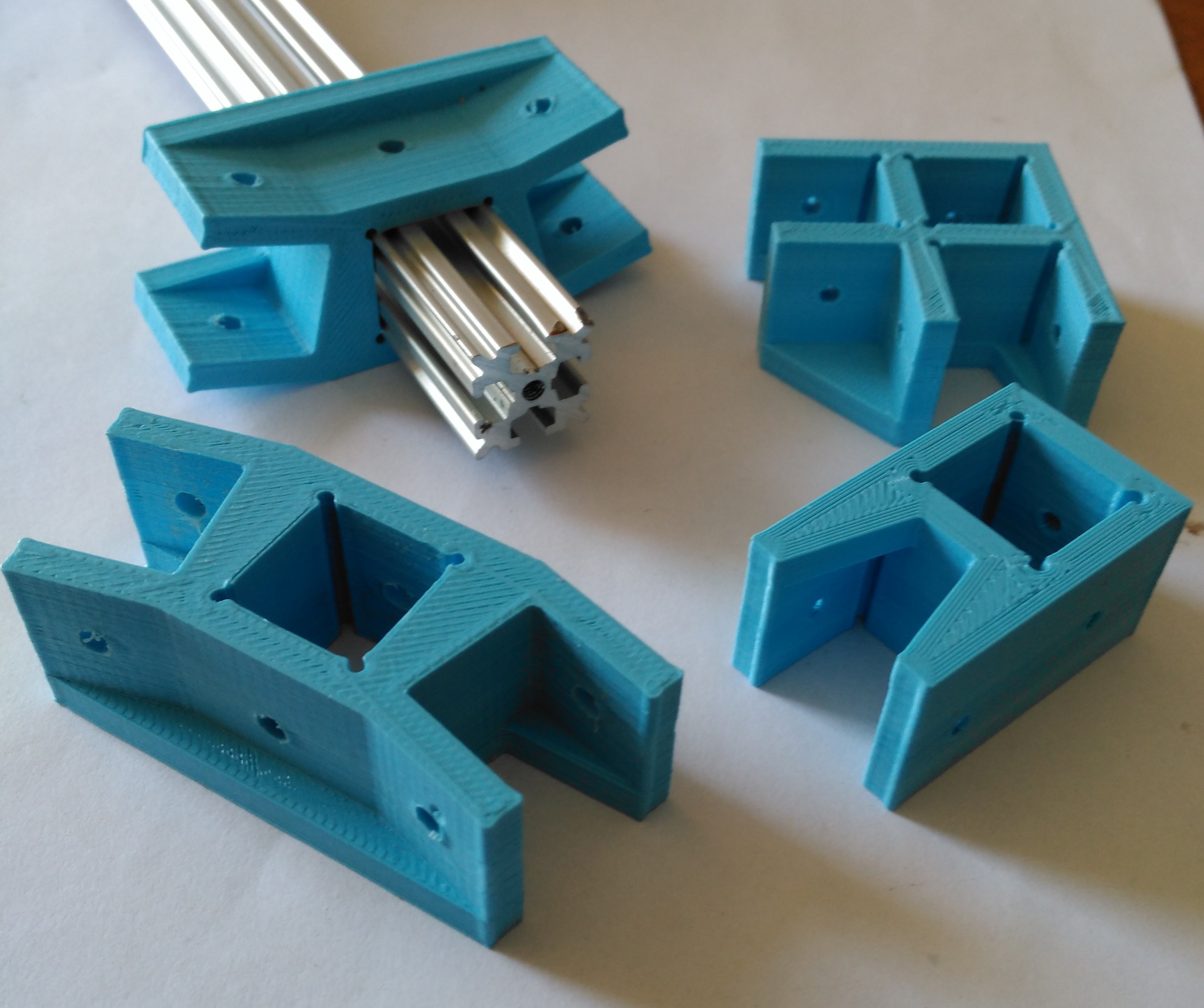
Brackets 'n' Beams
10/11/2015 at 04:23 • 0 commentsI have opted to mount the electronics in a frame constructed from Openbeam extrusions. The extrusions themselves are from Makershop here in NZ. The frame will consist of 7 facets fixed in a semicircular arrangement. Each facet will hold vertically 3 backpanels. This will provide a good view of everything and allow easy access to wiring.
TTN has printed that last of the brackets I need to put the frame together (thanks Jotham!). I designed the brackets with LibreCAD and OpenSCAD.
![]()
Shown in the photo are brackets for mounting 2 horizontal extrusions to a vertical one at 30 degrees, a 90 degree corner bracket and a bracket for butting a horizontal extrusion against a vertical one.
-
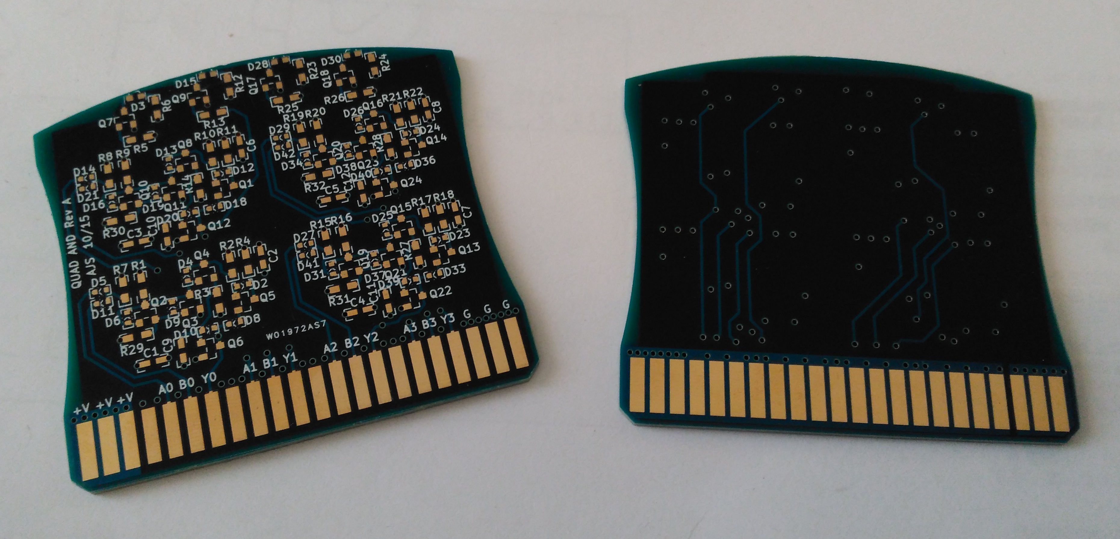
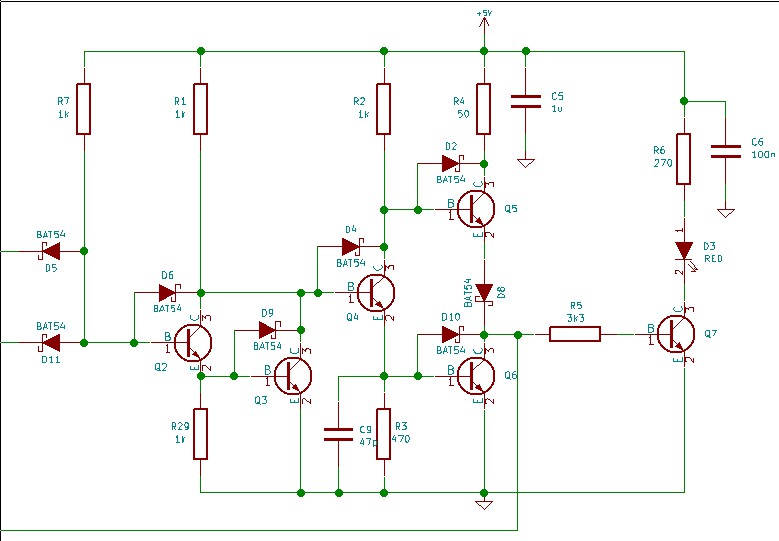
Quad 2-input AND gate
10/05/2015 at 06:54 • 2 commentsThe current task is to get the stack address decoder boards populated with the required logic modules. The flip-flops have been made and tested, next up are the AND gates. The PCBs are currently being made by pcbway. Here's the schematic for a single AND gate (there are 4 of these on a module board):
![]()
According to LTSpice, this gate design should be good for several MHz, with an average current consumption of 10mA (driving 1 downstream gate input).
Here's a screencap of the PCB (power and ground planes turned off):
![]()
ED-64: A discrete 8-bit computer
ED-64 will be an 8-bit computer built with discrete components, and will feature a ferrite core memory (documented as a separate project).