mosaicmerc
-
Double Sided using fresh HP toner @ 360F
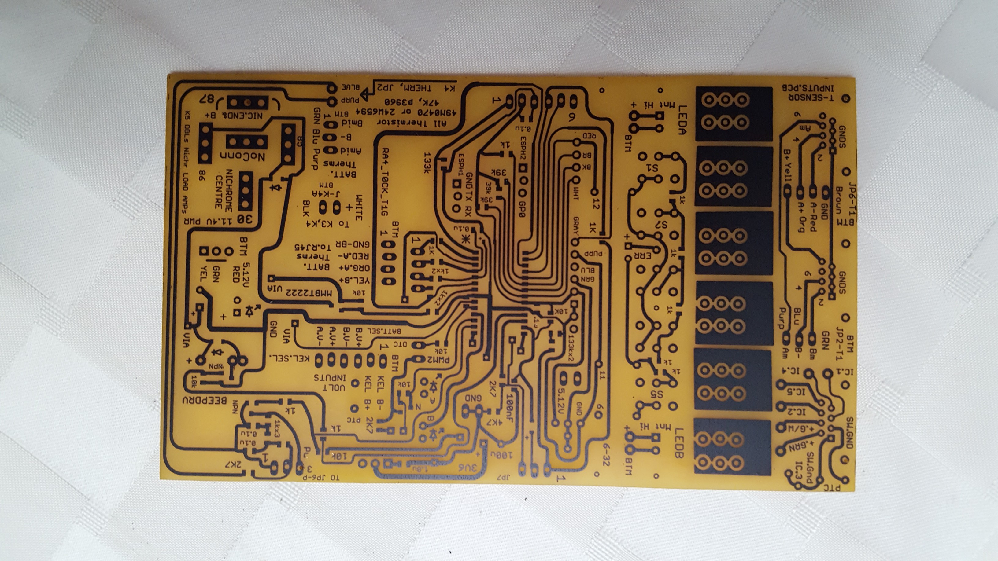
10/27/2017 at 03:10 • 0 commentsDid a test with a bit more heat with a fresh OEM HP toner cart for the 1102W printer.
Very solid transfer and etch, no pin holing in the fills , did not use the extra foiling step. 5.5" x 3.25"PCB with SOIC part (28 pin) in centre and 0805 SMT parts.
Also on ALIEXPRESS search for M0.9*2.5 Copper Hollow Rivet , to make handling vias simple.
![]()
-
PCB slicing dust vacuum
04/12/2016 at 17:33 • 2 commentsWell, PCB dust is an issue with the diamond cutting blade on the mini table saw . But it is so good at shaping and trimming PCBs that I upgraded the operation with a mini vacuum. An
ArmorAll AA255 ...from Amazon, $39 for 2.5Gallon capacity.
Now the mini saw sits in it's close fitting original box with a round hole in the side of the box for the flex vacuum hose to snug in. Works a treat, the dust is pulled in via the negative pressure in the box. The vacuum is also very good at cleaning up the swarf from the Dremel or Proxxon drill cuttings & grindings. It has serious suction, that includes metal cuttings!
-
PROXXON drill press upgrade
02/27/2016 at 19:51 • 0 commentsWell I caved and purchased a mid tier Proxxon rotary tool and matching drill press and mini vise. I already had acquired a Proxxon KT 70 compound X-Y table before which works with the press as well.
This tool is far more stable, with minimal run out compared to the Dremel 395 and 'plastic' press arrangement I had used to date. Plus it can do 20K RPM and has an independent speed control and on/off switch , which is better than the Dremel's unified control. I don't expect much broken carbide bits now.
I modded the minivise to lock onto the press slide bar for precision work on small parts. 1, 6-32 x 1.5" screw was required.
As with the Dremel I installed a 'back light' for illuminating etched PCB through holes. Basically a Jumbo super bright white LED running off an old Nokia 5V charger & a 220 ohm series dropping resistor.
Note the pics in the upload area.
-
PCB slicing
01/20/2016 at 09:07 • 0 commentsWell, my days of scribing and snapping PCBs are now over. Was a bit inaccurate and FR1 boards have a nasty chance of splitting.
With this 4" table saw (portable desktop) unit:
http://www.amazon.com/gp/product/B00AEZ70AO?psc=1&redirect=true&ref_=oh_aui_detailpage_o00_s00
I can get precision, repeatable cuts at the cost of about 1/16" of PCB 'loss' when using the diamond blade as supplied. The cut is smooth and precise.
Cutting with the toothed 'wood' blade also works but isn't as clean, causes copper swarf and about 3/32" of PCB is 'lost'.
Highly recommend it! Blade swap in about 2 minutes with a pair of spanners or sliding wrenches.
I cut the box it came in down to about 3" tall to place the whole unit inside and 'contain' all the 'dust' & 'dross' from the cuts....barely any back splash of dust that way.. I plan to make a custom variable 'fence' with my laser cutter. But a couple of small G clamps and a bit of 1/4" alum. channel is good for a quick adjustable fence at any time.
Now I can make custom fit RF cavity filters using PCB material....how's that for a hack?
-
Full Spectrum 40 W 5th gen' hack' fix
12/03/2015 at 17:00 • 0 commentsFor those of you using this laser, you'd note that the you tube alignment videos for the optics/ mirrors don't emphasize that centering the beam in the lens as important.
Well in vector cutting, it is important as noted here:
http://www.buildlog.net/blog/2013/05/why-are-my-laser-cut-edges-not-straight/
Although I had a perfect mirror alignment of the beam I still had this angled vector cutting problem....as the beam wasn't quite centered.
I had to
1) Adjust the nut and screw axle arrangement on the top roller pair to 'push' the z-axis top towards the front of the laser machine. this straightened up the sloped cutting parallel to the gantry.
2) Drill a NEW pair of 1/8" holes for the laser lens assy to attach to the Z-axis vertical adjustment, shifting the lens assy to the left by 1/4" relative to the mirror above it. This located the laser beam in the centre of the lens.
3) Drill and tap a pair of holes on the mirror above the lens to provide a 4 point mounting instead of a 3 point mounting for better mirror adjustment control. This proved to be not essential with the other mods in place.
4) Loosen the 3 silver hex screws holding the mirror block (above the lens) to the roller transport mechanism and 'twist' the whole z axis (incl mirror & lens) about 2 degrees clockwise, then retighten the 3 screws onto the roller transport. These screws are located under the top rollers facing the laser tube. The clockwise twist works if the slopes of the cuts perpendicular to the gantry go from left to right. Twist the other way if your slopes are right to left.
Items 2,3,4 straightened up the cuts perpendicular to the gantry.
The end result is near square cuts thru 1/4" thick acrylic on all 4 sides and better beam penetration for the same power setting.
They called it a "hobby" laser for a good reason it seems. You can improve it's precision & results with a bit of effort.
-
Thinking 3D additive PCB thoughts
10/05/2015 at 01:07 • 0 commentsHaving automated the doublesided PCB making, I find myself having to interconnect several boards using wire to board components and headers for more complex systems.
Using the same tools to make the double sided board with more leverage on the 40W laser cutter i believe I can design doublesided boards in layered stacks. Building multilayered prototypes in an additive fashion.
Now arduino type stackable modules come to mind, but for true high density systems I am looking at 1/32" thick FR1 PCBs or even flex PCBs which are etched in a manner to permit the 40W laser to cut the base material as required.
Then sidestepping the 0.1" pitch headers, the boards are designed to mate together so that components on the bottom of one do not align with the components on the sandwiching boards. By etching properly and then laser cutting notches for components, it's possible for the boards to lay flat on each other with no spacing!. Using the same stencil cutting technique we can have insulating 'separators' between these sandwiched smt boards. Vias can be soldered in stages as the boards are layered, even blind vias are possible.
Now this approach can potentially give a higher component density than regular multilayered boards as components can actually be 'embedded' inside a board sandwiched by multiple layers with other components stacked above embedded components in it once the intervening board layers offset the embedded component's height.
Consider a sandwich of 4 layers of 1/32" PCBs, then SMT components on the inner side of layer 1 can well be buried completely by layer 4, permitting more components on layer 4 to occupy the same location displaced vertically. Again, insulating laser cut transparencies provide inter-layer isolation as required. By using layer separator insulating material such as acetate transparencies, mylar or kapton sheets (laser cut with required slots/holes) it may be possible to place solder paste dots on different copper layers to create bond points between successive layers to be reflowed after the layer stacking is complete!
The out come of all of this could be a device perhaps 1/2" thick with up to 12 layers of double sided copperclad 1/32" material plus separators and several layers of stacked embedded components. All DIY @ Home, using the techniques described and the on hand tooling!
Faraday cage effects, reduced EMI minimal board inductance, reduced signal latency for high speed digital processing and minimal form factors are all benefits. This brings electronic micro manufacturing a bit closer to home with micro prototyping capabilities!
PCB /SMT MAKER LAB @ Home
This project outlines how to do advanced PCB making at home with proper tooling. Tooling includes a laminator and hobby laser.