Dave Vandenbout
-
Version 0.2 Is Live!
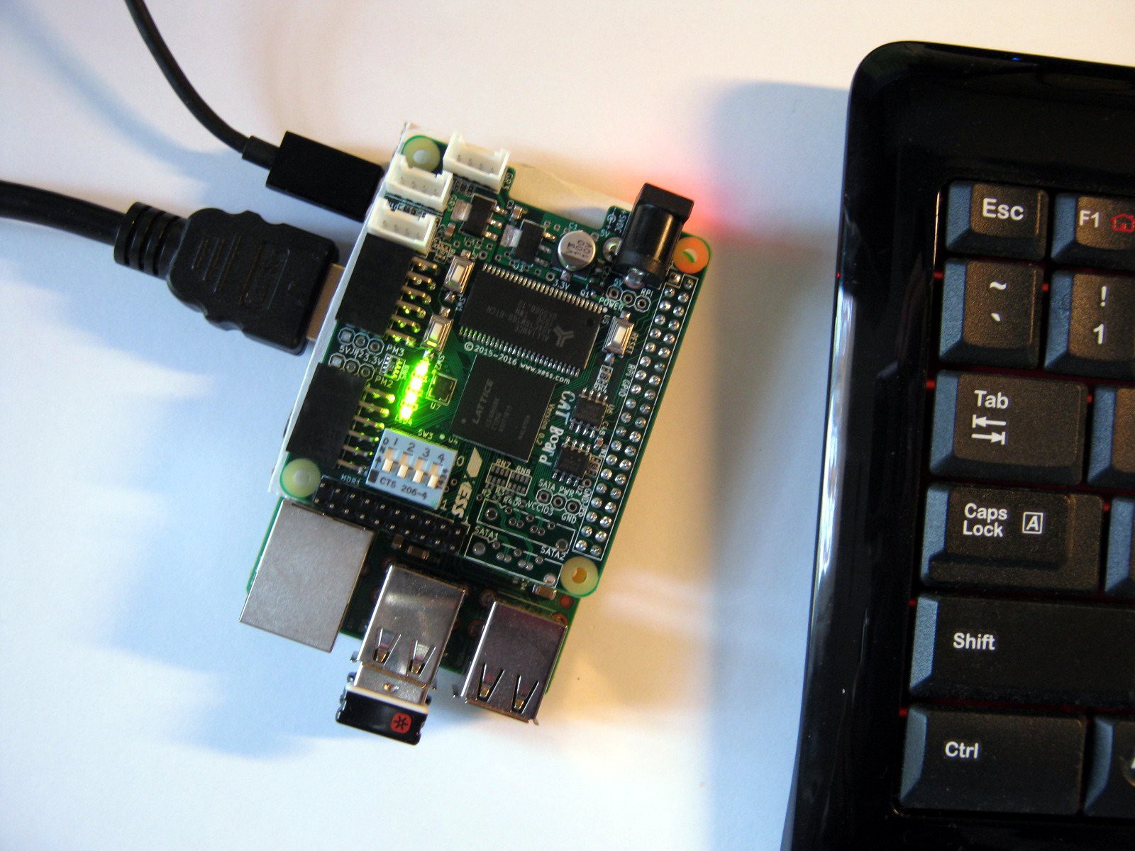
04/16/2016 at 15:17 • 1 commentWell, this doesn't happen often: I assembled the new 0.2 CAT Board and it worked the first time! The Raspberry Pi was able to program it with the SDRAM diagnostic and it passed (showing four green LEDs).
![]()
The next steps are:
- Write the RPi code for programming the bitstream into the SPI flash so I can test the configuration of the FPGA in stand-alone mode.
- Assemble the SATA I/O. (I checked that the SATA connectors fit their new PCB footprints, but I still need to get the correct termination resistors.)
-
Comparison of CAT 0.1 and 0.2 PCBs
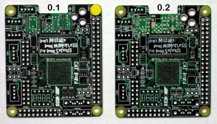
04/14/2016 at 15:17 • 8 commentsBefore assembling a CAT Board with the new 0.2 PCBs from PCBCart, I thought I'd compare them to the previous 0.1 version from PCBWay.
At a macro-level, they both look like circuit boards. No discernible difference. So that's good.
![]()
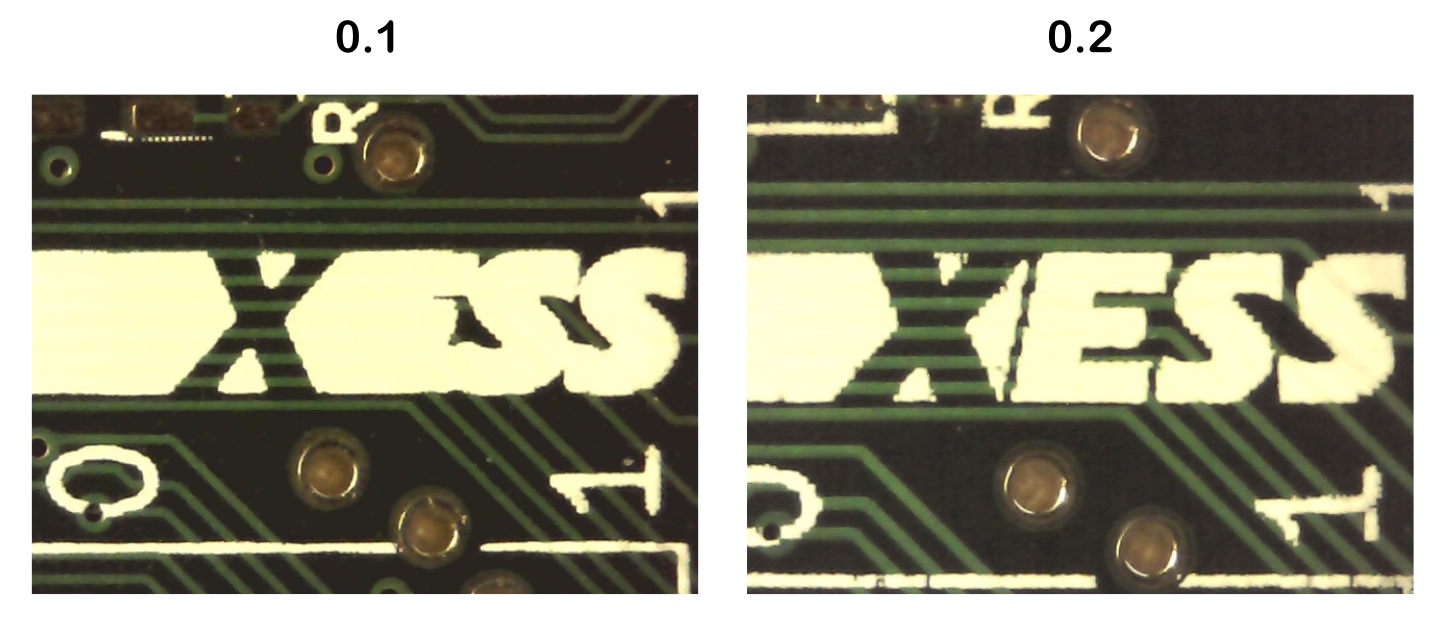
Looking a little more closely, the PCBCart silkscreen is better defined than the one by PCBWay which suffers from some "blooming". But that also makes the part references on the PCBCart PCB look a bit spidery so it's probably a good idea to thicken the text a bit for those.
![]()
Now let's look at drill/via alignment. The vast majority of the small 20-mil vias had drill holes punched completely within the copper pad. But there were a few vias in each set of boards that had "breakouts" like those shown below. Thankfully, there were no cases where the drill missed the via completely in either set. For this metric, the PCBWay boards were slightly superior to those from PCBCart but there were no outright failures in either.
![]()
The above image also shows the alignment of the soldermask with the BGA pads. Bad alignment can lead to BGA balls not connecting to the pad or having a ball short to a nearby, uncovered via pad. Neither of those is a good thing. The PCBWay boards have a bit more misalignment than those from PCBCart, but not as much overall as the image above would make you believe. Still, for this metric PCBCart has a slight edge.
Another factor to consider is via size. PCBWay can drill holes as small as 8 mils but they require a 6 mil annular pad so the total via diameter is 6 + 8 + 6 = 20 mils. PCBCart drills a larger 10 mil hole but they only need a 4 mil annular pad for a total via size of 18 mils. When you're putting vias between the pads of an 0.8mm BGA and then trying to squeeze traces between them, that extra 2-mil clearance is a big advantage. Of course, the smaller pad size will also lead to more of the drill breakouts we saw above.
Regarding price, I got 11 PCBs from PCBWay for $185 and 10 PCBs from PCBCart for $166. So the per-board price is about the same. But this changes all the time, so always check before submitting a board.
Now I'm on to building some CAT Boards using the new PCBCart PCBs. That will be the true test.
-
Back From Vacation (My PCBs, That Is)
04/14/2016 at 11:56 • 0 commentsMy wayward PCBs that were erroneously shipped to New Caledonia have arrived! PCBCart arranged to have them shipped to me in NC for no charge (to me; I'm not sure what it cost them). That was nice of them, since they were under no obligation to do that. So +1 for customer service!
![]()
-
What goes to New Caledonia, stays in New Caledonia...
04/04/2016 at 15:48 • 2 commentsI finished testing the major systems of the CAT Board about four weeks ago. Based on what I found, I made the following changes:
- Straightened out the MISO/MOSI mess between the FPGA, serial configuration flash, and the Raspberry Pi. Now the FPGA should be programmable from either the RPi (during development) or the flash (for dedicated applications).
- Added series resistors between the RPi SPI pins and the FPGA/flash chips to prevent any possible contention while still letting the RPi get control of the FPGA.
- Fixed the footprint for the SATA connectors which I first created in 2004 with Eagle and either didn't get right or it changed since then. (Of course, this required some adjustments to the layout since the new footprint is wider and the two connectors were already very close together.)
- Rerouted the SATA I/O lines from the FPGA in order to get 100-ohm differential impedances.
- Simplified the way the voltage is programmed for the adjustable VCCIO_3 bank of FPGA I/Os. (Now it's done just by changing a single resistor instead of using solder-bridge jumpers.)
I regenerated the gerber files and went looking for someone to fabricate them. I previously used PCBWay and they did a good job for $180, but 3 of the 11 boards they sent had enough soldermask misalignment to make me leery of using them. I had also considered PCBCart, but at the time their prices were considerably higher (around $230, as I recall). But when I went back and requoted them again, the cost had dropped to $167.
So I submitted the gerbers to PCBCart's online ordering system and waited. They fabricated the PCB in a week and shipped it ... to New Caledonia! Now you may not know where New Caledonia is (I know I didn't), but it's best described as "the ass-end of nowhere": hundreds of miles off the east coast of Australia in the middle of the South Pacific. The only way to get farther from North Carolina in the USA would be to ship to Samoa (which, I guess, makes that "the colon-end of nowhere".)
This screwup was caused by some interaction between the automatic address fill-in feature of Google Chrome and the PCBCart web forms, and by me not checking the PCBCart status emails closely. PCBCart got my billing address mostly correct, but the shipping address was completely whacked and I never noticed.
So my CAT Board PCBs currently sit in New Caledonia, enjoying the onset of Fall in the Southern Hemisphere. DHL will tranship them from there to me for $163. What I'm hoping is that the shipment will be undeliverable and DHL will return it to PCBCart who can then send it to me for less than that.
We'll see.
-
CAT Board SDRAM Test
02/25/2016 at 19:02 • 1 commentIt's been a while. I got the SDRAM on the CAT Board working a few weeks back, so I'll use this post to document that.
I've been using SDRAMs with FPGAs since 2001. Back then, I created an SDRAM controller module in VHDL that manages all the SDRAM timing, bank and row activation, address multiplexing and refreshing while presenting an interface that looks like a static RAM to the rest of the FPGA.
To test an SDRAM, I attach the controller to a finite state machine (FSM) that sequences through a two-phase process:
- Write the entire SDRAM with a pseudo-random sequence from a random number generator (RNG).
- Reinitialize the RNG with the same seed and then compare its output to the values read from the SDRAM. If the outputs from the RNG and SDRAM match over the entire address range, then the test is passed.
Since I've switched to using MyHDL for the CAT Board, I needed to convert the SDRAM controller. That's a big job. Luckily, I mentored a student for the 2015 Google Summer of Code (GSOC) and he translated the controller to MyHDL. He also provided a simulation model of the SDRAM chip.
Converting my RNG into MyHDL should have been a much simpler task. At least, it would have been if I was the kind of guy that didn't go to extremes. As it was, I created a Jupyter notebook that simulates several versions of RNGs with MyHDL and visualizes the probability distributions they output. All that to end up with a standard LFSR-based RNG.
I combined the MyHDL modules for the SDRAM, SDRAM controller, RNG and FSM and simulated the entire test process. The simulation found a small bug in the SDRAM controller that was the cause of a failure in one of the GSOC tests during the summer. (So *that's* what caused it!)
Once the simulation was working, I tried to map it to the FPGA on the CAT Board. Unfortunately, the SDRAM controller describes its I/O using interfaces instead of lists of signals. Interfaces are a (relatively) new MyHDL feature that simplifies the interconnection of modules and reduce errors (that's good!), but using them with pin assignments is undocumented (that's bad!). So I had no way to assign the individual I/O signals to the FPGA pins connected to the SDRAM on the CAT Board.
I finally resorted to exporting a Verilog version of my design using the MyHDL conversion routines. Using the port definitions in the converted Verilog code, I made the appropriate pin assignments for the CAT Board within Lattice's iCEcube2 software. Then I compiled the Verilog using the iCE40HX8K FPGA as the target device. I took the bitstream generated by iCEcube2 and transferred it to my Raspberry Pi.
From there, it was just a matter of having the RPi download the bitstream to the FPGA on the CAT Board and running the SDRAM test. Here's what happened:
So the SDRAM works! That was actually a little easier than any of my previous tests.
-
The Travails of Using GPCLK0
12/02/2015 at 05:27 • 4 commentsThe CAT Board has a 100 MHz Si501 MEMS oscillator on board, but the iCE40 FPGA can also be clocked from the GPCLK0 pin on the Raspberry Pi GPIO header. All I had to do was enable that clock and program the output frequency.
I started off with RPi.GPIO. I modified a simple Python program I found here to get this:
import RPi.GPIO as GPIO

GPIO.setmode(GPIO.BCM)
#set the alternate mode for pin 4 (GPCLK0)
GPIO.setup(4,GPIO.ALT0)
#set the clock frequency to 64 Khz)
GPIO.setclock(4,64000)
#turn on the clock
GPIO.output(4,1)
But when I ran it, it complained that GPIO.ALT0 was undefined. Sure enough, a little poking around in IDLE showed ALT0 was non-existent. One of the commenters in this thread from 2015 verified that none of the ALTx codes were supported in the current version of RPi.GPIO. I guess the code I modified came from a few years earlier.So I got hold of the WiringPi library with its gpio command-line tool. I could (supposedly) put the GPCLK0 pin into the ALT0 mode using the command:
gpio -g mode 15 alt0That seemed to do something to the GPCLK0 pin: it went from a 3.3V to ground.Next, I ran my Python script with the GPIO.setup(4, GPIO.ALT0) disabled. Unfortunately, I got another error message that the setclock routine was undefined. At this point, I abandoned RPi.GPIO.
I looked through the WiringPi documentation but didn't find any facilities for working with the GPCLKx pins. So I abandoned that, too.
I found mention of a small program for getting a 10 MHz clock out of the GPCLK0 pin. After downloading and compiling the source code, the program would execute but stalled in a loop waiting for the clock pin's busy flag to go active. So that was a bust.
Most of the code I found that handles GPCLK0 seems to be from a few years ago and probably worked with the BCM2835 in the original Raspberry Pi B/B+. I have the RPi 2 that uses the BCM2836, so the register addresses and bit positions have probably changed enough to render the old code useless.
So I need to look further on how to unlock the power of the GPCLK0 pin. Thankfully I placed that 100 MHz oscillator on the CAT Board or else I would have been really stuck.
Of course, on top of all this, the Si501 chip was discontinued a few months ago...
-
"That's Going to be SO EASY!"
11/30/2015 at 15:12 • 2 commentsAfter struggling to get the tristate drivers working for the LED digit array, I decided I needed to test something nice and easy: the CAT Board DIP switches and push buttons. I would just display the hexadecimal digit for the four-bit DIP switch on the LED digits and then turn it on-and-off using the momentary pushbuttons. Simple!
The only part I was unsure about was enabling the built-in pullup resistors on the input pins of the iCE40 FPGA attached to the switches and buttons. (I use these so I don't need discrete pullups on the board, which saves PCB area and money for parts and assembly). But I looked in the source for some of the auxiliary MyHDL tools, and it appeared something like this could be used to turn on the pullups:
brd.add_port("gpio", pins=(23,24,25,26,), PULLUP='PULLUP')So I wrote a bit of MyHDL code for the buttons+switches+LED test, compiled it, downloaded it to the CAT Board, and ... nothing. The LED digits displayed "0" no matter how I set the DIP switches, and the display never changed when I pressed the pushbuttons.Probing the pins with an oscilloscope showed they were always at ground, so the pullups didn't look like they were enabled. I looked in the pin constraints file that was generated from my MyHDL code and the correct pin assignments were in there, but there was nothing about turning on the pullups. So I looked in the Verilog code that had been generated and it didn't have anything about the pullups either. Then I examined the code for the MyHDL converter and saw that it only processed the pin assignments and ignored everything else. So there's the problem.
To make some progress, I decided to add the pullup enables directly to the pin constraints file. I wasn't exactly sure of the syntax for doing that so I just added the string from the MyHDL code. The yosys Verilog synthesizer would probably throw an error when it saw that, but I could use that to track down the place in the code that handles pullups and get the correct syntax from there.
Surprisingly, yosys didn't complain when I ran it with the altered constraints file. But the new bitstream showed the same erroneous behavior when I downloaded it to the FPGA, so I still hadn't fixed the pullup problem.
If yosys was ignoring the pullup constraint, my next line of attack was to enter the constraint into the BLIF file that was generated and passed to the arachne-pnr place-and-route tool. As explained in this blog post, you can enable the pullup on an iCE40 FPGA input pin by changing the parameters for the associated SB_IO block. Unfortunately, when I looked into the BLIF file for my test circuit, there were no SB_IO blocks in it.
I was well-and-truly stuck, so I emailed Clifford Wolf and asked how I could use pullups with yosys. He replied that you currently had to instantiate them directly like this:
	module top(inout pin);
		wire outen, dout, din;

		SB_IO #(
			.PIN_TYPE(6'b 1010_01),
			.PULLUP(1'b 1)
		) io_pin (
			.PACKAGE_PIN(pin),
			.OUTPUT_ENABLE(outen),
			.D_OUT_0(dout),
			.D_IN_0(din)
		);
	endmodule
Now all I had to do was figure out how to do that in MyHDL, but it turns out it's already supported using user-defined code sections. All I had to do was define an input_pin module consisting of:- a Python routine that describes how the input pin behaves during simulation, and
- a string of Verilog code that is inserted for the pin during the conversion process.
from myhdl import *

inst_num = 0

def input_pin(i, o, pullup=False):
    global inst_num
    inst_num += 1

    array = ''
    if len(i) > 1:
        array = '[{}:{}]'.format(len(i)-1, 0)

    pup = 0
    if pullup != False:
        pup = 1

    @always_comb
    def in_to_out():
        o.next = i

input_pin.verilog_code = \
"""
SB_IO
#(
    .PIN_TYPE(6'b000001),
    .PULLUP(1'b$pup)
) input_with_pullup_$inst_num $array (
    .PACKAGE_PIN($i),
    .D_IN_0($o)
);
"""
But after modifying my design to use the input_pin module, the MyHDL Verilog converter complained about unused input pins and undriven internal signals related to the switches and buttons. These errors occur because input_pin.verilog_code is just a text string so the converter can't interpret what the inputs and outputs of the SB_IO module are and whether they are used or not. It turns out I missed a crucial bit of the documentation and omitted the following lines from the Python routine:def input_pin(i, o, pullup=False): global inst_num inst_num += 1 array = '' if len(i) > 1: array = '[{}:{}]'.format(len(i)-1, 0) pup = 0 if pullup != False: pup = 1 @always_comb def in_to_out(): o.next = i o.driven = True # Tell converter this output is driven! i.driven = True # Tell converter this input is used!That was the final piece of the puzzle: now my design compiles and works correctly on the CAT Board. Here's a short video of the results from this long process:
-
Driving an Array of LED Digits with the CAT Board
11/03/2015 at 06:48 • 8 commentsWow, it's been almost two weeks since I posted! I've been through hell and back.
After getting the simple LED blinker working with the open-source myhdl+yosys+arachne-pnr toolflow, I decided to take one of my existing designs and port it to the CAT Board. I chose the driver interface for the StickIt! LED digits board because I could attach that directly to one of the PMOD sockets on the CAT Board for testing purposes.
The driver uses eight tristateable outputs to control eight seven-segment LED digits. Forcing a high level on one of the outputs powers the common anode of one of the digits. Driving a low level on one or more of the other seven outputs will pull down the cathodes associated with those segments so current will flow and make them light up. The drivers for the rest of the segments are placed in the high impedance state so no current flows and the segments stay dark. Meanwhile, all the other digits stay completely dark because their anodes are either pulled to ground or in a high impedance state. After the pattern on the first digit is displayed, the next digit is activated by powering its anode and placing a pattern of low levels and high impedances on the other seven outputs. A stable pattern of eight characters is displayed by repeatedly cycling through all the digits.
The first challenge was to recast my VHDL code for the LED driver into MyHDL. I had an academic understanding of MyHDL, but that's quite different from actually constructing something that compiles, simulates and synthesizes into an FPGA. Obviously the syntax of MyHDL is different from VHDL, but you also have to re-learn how a design should be organized and partitioned for a new language.
One of the challenges I faced was the heavy use of tristate outputs in the design. MyHDL supports tristate buses, but it doesn't allow bits within a bus to be individually tristated. So I had to break the eight-bit LED driver bus into eight individual signals, which made it more cumbersome to handle since loops couldn't be used.
The MyHDL compiler converts MyHDL source code into Verilog or VHDL that is passed to the synthesis tools for a particular FPGA. But I found the Verilog and VHDL code for the tristate outputs wasn't actually connecting them to the internal logic in the driver. This problem was eventually resolved by attaching each tristate port to a dummy signal inside the driver code so that the port looked more like a true I/O port. It was easiest to implement this fix by building a separate tristate module and instantiating it eight times, once for each output. More cumbersome code.
I attempted to clean the code and make it more parameterized by refactoring it to use loops. While this worked in simulation, and was convertible into Verilog, the yosys synthesizer choked on it because it was, in fact, not synthesizable. So I had to remove the loops and use a more "unrolled" coding style. More cumbersome code.
Finally, I designed some code to send inputs to the LED driver and display a pattern of eight characters. Unfortunately, using an array of byte-wide signal vectors for the characters led to some strange errors. Instead, I had to use a single 64-bit vector with each eight-bit field representing a character to get the behavior I wanted.
After all was said and done, I finally got the LED driver to work:
-
Open Source Tool Flow Works!
10/21/2015 at 04:43 • 1 commentI actually got the open source FPGA tools working on the RPi a few days ago, but I've been remiss in posting to this log.
Ed Vidal provided me with an archive that I could load onto my RPi using the squashfs tools. Unfortunately, they didn't work. It turned out I was running the Raspbian Wheezy distribution and I had to upgrade to Jessie. After doing that, it was easy to compile a simple blinker example. (Ed even prepared the example with the correct pin assignments for the CAT Board. What a guy!) Then it was just a matter of downloading the bitstream to the CAT Board and watching the LEDs turn on and off. Check out the video below for all the excitement!
With the RPi-host FPGA tools in place, example designs can now be compiled to test the SDRAM and I/O ports.
-
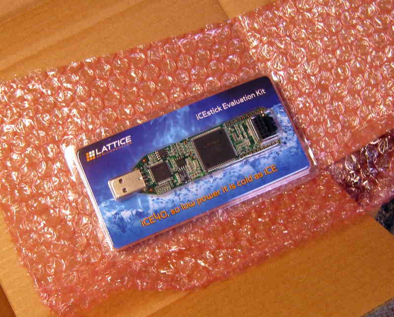
A Day Late and a Dollar Short
10/17/2015 at 15:26 • 6 commentsYou know how in action movies the cops always arrive after the bad guy has been taken out? Well, the Lattice iCEstick I ordered arrived today.
![]()
Since the CAT Board is working (at least the bitstream configuration part), I'll probably hold on to the iCEstick for a week and then send it back if I don't find any new problems.
I know, you're probably thinking "It's only $20. You'll use it for something!" Well, no, I won't. I've got half a dozen dev boards sitting around that have never been used (and I'm not alone in that). It's time to break the addiction before I end up on "Hoarders".
CAT Board
The CAT Board is part of a Raspberry Pi-based hand-held FPGA programming system.