David Scholten
-
It's Still Too Damn Hot!
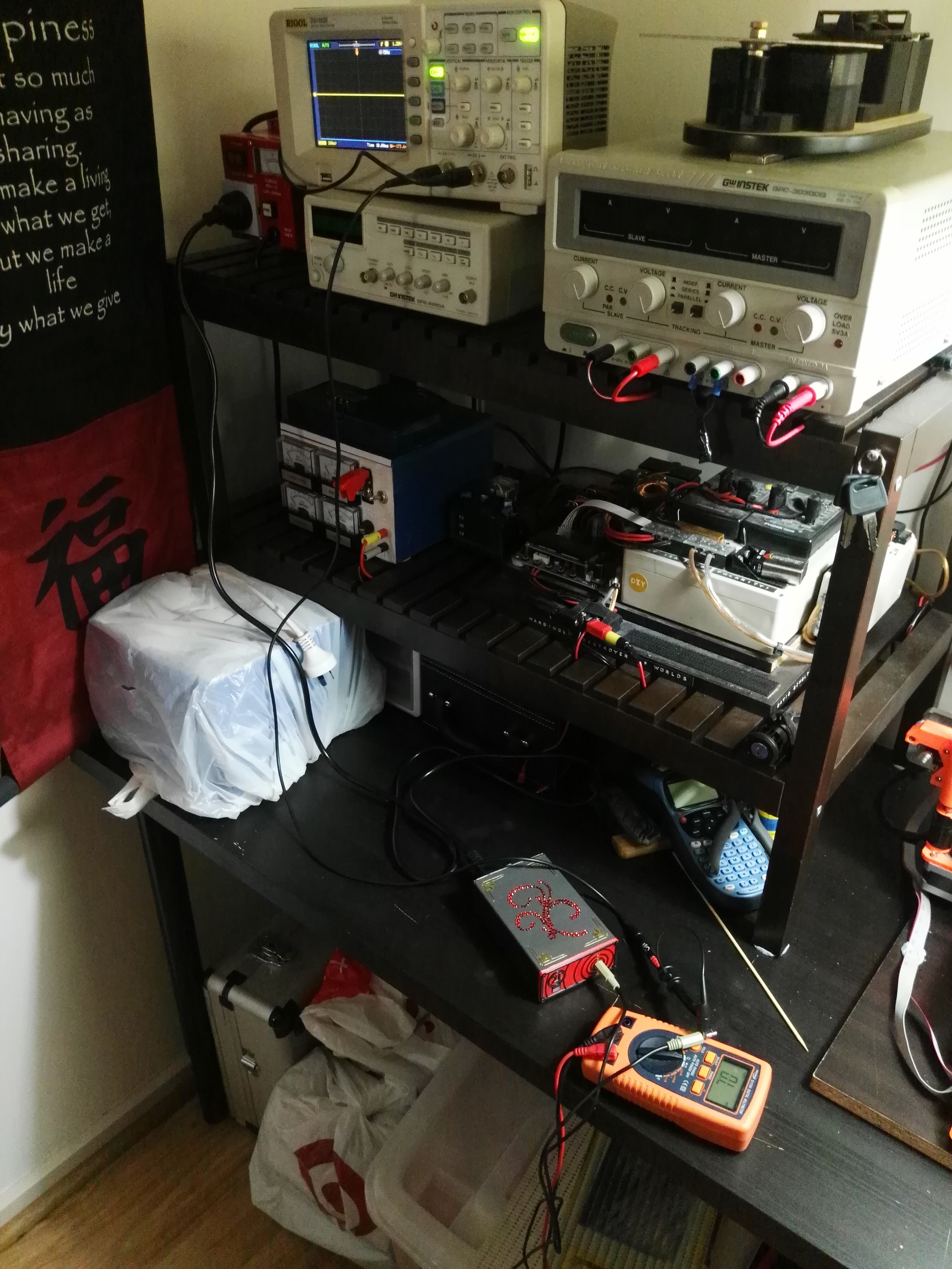
10/20/2018 at 12:42 • 0 commentsOkay, after leaving it running for 3 hours with a thermocouple in it and the "grid" (variac) set to 280Vrms I've found the following:
-->The air temperature just above the transformers reaches about 65 degrees Celsius
-->Laser gunning the metal-can electrolytics reveals they are at about 75-77 degrees Celsius (which we can approximate as the PCB temperature).
-->The temperature was still rising even towards the end of the test.This is what I can do to 70 degree Celsius PLA material with one hand by the way:
![]()
So, I know that the PCB is it's not convecting effectively enough (or likely at all) in the new case. However, I also know that the heat build up is so slow that ANY air movement will cool the thing down.
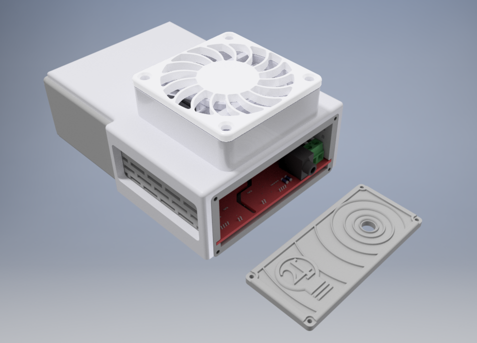
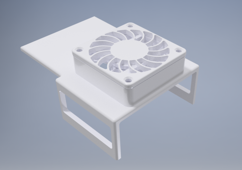
Well, then aside from ice cubes, air-conditioners and desk fans, this has to happen:
![]()
![]()
![]()
It's basically an add-on case assembly that clicks on top and adds active cooling to the device. It uses a 60mm 5V USB fan that will simply plug into the computer that is measuring it's output. In this way, the power is being drawn through the existing computer an is not utilising a potentially noisy additional power supply that would have been connected to the same power outlet as the Grid-2-Audio measurement device. However, I am still very concerned about induced EMI noise from the fan itself. We'll see how that goes soon:
![]()
-
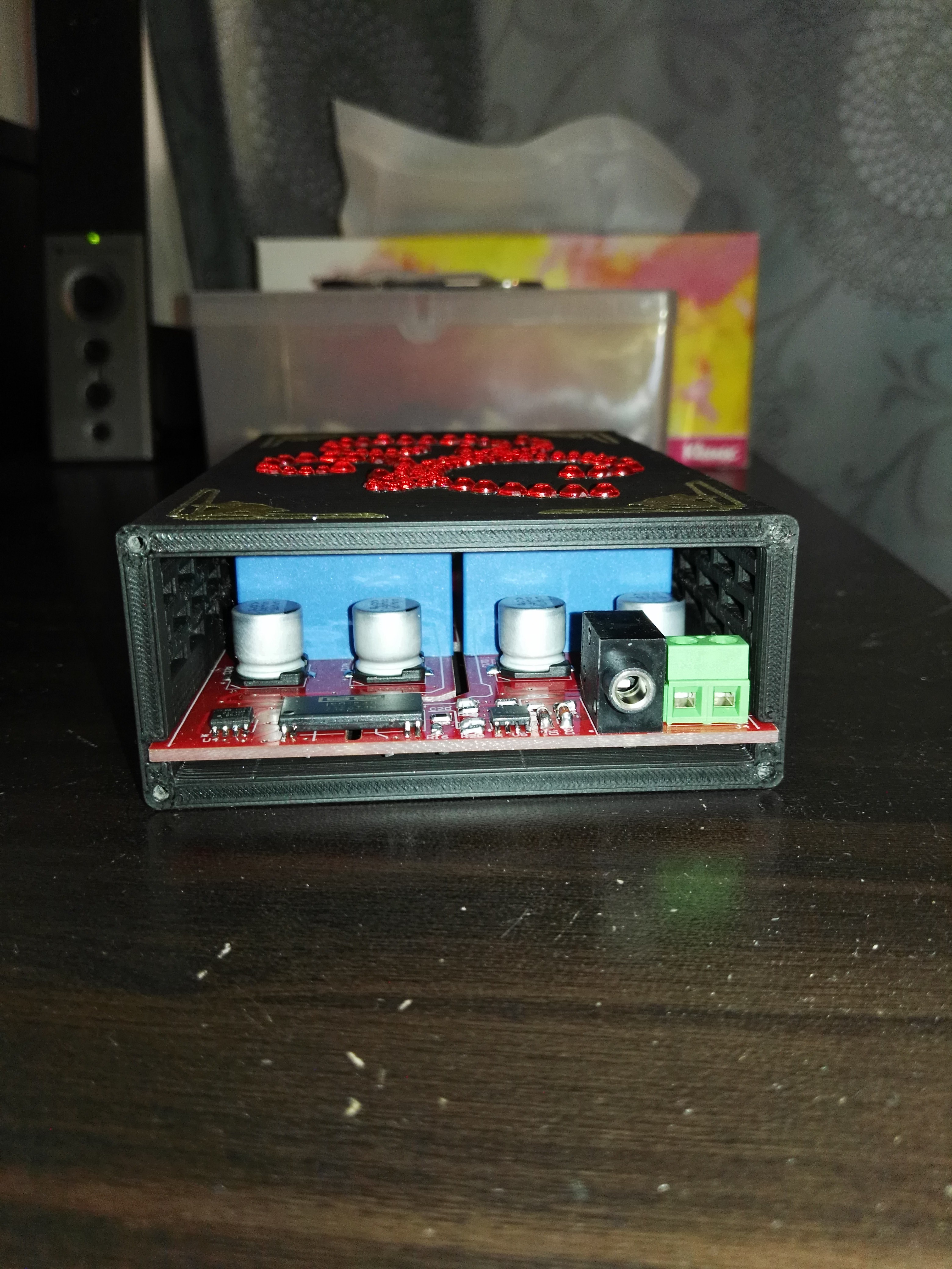
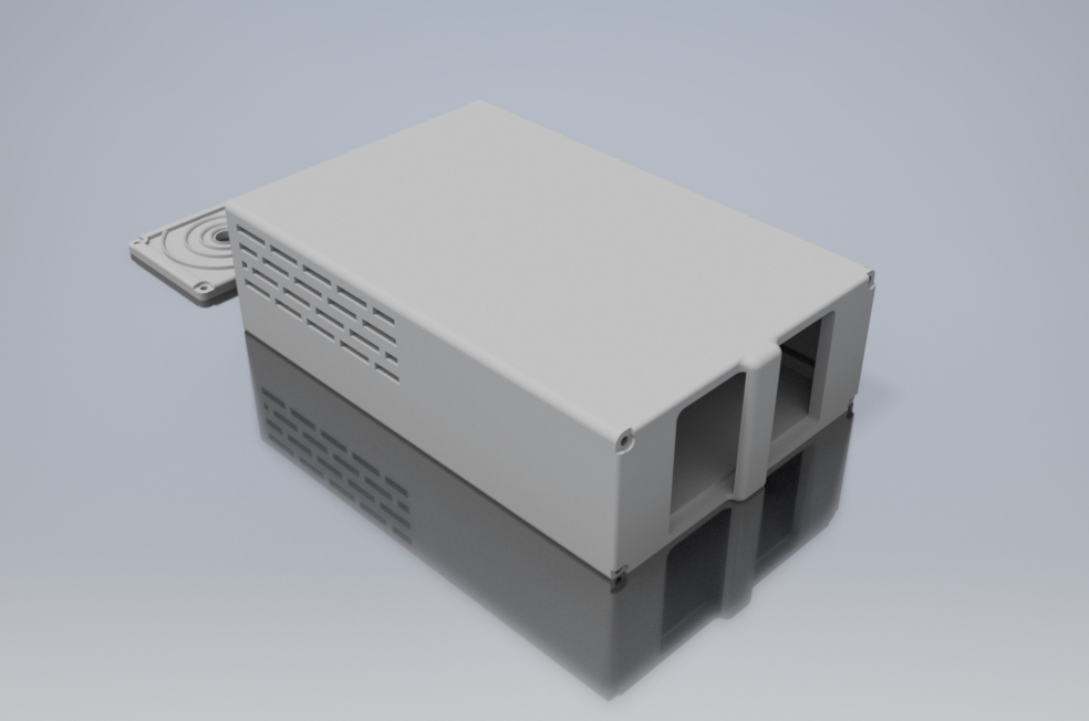
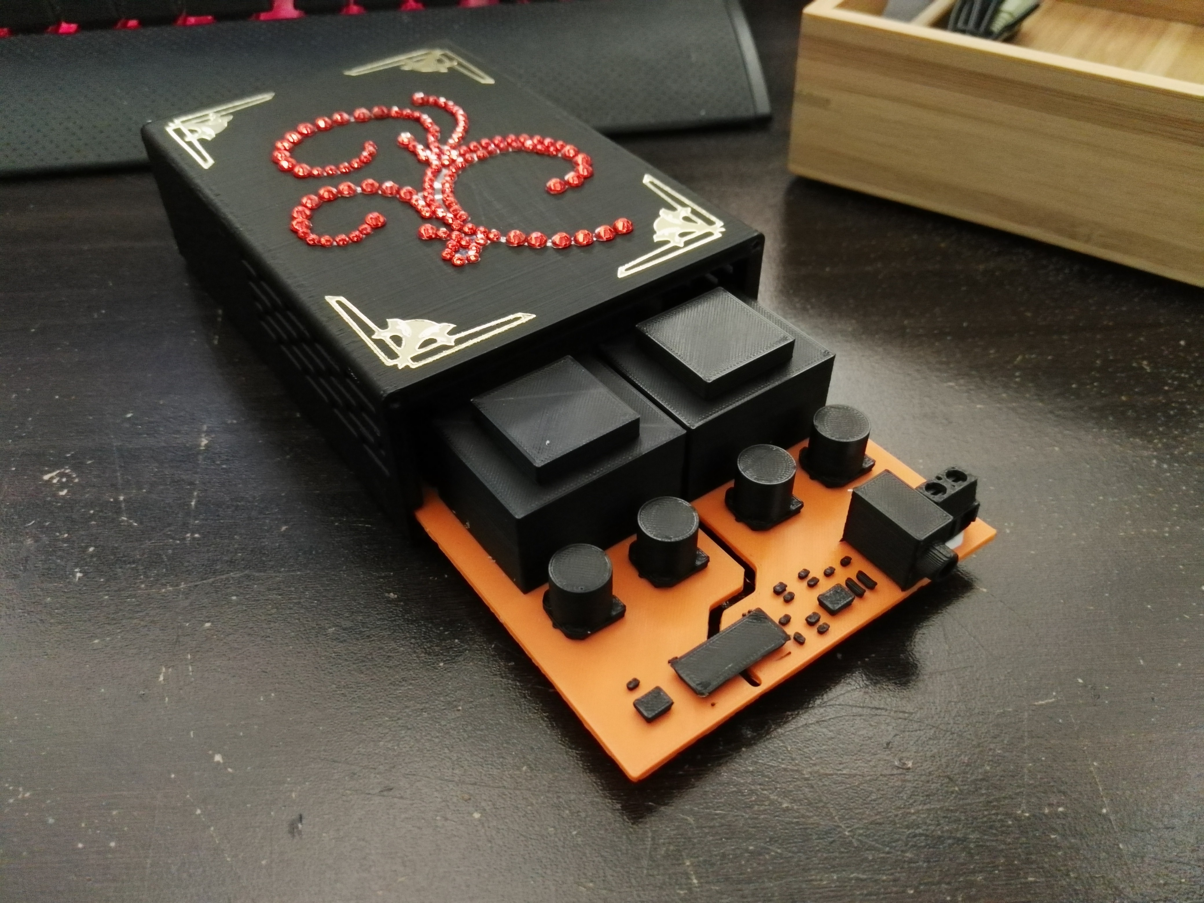
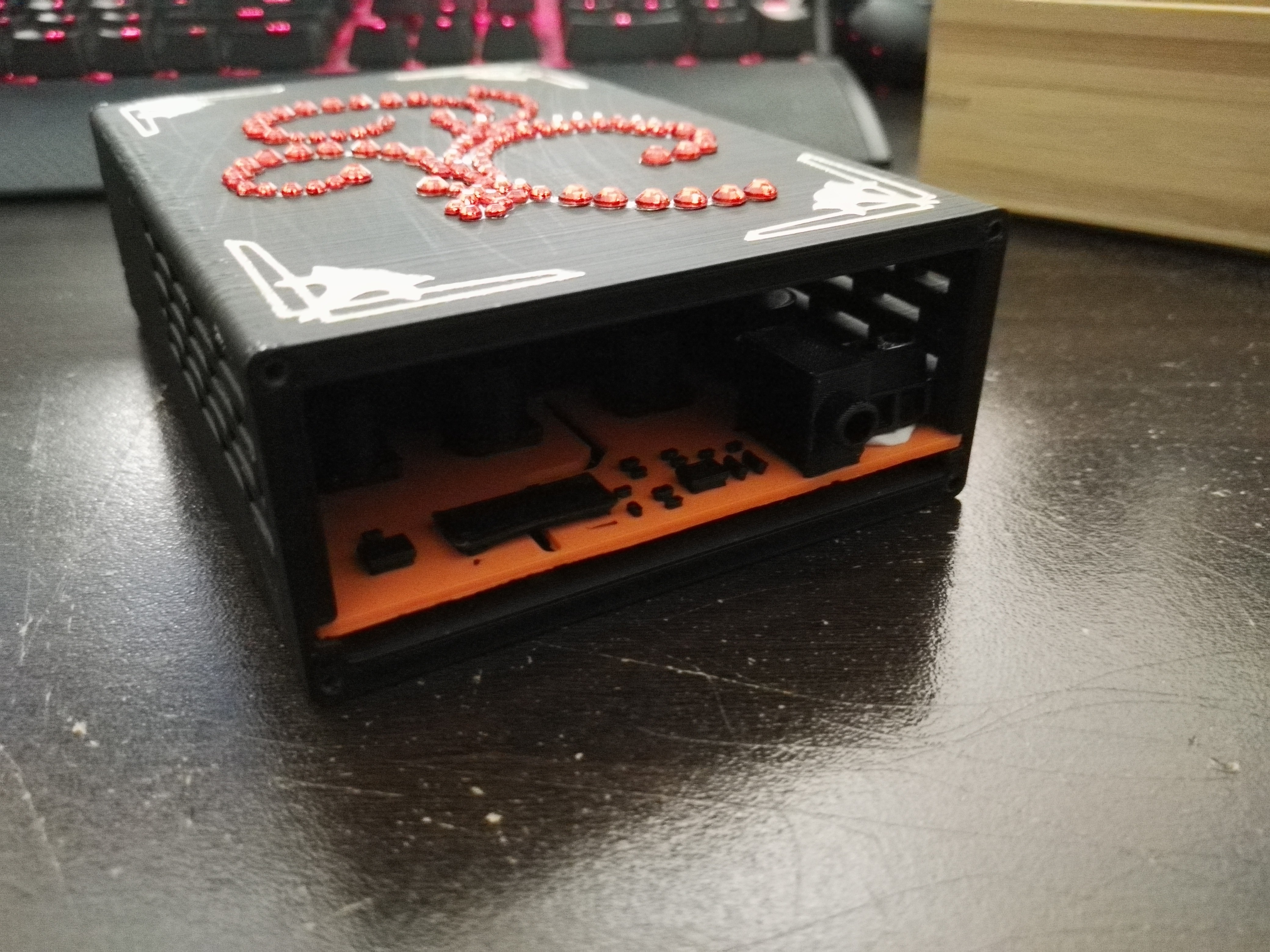
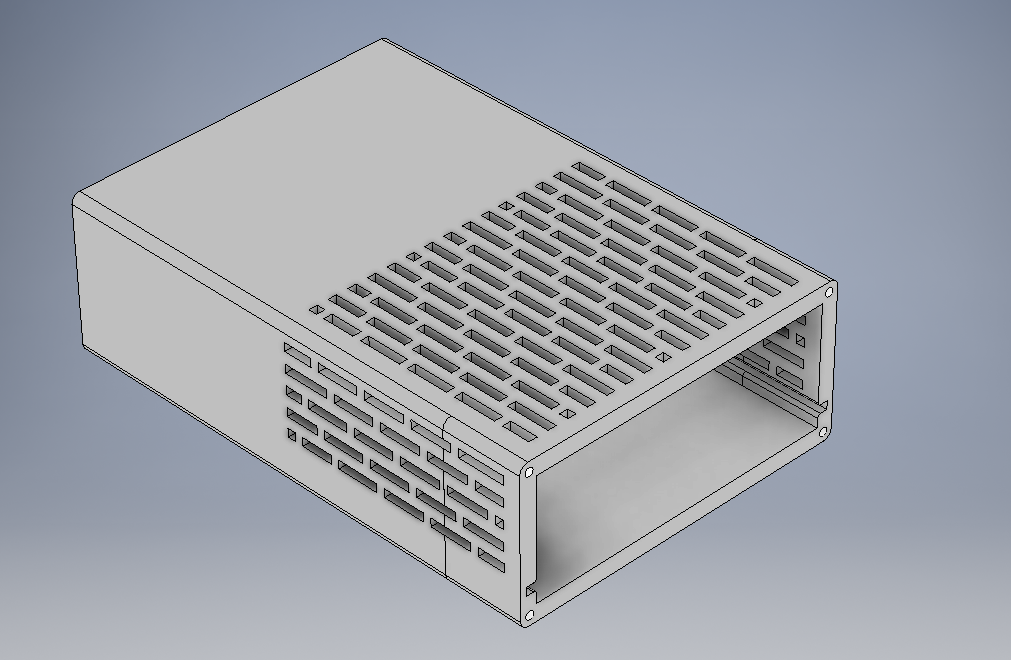
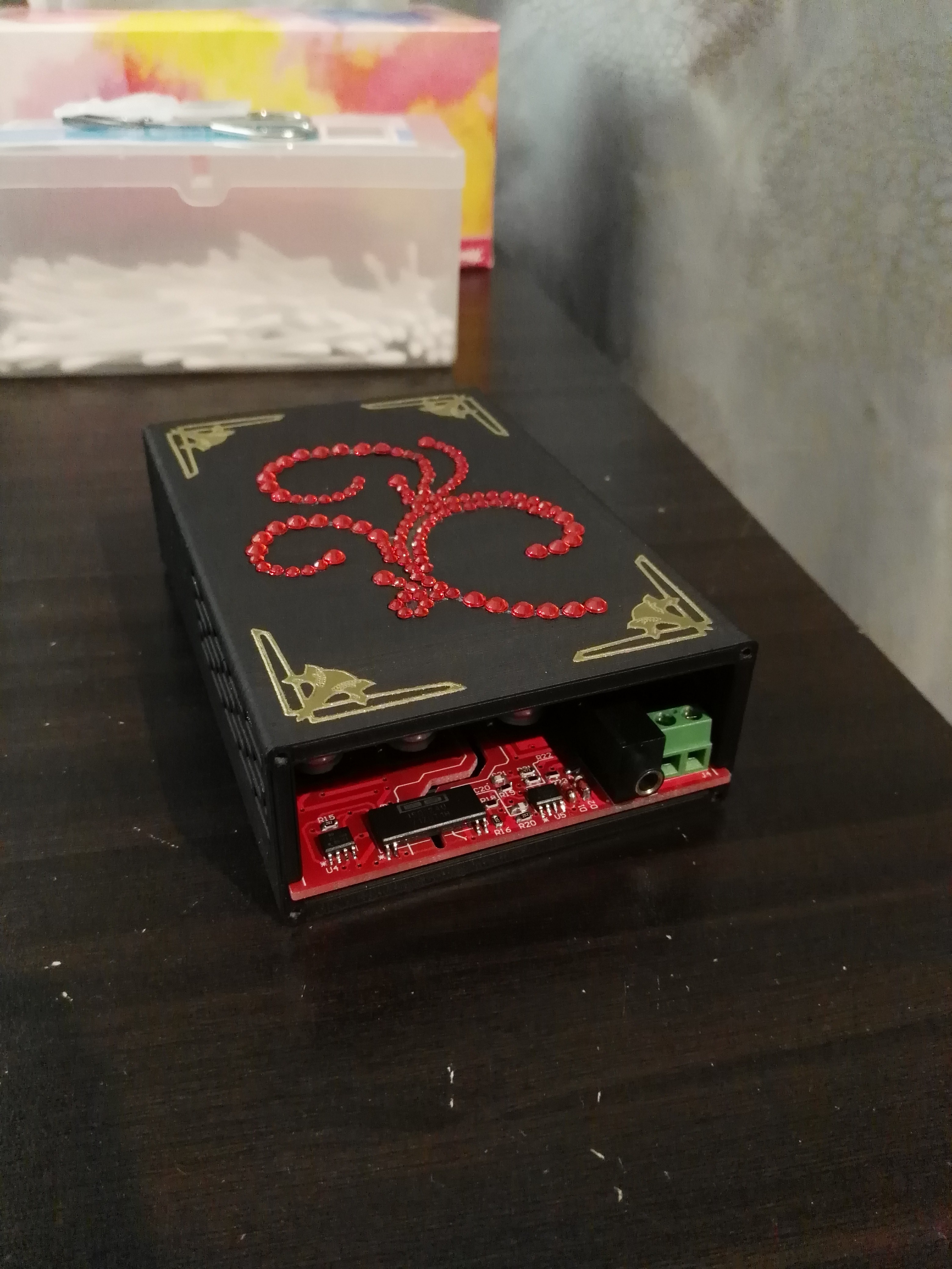
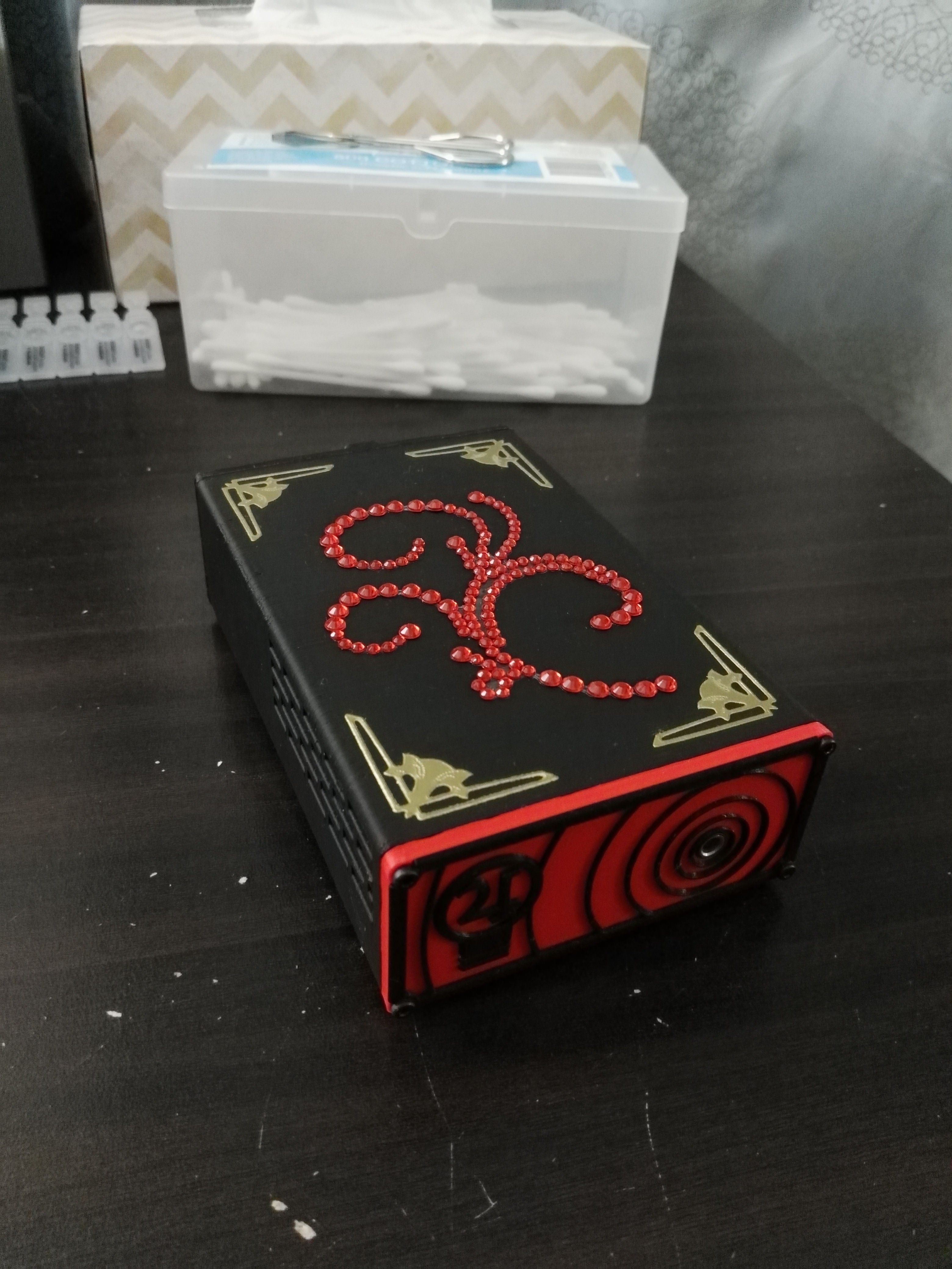
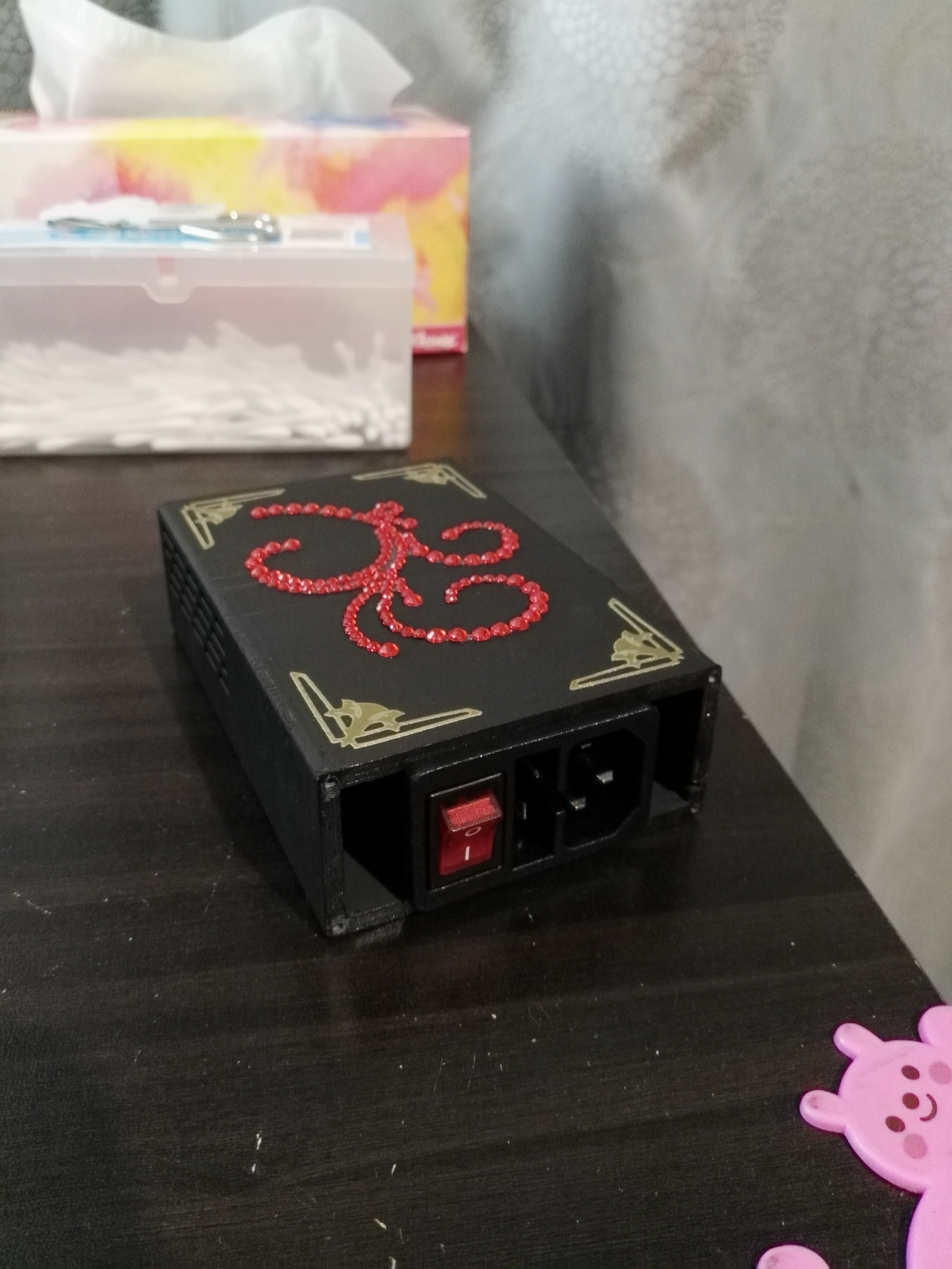
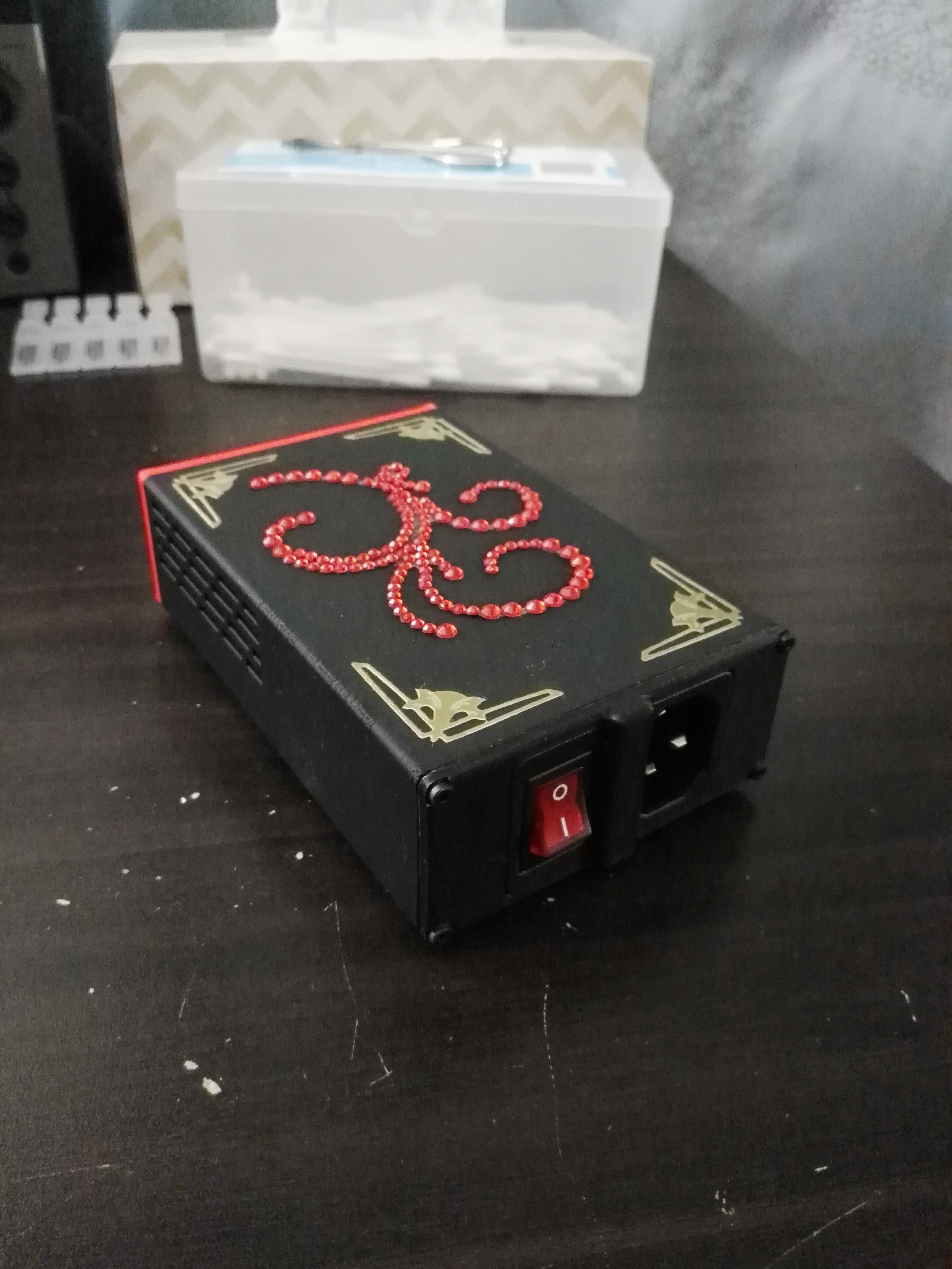
New Enclosure Finished
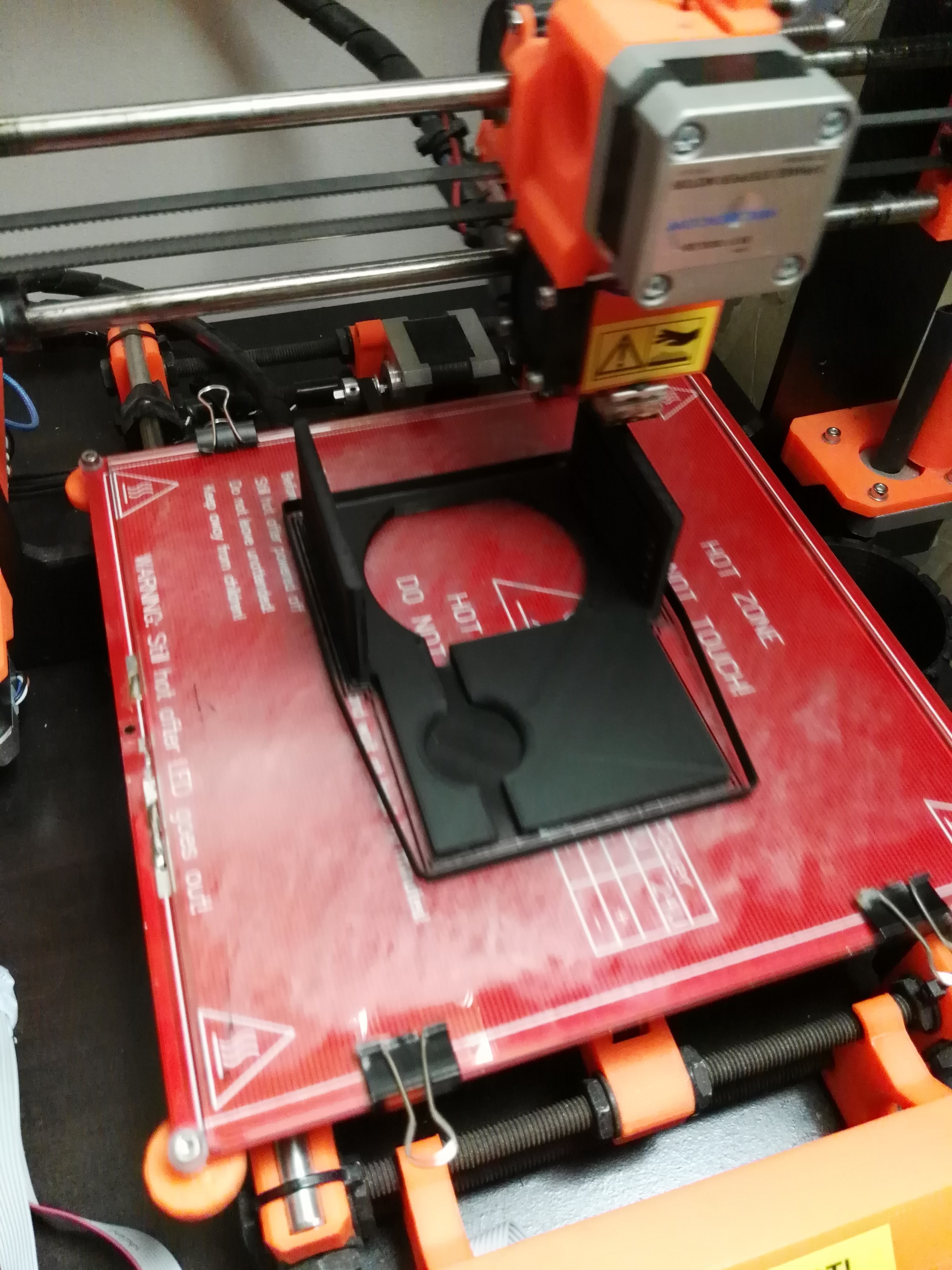
10/15/2018 at 12:14 • 0 commentsHere it is, the new enclosure fresh from the printer:
![]()
This was printed at a 100% percent infill with a 200um layer height and took 10 hours with a print speed of about 60mm/s. Not seen are the 5 rows of vents on the side of the unit, which should allow the air to flow in and to naturally convect upwards through the top vents.
Taking some measurements with the IR gun, the temperature of the bottom seems to reach 60 degrees Celsius on a fair day. It's a bit too hot for my liking, but there isn't anything else I can do and still maintain the safety of the device - Unless of course I give active cooling a go, but this would need an external power supply. Ultimately though, it should be fine, but with a side of caution.
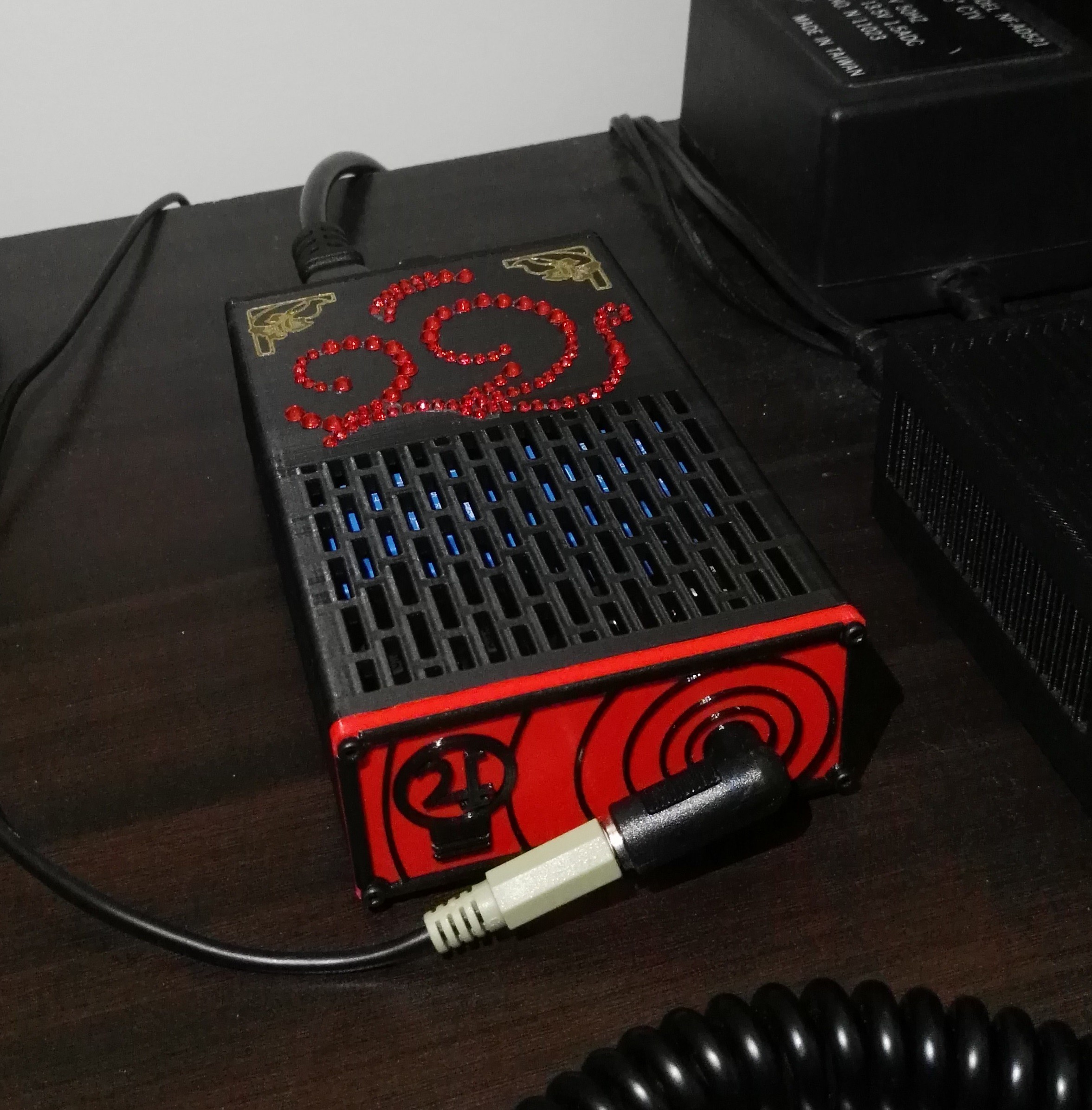
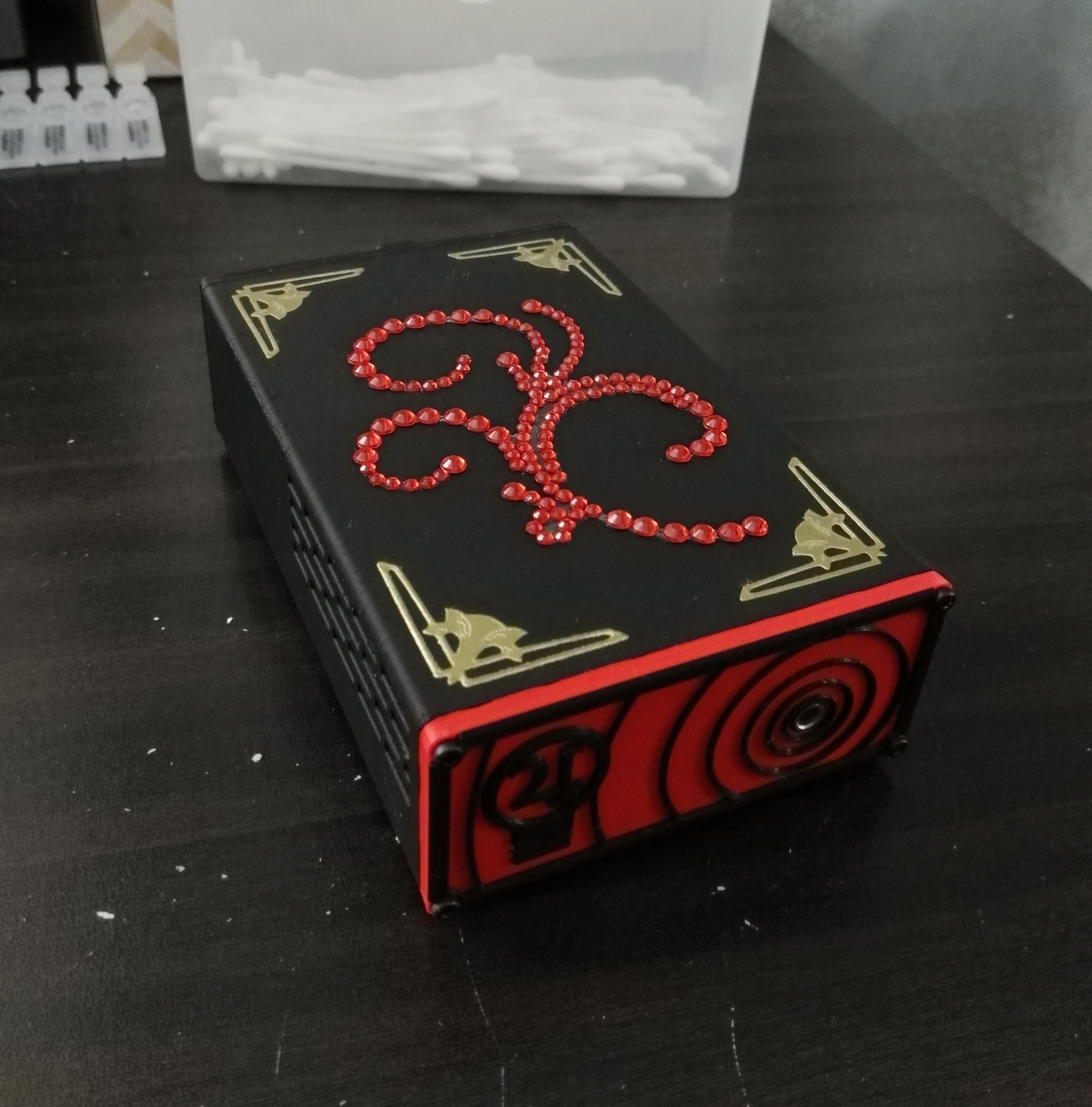
That aside, I did have fun decorating with the spare jewel thingies and stickers!
For comparison, here is the old casing:![]()
-
Some Basic Results
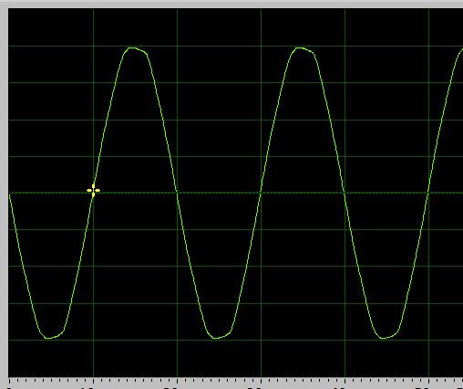
10/13/2018 at 12:29 • 0 commentsHere we have a waveform:
![]() And a spectrograph:
And a spectrograph:![]()
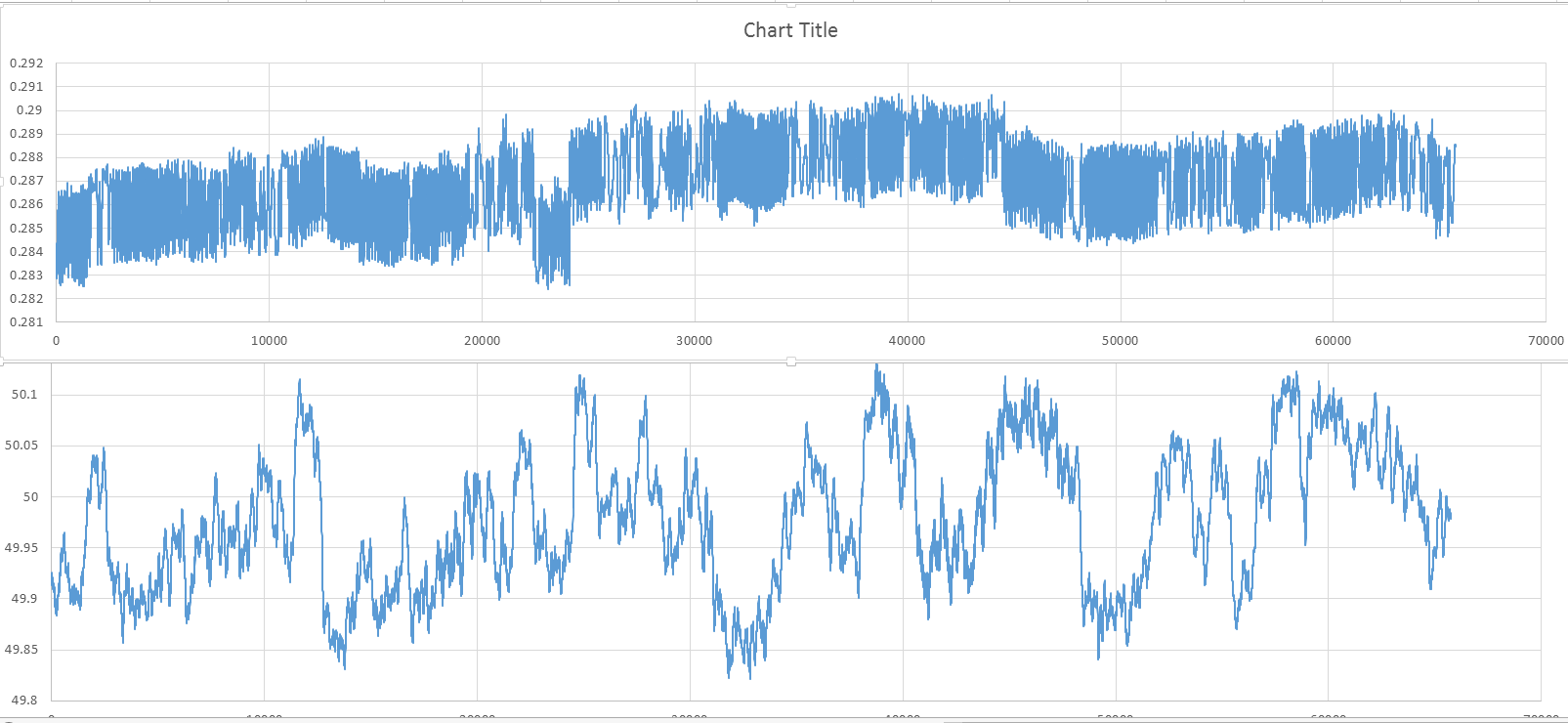
Finally, a plot of the RMS voltage (ignore the magnitude) at the top and the frequency at the bottom:![]() This was taken over a two hour period (8:10pm - 10.00pm) on a Saturday night in Adelaide. Although the voltage magnitude is nonsensical, the proportional values are very relevant. The frequency plot, however, is correct is it's measurements.
This was taken over a two hour period (8:10pm - 10.00pm) on a Saturday night in Adelaide. Although the voltage magnitude is nonsensical, the proportional values are very relevant. The frequency plot, however, is correct is it's measurements.
We can start to see some patterns emerging, such as a some sort of overall frequency governing control loop that operates with an approximate 49.9-50.1Hz hysteresis range across the network. This may just be a coincidence. Another theory is that as these dips seem to occur in half-hour intervals, which would coincide with the starts and stops of TV programming. I'll need to do a longer run and check the TV guide for what's on. Next I need to print the new case that will allow the board to run cooler - It heated up significantly during this run and I wouldn't leave it unattended at this point.
The 12 hour print starts tomorrow morning! -
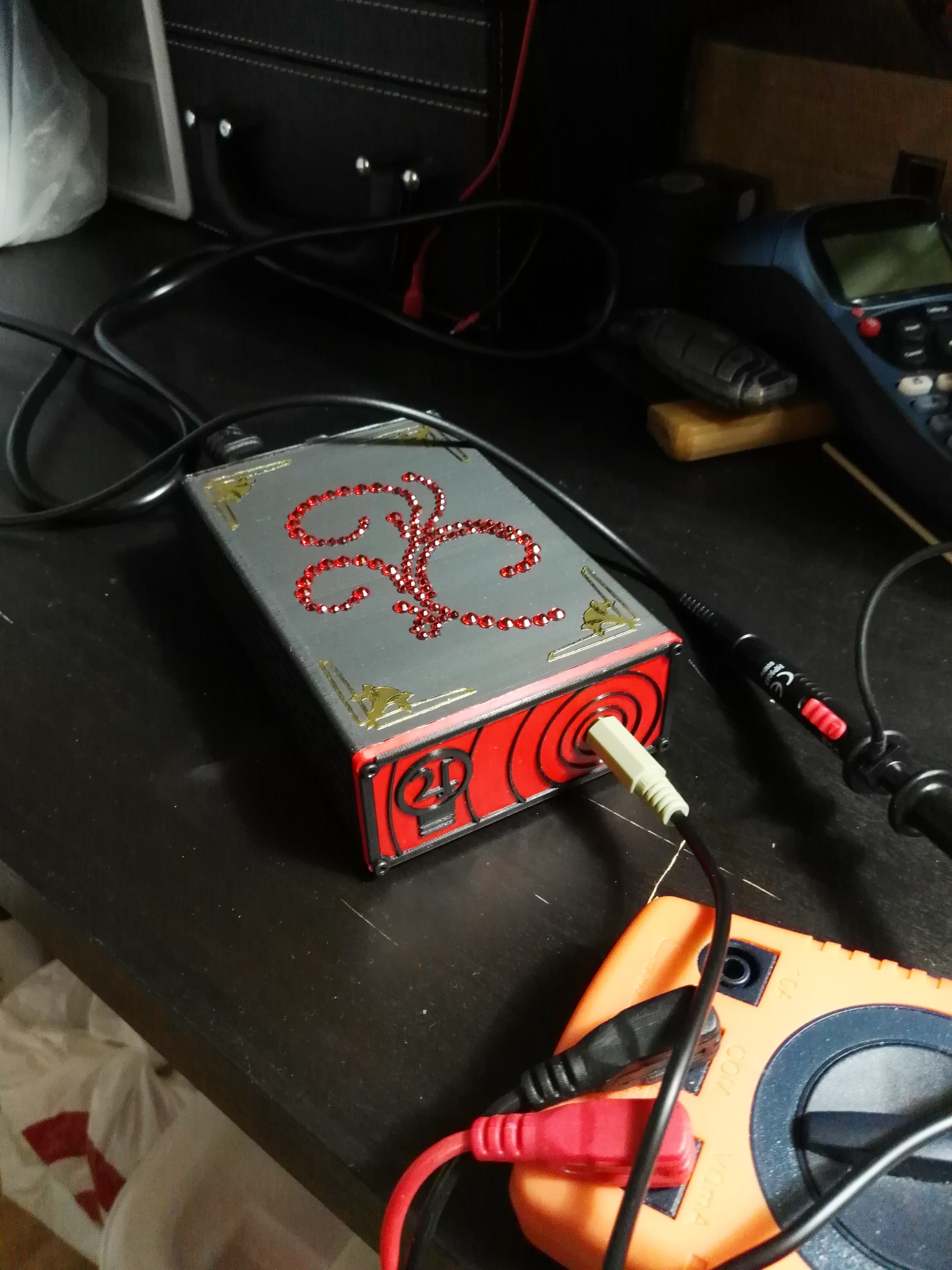
Hardware is Working! Waveforms be Soon!
10/11/2018 at 12:20 • 0 commentsYes! The hardware is finally working!
And of course, there were a couple of problems along the way.
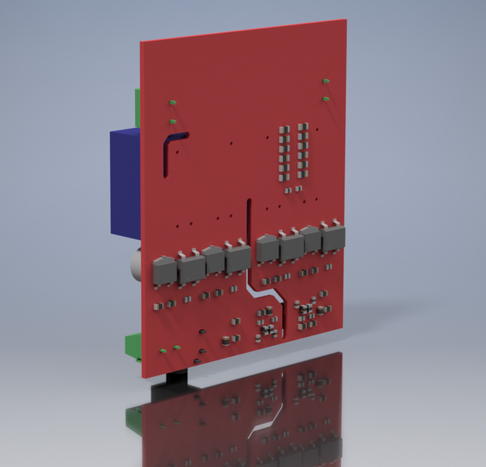
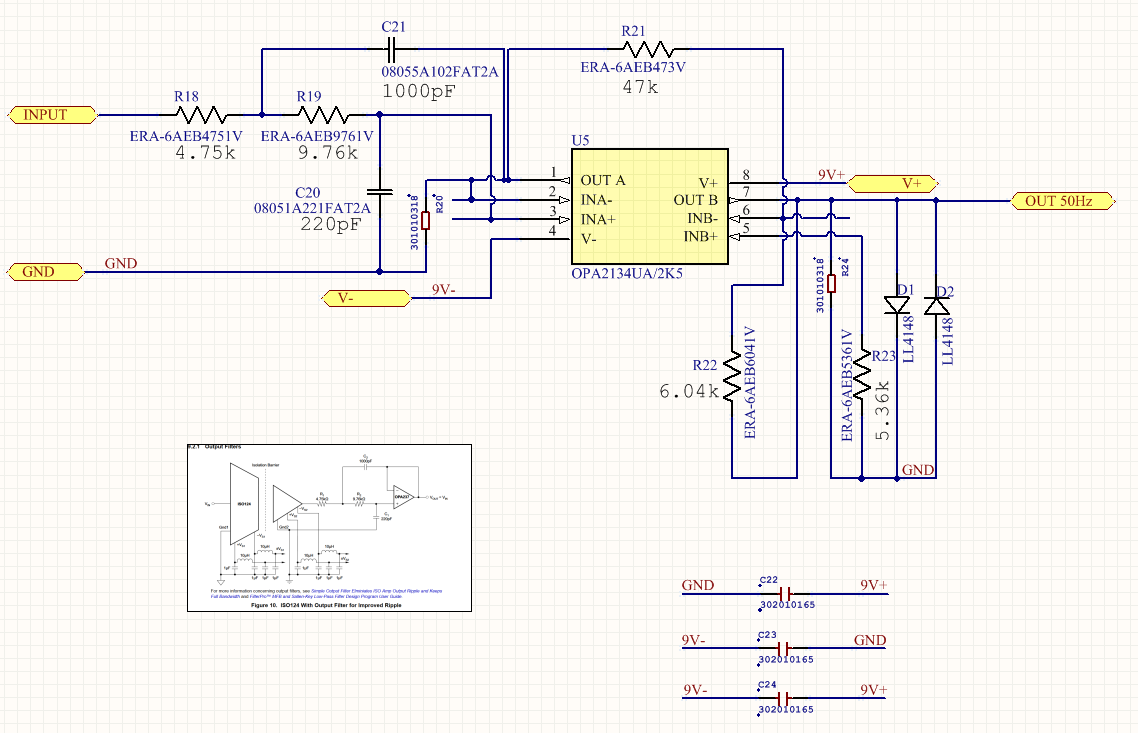
The first problem was an oscillating opamp (1.5MHz) right at the end of the signal chain. During the design I decided to remove the filtering capacitor across the inverting opamp's feedback resistor as I didn't want anything more than a 0.2% decrease of the 20kHz response. However, I didn't expect the opamp to completely take off in the way it did. To correct this a ~25pF was soldered to the top of R22 which seemed to completely fix the problem. 25pF is not ideal (it was all I had on hand) and 10-20pF would be more suitable to preserve the 0-20kHz frequency response. See the filtering capacitor "CF" below:
![]()
The second problem is that there is too much heat and it can't get out. The two tiny transformers are simply too inefficient and are generating more heat than I anticipated. Additionally, the 18% infill of the 3D printed PLA enclosure is acting as a perfect insulator with its internal air pockets. Fortunately, the slow heat build-up allows the PCB to conduct thermal energy from one end of the case to the other without any significant temperature gradient. This means that more heat transfer out of the case at one end will effectively cool the other end as well. This works well for me as I like to insulate the dangerous end of the thing. Here is the only viable 3D printed solution without active cooling:
![]()
Yes, trypophobia is a thing.
Besides not running it continuously and letting it cool down, there is also my other solution:
![]()
And now, here are a few pictures:
![]()
![]()
Back without the panel installed:
![]()
![]() Say I might, it's a flashlight!
Say I might, it's a flashlight!![]()
Just after getting home after a day spent fixing it:
![]()
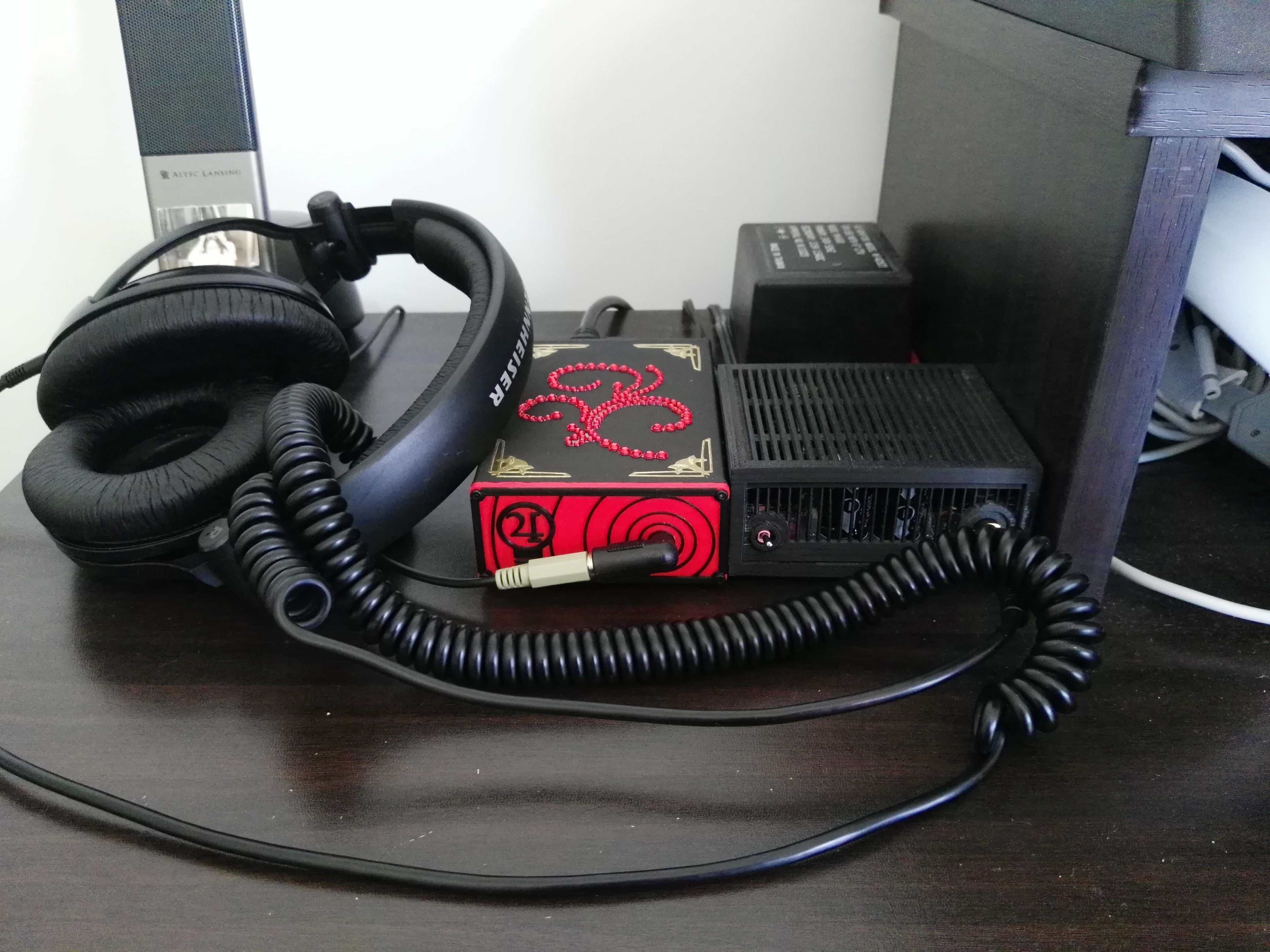
Finally, a use for my variac!
![]()
The grid-2-audio case (Autodesk Inventor design) fits in quite nicely next to my headphone amp (TinkerCAD design). Oh how I've improved my case making skills.
![]()
Yes, I know there are no waveforms to show yet (sorry!) - This will change very soon!
-
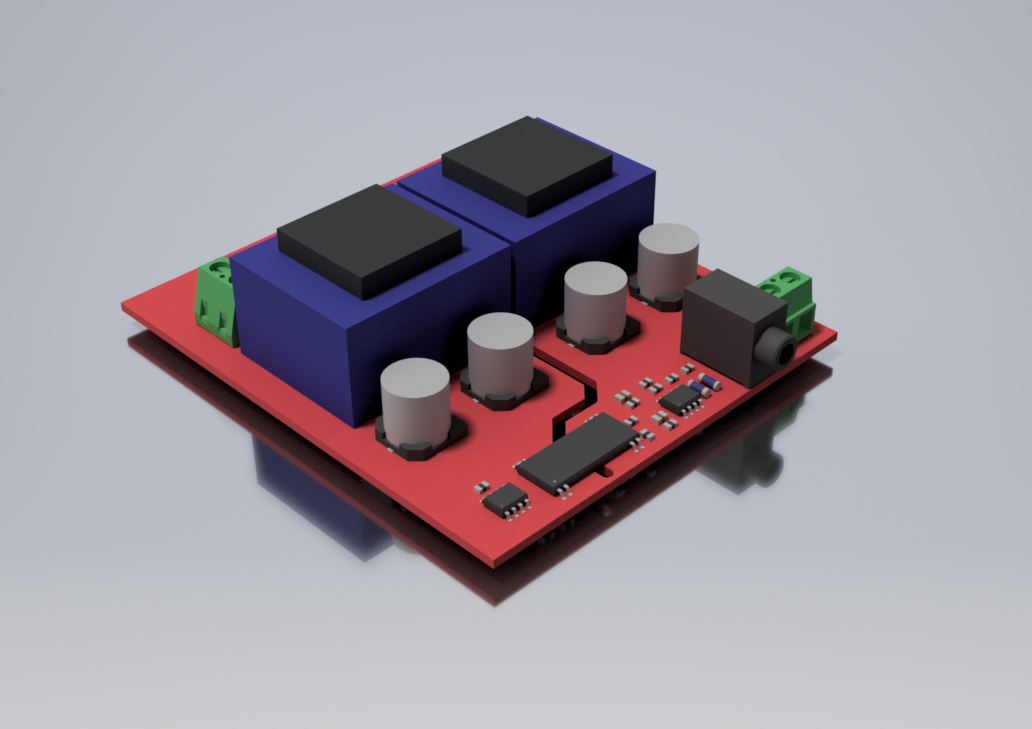
PCB Soldering Complete
09/30/2018 at 10:51 • 0 commentsThanks to my loving Father who has soldered every single component to the PCB for me, I am now in possession of a fully populated grid-2-audio PCB!
Have a look:
![]()
![]()
There was an issue with finding the correct capacitor for C22 due to a BOM numbering issue, but this has since been corrected (phantom C25).
Testing should be able to begin Tuesday night - Very exciting stuff! :)
-
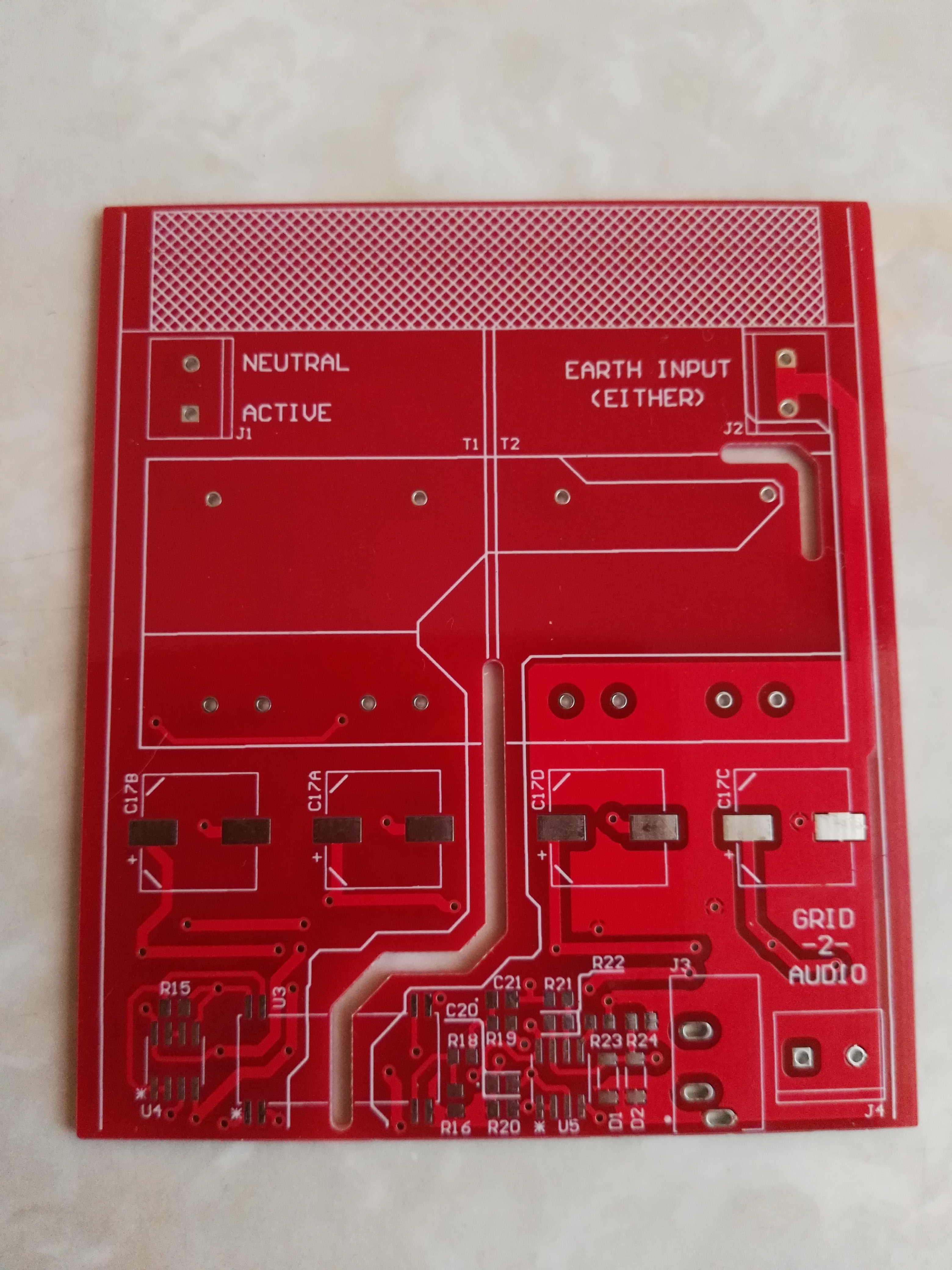
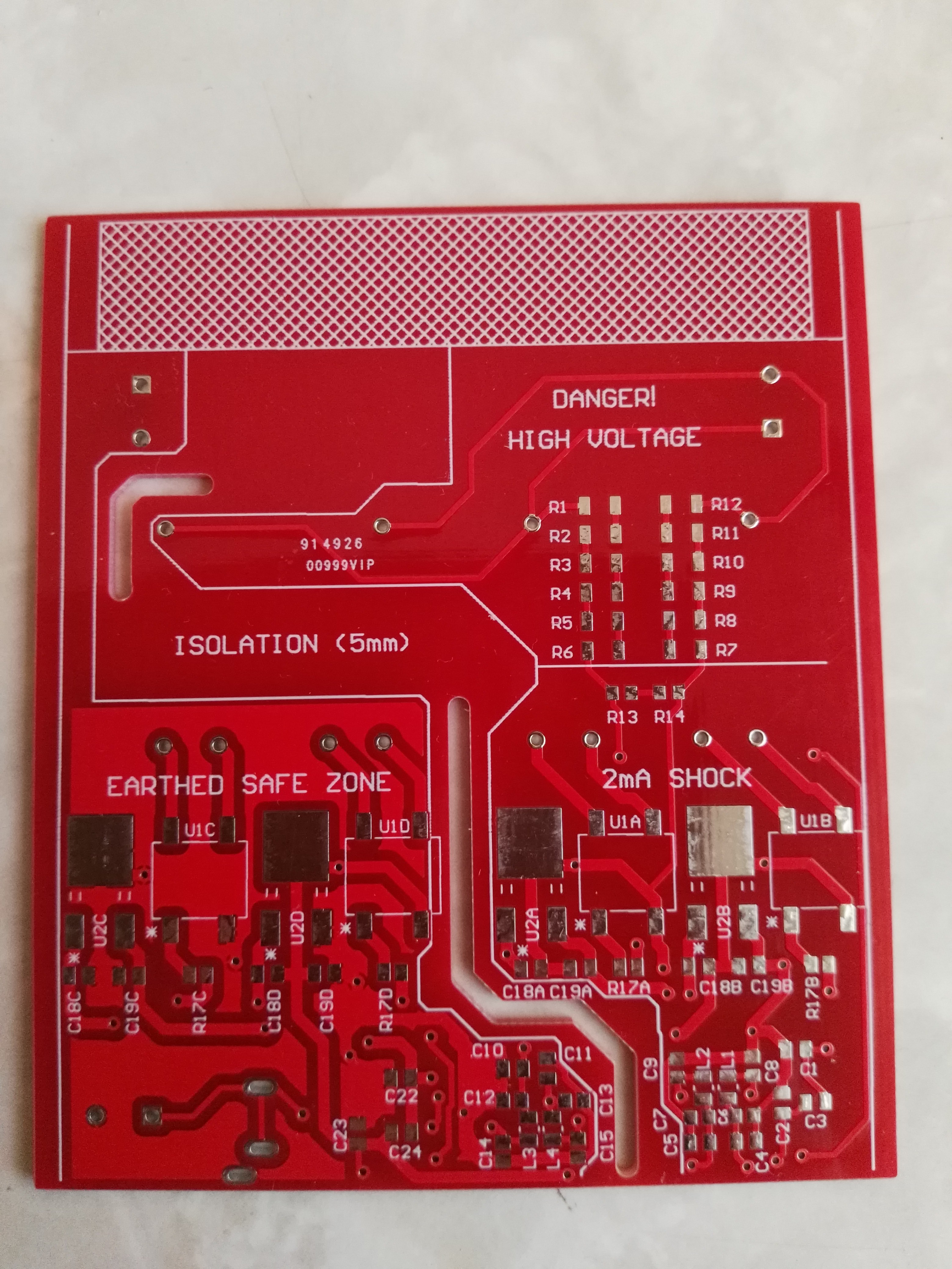
PCB Version 2 Bare Boards
09/29/2018 at 13:53 • 0 commentsSeems to be all in order!
Top view:
![]()
Bottom view:![]()
Manufactured by the Seeed Studio Fusion PCB service.
It's not long now until I'll actually have something to show for my efforts! -
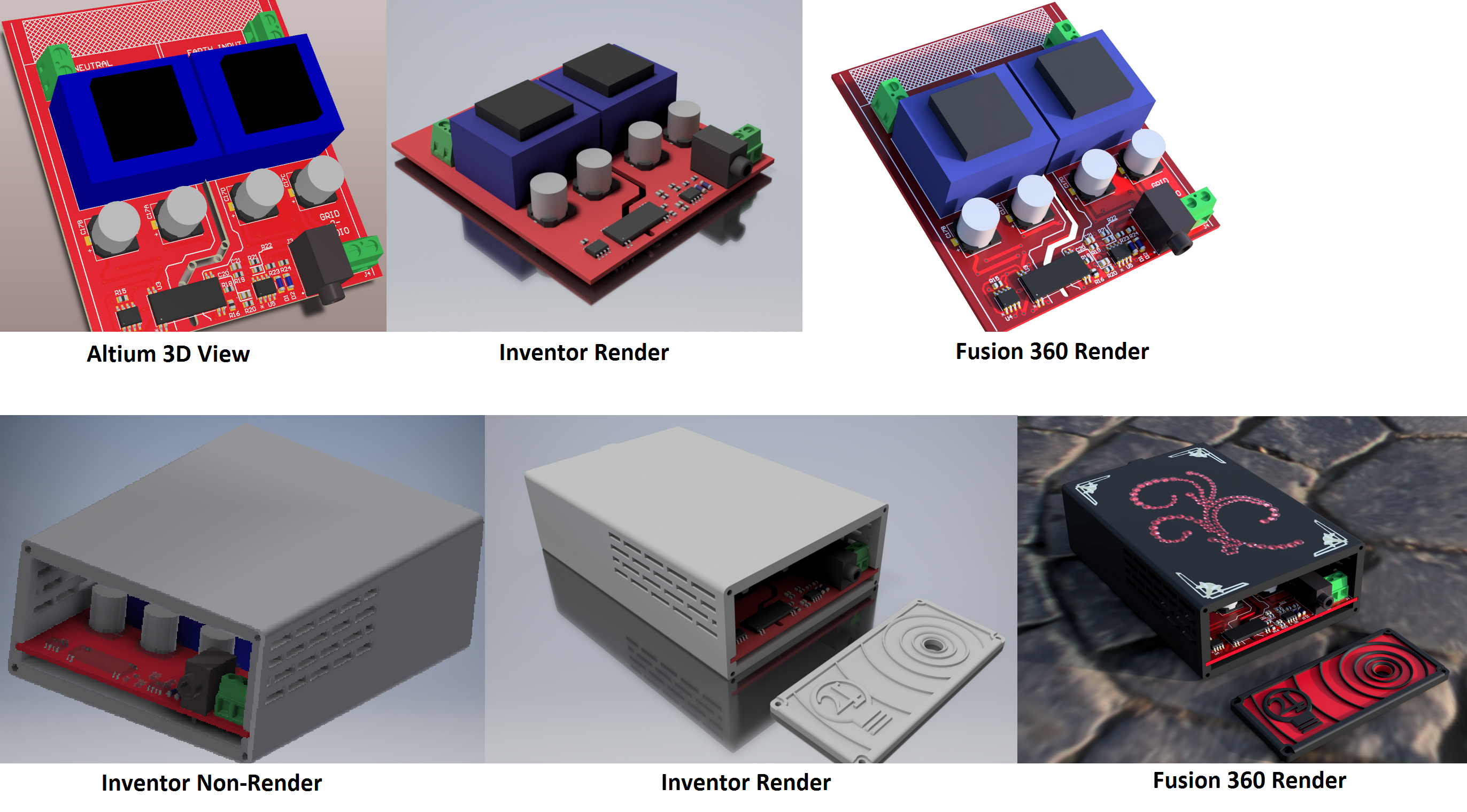
So in Summary...
09/28/2018 at 13:35 • 0 comments![]()
Use Fusion 360? Practice makes perfect? Something like that. At least I know where to start when it comes to 3D modelling after all this time. I've accomplished my Autodesk goal! :)
To anyone that wants to also produce these types of renders, here are the following steps:
1. Export your Altium PCB as a step file and production ready gerbers.
2. Upload your Altium gerbers to https://gerber-viewer.easyeda.com/ and use the top/bottom views to export 2D images.
3. Open the PCB step file in Fusion 360 and use the decal function to place your 2D images of the PCB as textures for the step file itself (as Altium doesn't export traces, etc. easily). Do this for both the top and bottom.
4. Enter render mode, set up the material type for any components that look odd (matt shades look best) and set the environment to the plaza for maximum lighting.
5. Start the render (not in-canvas render) on maximum settings and turn on the transparent environment option if you want a white background for the final exported render.
6. Wait 15-30mins and enjoy!
(In other news the PCB construction starts tomorrow!) -
Ray Tracing In Autodesk Inventor!
09/11/2018 at 11:07 • 0 commentsJust as a distraction, I found the ray tracing button in Autodesk Inventor and decided to abuse it:
![]()
![]()
![]()
![]()
![]()
And of course I just had to for comparisons sake:![]()
I had way too much fun making these ray tracing renders! They did take 20-40 minutes each with 100% CPU usage though...
(Not sponsored by Nvidia).
Make sure to check out the project log just before this one as I uploaded two at once. -
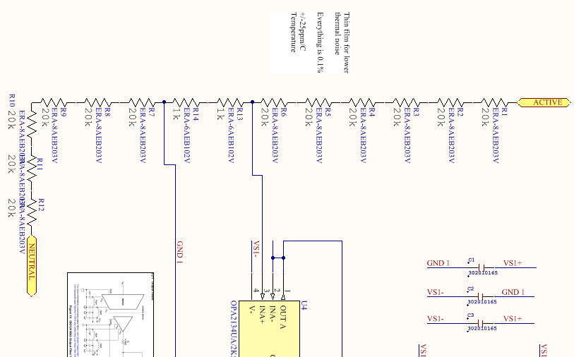
Version 1.0 --> to 2.0 Changes and File Uploads
09/11/2018 at 10:46 • 0 commentsSo first of all, all of the design files have been uploaded (well, the newest versions anyway) and are available for download. The original intention of this project was to make a nifty little product and sell them on eBay. However, due to some bad economic decisions with the component selections, I can't see the grid-2-audio unit being profitable in small batch production. As a result (and to Hackaday's liking) I'll just upload all of the design files here for anyone with a non-commercialisation intent.
Summary of 1.0-->2.0 PCB changes:
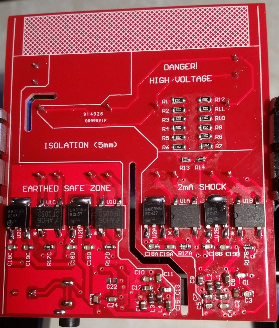
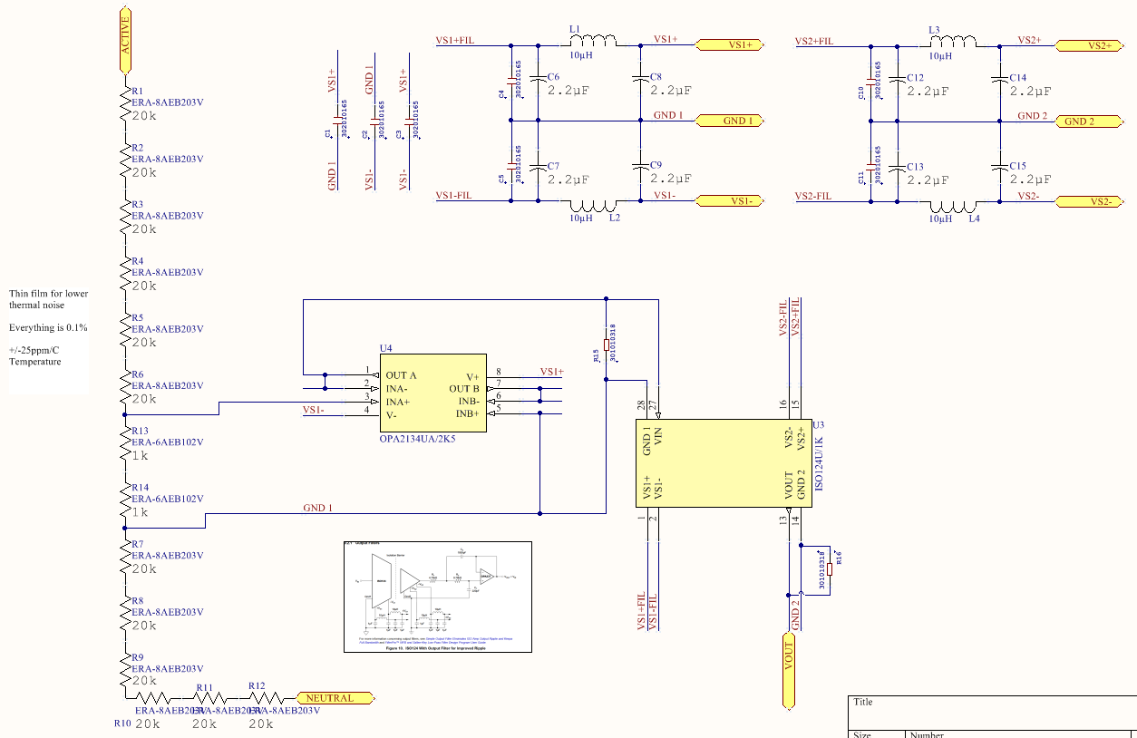
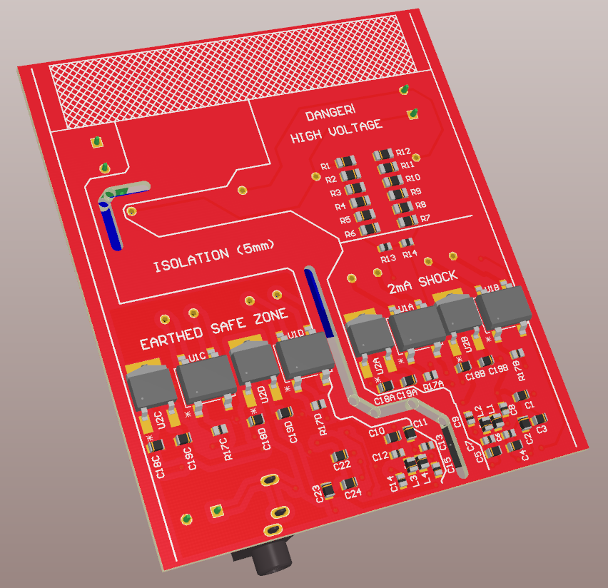
Number 1: Safety! The obvious safety concerns were the clearance from the mains potential to earth and the short-circuit shock capability of the mains measurement circuit should it be touched/connected.
-->There are two dangerous regions: The mains active/neutral region (lethal) and the signal processing region that is referenced to the mains (current limited during shocks). The voltage divider across the mains has been increased from 60kOhms to 240kOhms. Based on the arrangements the practical shock hazard of this region has now dropped from a ~7-8mA shock to a ~2mA shock. This is no longer dangerous even if a person were to experience it (it still hurts). Increasing the resistance of the mains voltage divider sounds like it would introduce noise, however this is not the case as the actual voltage difference is measured across 2kOhms. The divider acts like a 2kOhms in parallel with 240kOhms to the following op amp and so any noise is effectively dampened. However, that 2kOhm resistance is at the limit of what the opa2134 op amp can tolerate before another circuit is recommended by the datasheet (not to mention the op amp’s input capacitance starts to affect the upper frequency bands at 2kOhm).
![]()
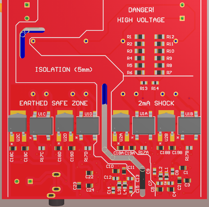
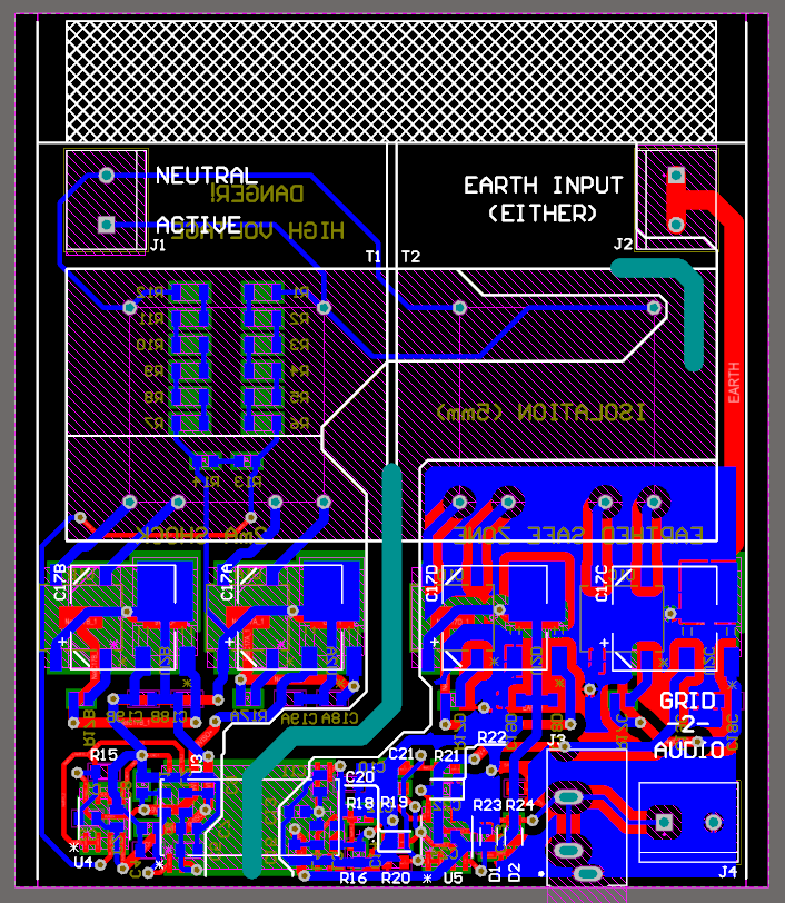
-->The minimum clearance between the earthed section of the circuit and the hazardous regions of the design was increased from 2mm to 5mm. This certainly is clearance enough from the "2mA shock" region, but I also added some 2mm cutouts in a region where the active connection comes within 7mm of the safety earth. Cutouts were also added throughout most of the isolation region just for the sake of good practice to maximise the creepage distance where ever possible:
![]()
Number 2: Footprints…
-->The 3.5mm headphone jack footprint that I downloaded did NOT have slotted cutouts! Although the 3D model did and the footprint pads were elliptical, I missed this completely. This has since been corrected.
-->Fixed all of the 100nF bypass cap issues with gerber viewers. Although the final V1.0 PCB turned out okay, the manufacturer’s gerber viewer wouldn’t display the 100nF pads at all (only the top solder cutout for the pad). I simply went into the footprint and deleted/recreated every piece of geometry and it fixed the problem?!?
Number 3: Stupid mistake.
-->This is a good one. I connected ground of the 3.5mm audio jack to the output signal and vice-versa. I’m glad I caught this because it’s the kind of mistake you can live with (using an adaptor cable) and be reminded about constantly for the rest of your life.
->
-->
--->
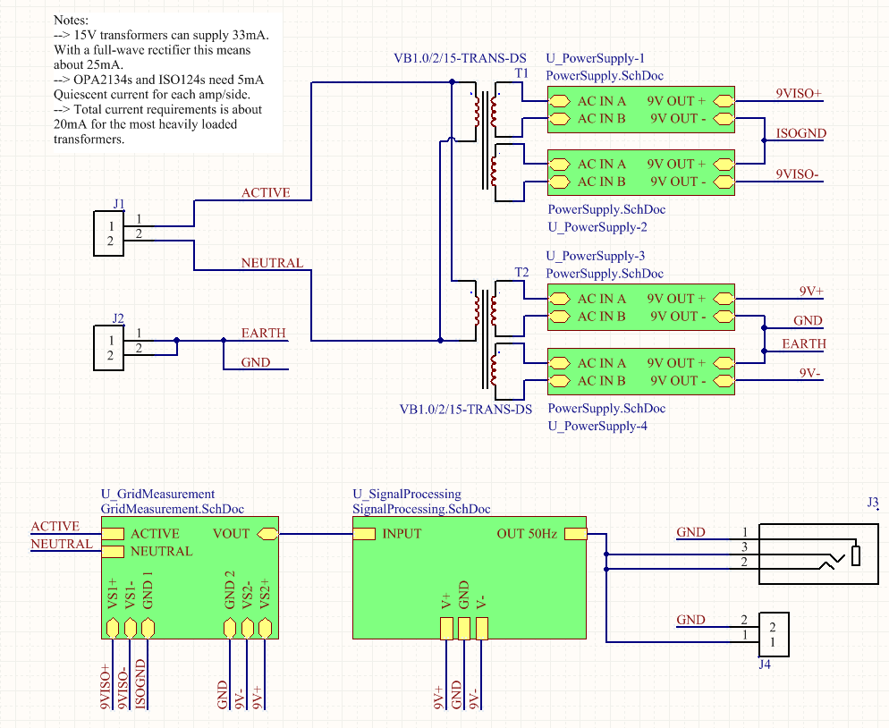
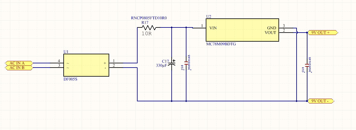
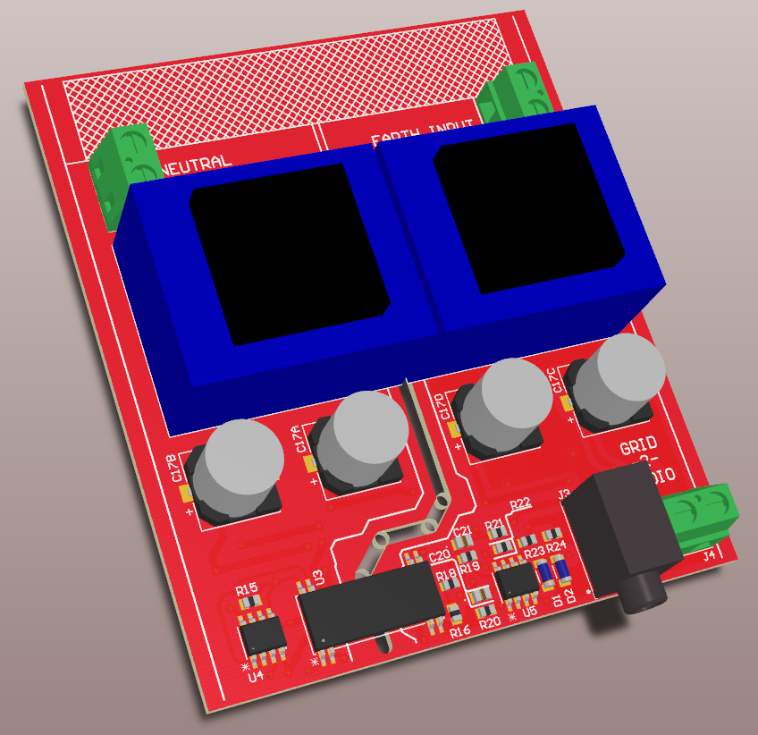
Right, now with that out of the way I present the “final” schematics/layout pictures, which are ALL available in the project files directory in Altium form:
![]()
![]()
![]()
![]()
![]()
![]()
![]()
-
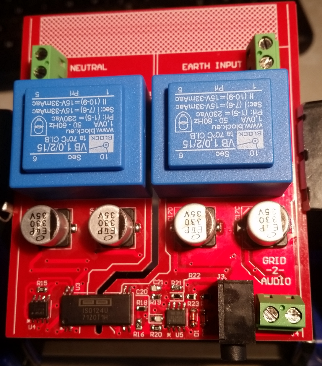
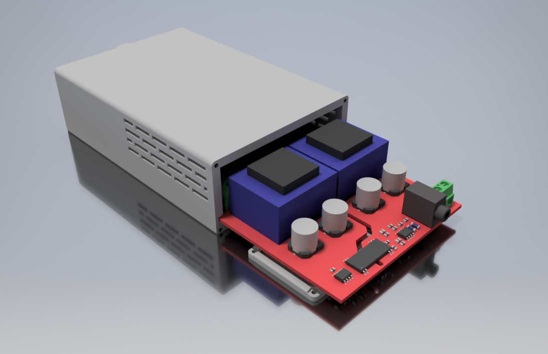
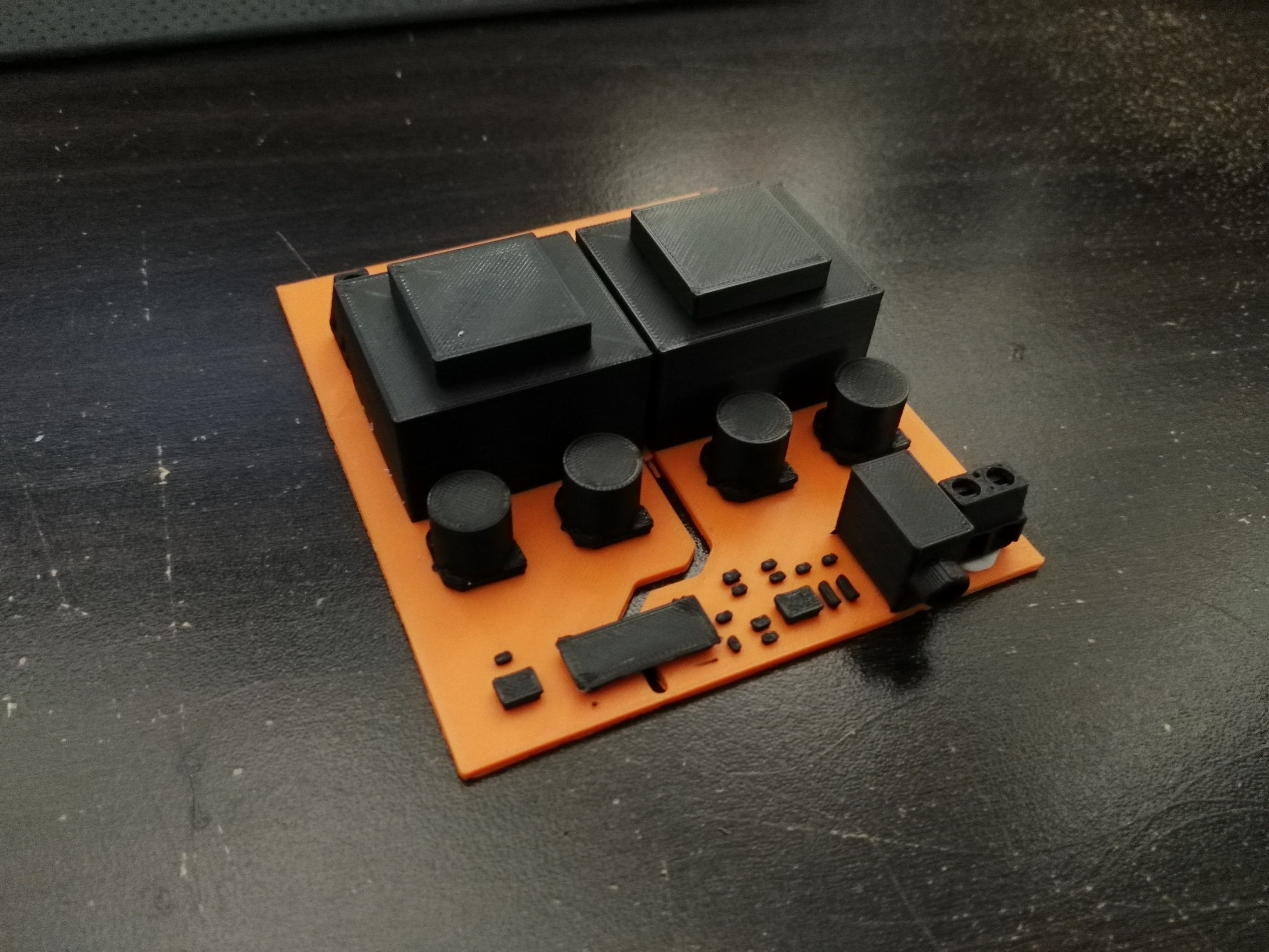
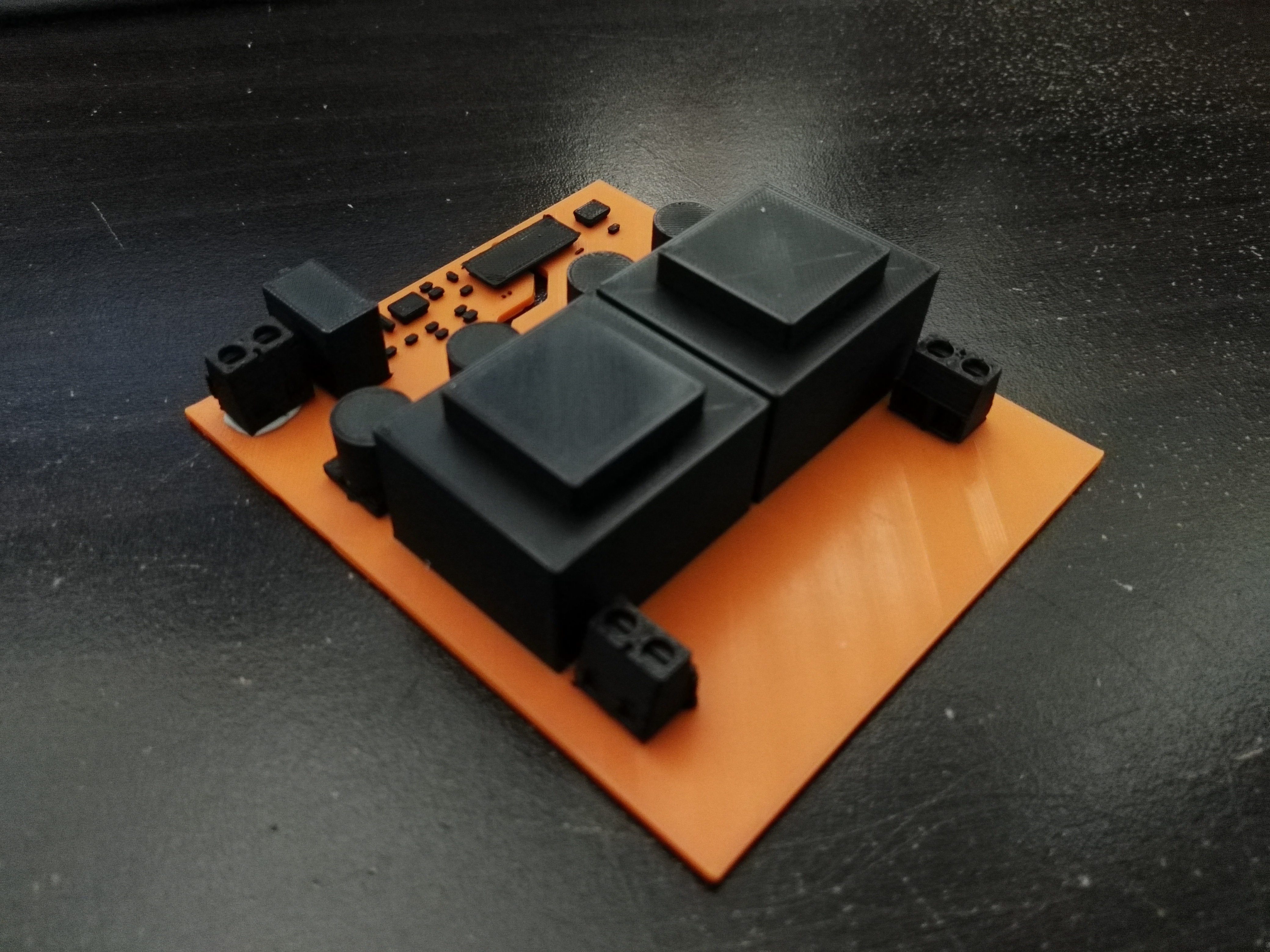
Very Accurate PCB Fabrication/Assembly
09/08/2018 at 02:55 • 0 commentsThe new boards arrived and assembly is complete:
![]()
![]()
![]()
![]()
Project complete.
Grid-2-Audio
A convenient adapter to view the electrical grid waveform through your PC's sound card.

 And a spectrograph:
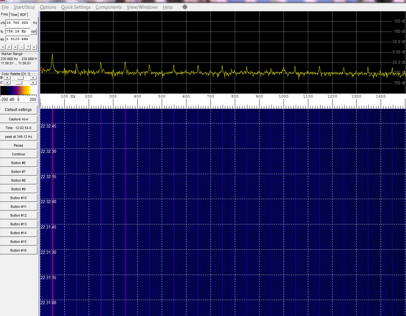
 This was taken over a two hour period (8:10pm - 10.00pm) on a Saturday night in Adelaide. Although the voltage magnitude is nonsensical, the proportional values are very relevant. The frequency plot, however, is correct is it's measurements.
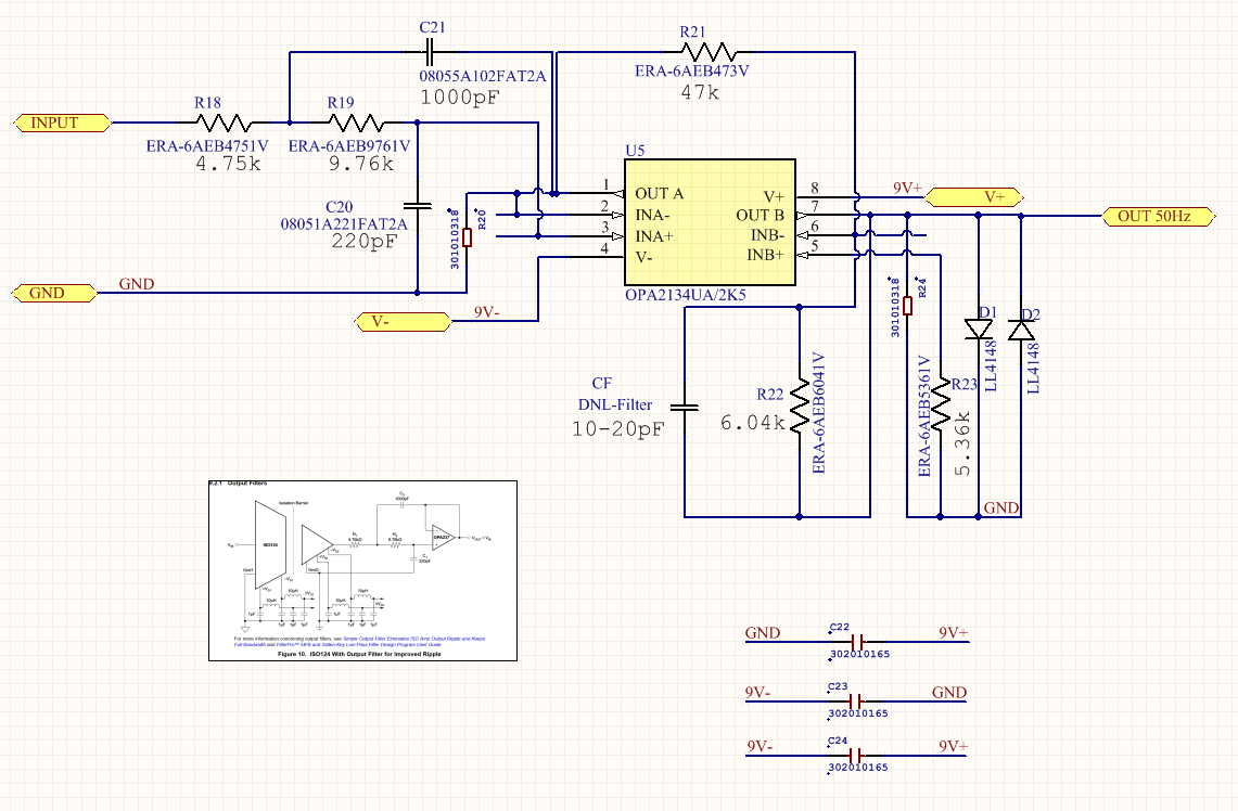
 Say I might, it's a flashlight!