 jaromir.sukuba
-
ADC input problems, again
12/11/2015 at 21:43 • 0 commentsIn one of my previous project logs I had problems with my MCP3424 ADC - it had too high input current - ie. low input impedance, making problems with high impedance voltage divider on input. Now, I've run into problems again.
After doing first crude tests and discovering that it works and really measures voltages and resistances, I got annoyed by huge error near zero voltages or resistances. Higher (more than a few hundreds Ohms) resistances were OK, but short circuit was indicated as something like 100Ohm, that's fishy for sure, so I started to investigate.
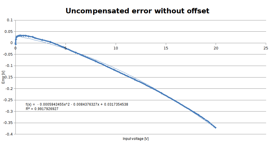
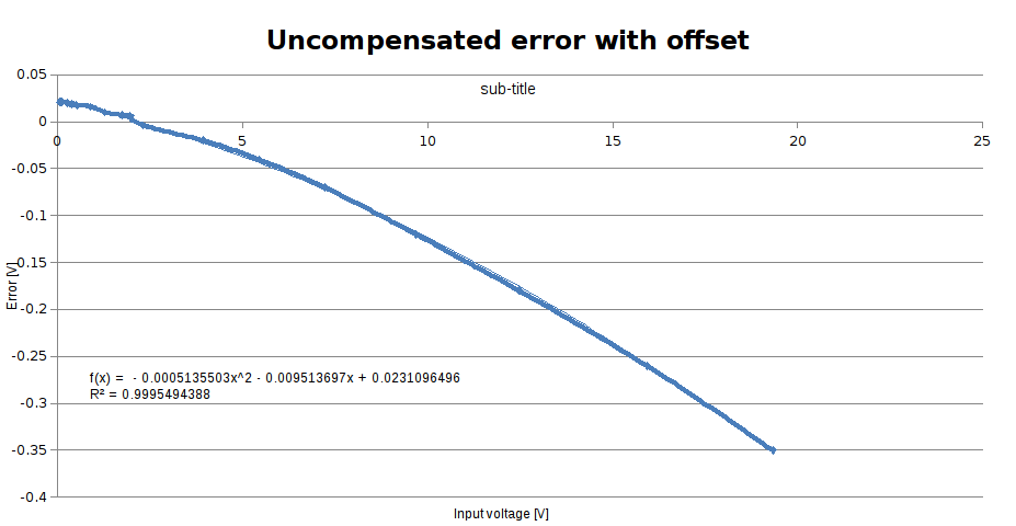
I did manual rough calibration of the device in two dozens of points between 0 and 20V, with somehow more points at the beginning of range:
![]()
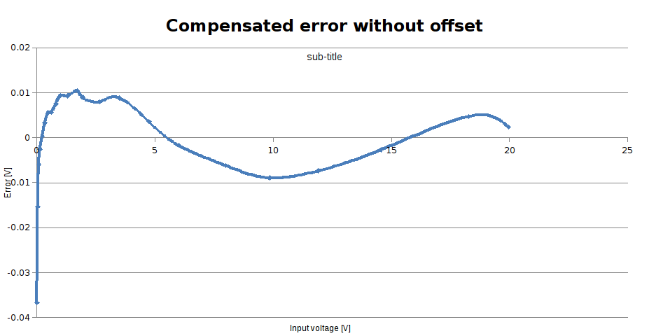
Well error increases almost linearly with input voltage - this looks like input divider isn't exactly accurate, but this could be treated by software calibration as long as the divider and reference voltage is stable, calibration and error correction is something I expected from the beginning. Problem is that the error isn't monotonous function - if you look carefully, it is rising at the very beginning of the curve (low input voltages), then falls slowly down as input voltage rises. Simple quadratic correction does its job, but compensated error is still not that good, especially at low voltages.
![]()
Almost 40mV at the beginning of voltage range is a bit too much.
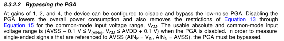
Well, offset rising at low input voltages? That sounds like problem with rail-to-rail input which is never actually rail-to-rail, but requires to be few milivolts above low rail and few milivolts under upper supply rail, but I double-checked the datasheet of ADS1120 and TI states that
![]()
TLDR - once the PGA is disabled (which is my case), the input voltage can safely go to ground level and shouldn't cause any problems. But it somehow does.
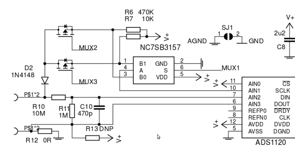
Fortunately, when drawing the schematics I had gut feeling that offsetting the negative input probe above ground level could be actually good idea. I reserved two components in the schematics - R12 and R13, one is marked as 0R and another one as DNP - do not populate. In this configuration, negative input is tied to ground.
![]()
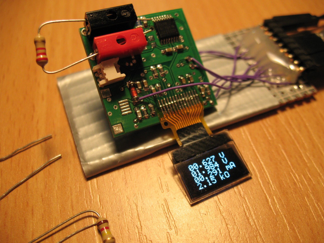
So I removed short circuit on place of R12 and inserted 200 Ohm resistor instead. On R13 position was placed 1k Ohm resistor, creating offset approximately 0,55V on negative input terminal. This offset doesn't directly interfere with measurement accuracy, as the ADC differential input still "percieves" only difference between input terminals. I performed the rough calibration again.
![]()
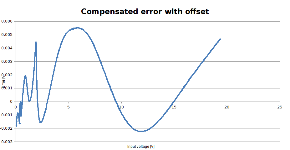
It looks similar to first calibration, but the nasty part at low voltages is completely gone, notice also the reliability factor of quadratic approximation went up from 99,2% to 99,95% and compensated error looks much better
![]()
The curve looks more shaky than before, but numbers on Y axis got one more zero in it. Maximum error decreased by almost one order of magnitude and shows no apparent systematic error. The error is now in order of milivolts (on 20V full scale range), and I'm pretty sure my DMM is not up to this task, so I have to obtain something better for more precise calibration. But anyway, even now is the accuracy much better than I expected - thanks to the two resistors.
Oh yes, and influence on resistors measurement accuracy was immediate - the 150Ohm resistor, indicated as something around 240Ohm before, is now absolutely correctly measured as 150Ohm. Nice.
For now, I'm calling this problem solved.
-
Working on firmware
12/09/2015 at 21:14 • 0 commentsI made some more work on firmware, wrote routines to support both voltage and resistance measurements and noted some facts:
1, Reference resistors R6 and R7 in schematics https://github.com/jaromir-sukuba/micro_progmeter/blob/master/hw/6c.sch.pdf should be decreased, something like one order of magnitude. When MUX3 signal is active and R7 engaged, measurement range is up to roughly 500kOhm, but the device is lacking precision under 500Ohm. On second range (MUX2/R6), the measurement range is well above 10Mohm - this is higher than expected. Something like 47k for R6 and 1k for R7 should move the measurement ranges lower into more useful range.
2, Even with no calibration/correction, the gain error and offset is quite acceptable, though I'm going to emply some kind of calibration.
3, The floating point routines are FLASH hungry, especially on SDCC with "not that finely optimized" libraries.
Above that all, it starts to look like a test gear, kind of.
Here are displayed debug values with measured resistance in last line. Close enough, for uncalibrated device.![]()
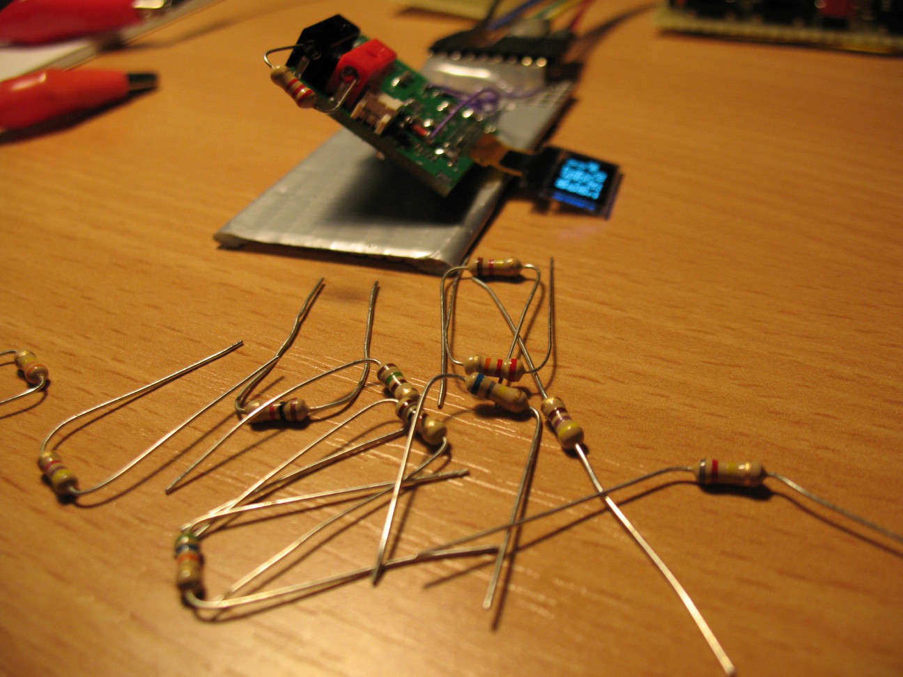
Bunch of resistors tested with this one. Those cheap carbon resistors are just for basic sanity testing, old precise resistor decade is still waiting for its job.![]()
-
HW rev. 2
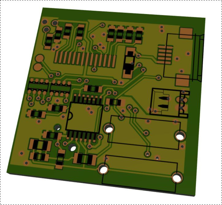
12/08/2015 at 15:13 • 2 commentsIt took me longer than I expected, but I finally had a few evenings of spare time to populate new board with components and do a bit of programming. Here is quick update of status:
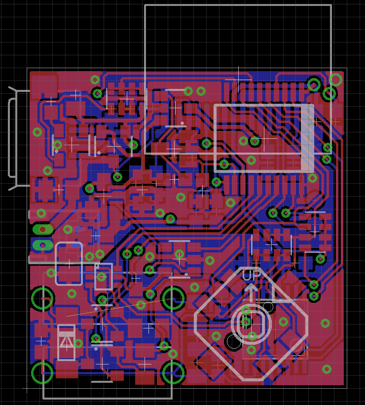
New PCB
Design in Eagle
![]()
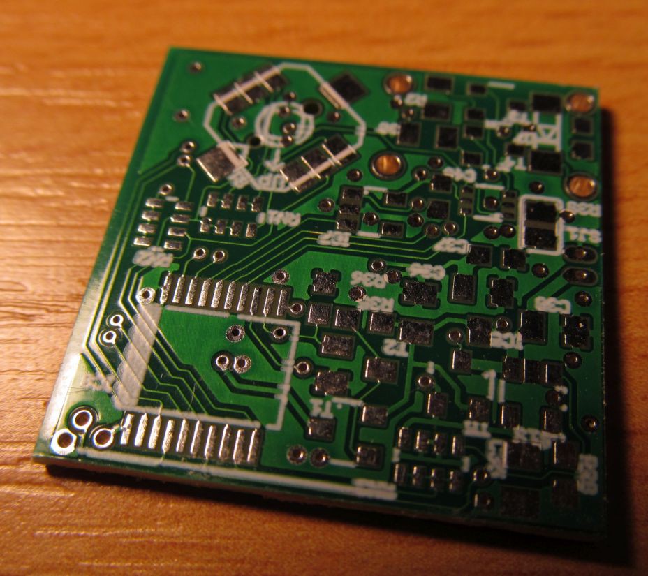
and in reality, manufactured by cheap local manufacturer it looks like this
![]()
The silkscreen isn't perfect for such as tiny board, but I don't care that much. The most significant difference to previous board is change of main ADC from MCP3424 to ADS1120. I had to free up four pins for full SPI interface, but the previous design was quite constrained in this aspect - so I opted to connect the joystick into resistor network and sense the joystick position by ADC. I left the original schematics on github as well as there is new one to compare.
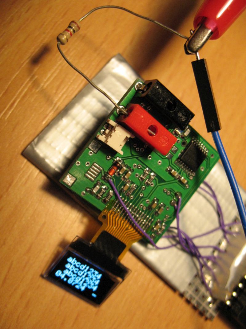
The new ADC works as expected and in fact, everything went flawless on first try. I reused "testbed" from previous hardware revision to continue with development
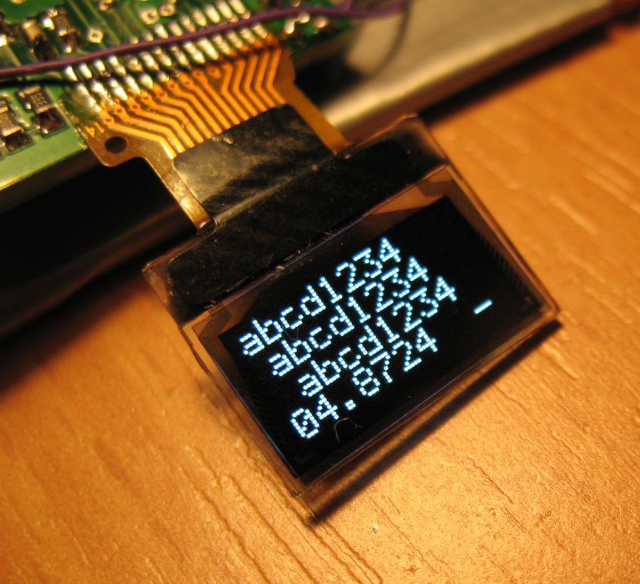
Testing code, showing measured voltage on last row.![]()
Yep, 4,87V on input. With PGA - internal to ADC - disabled, the smallest distinguishable voltage step is around 1mV even at 20V range and the readout is rock stable with no filtering, so it looks fine for now. With PGA gain set to higher than 1 and some digital filtering (PGA will bring some noise) I should be able bring down resolution well under 1mV - but anyway, even 1mV resolution is good for this meter.![]()
Firmware
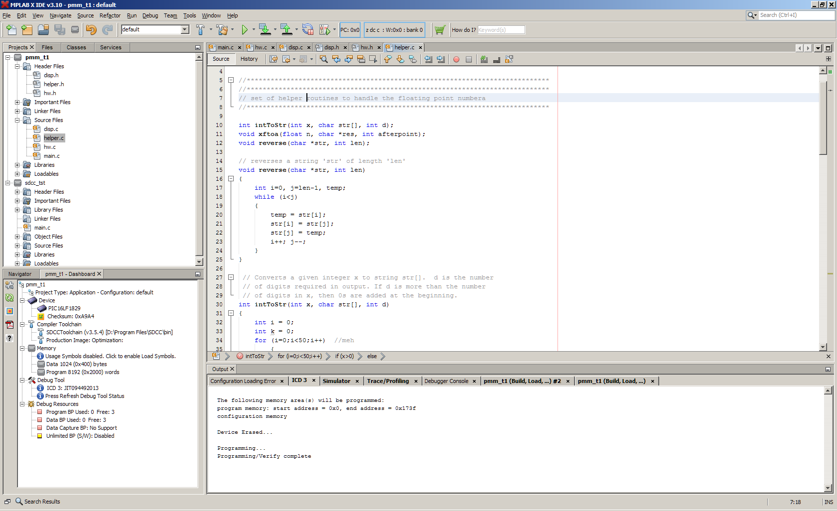
I'm writing the firmware mostly on my main Linux machine, but I don't forget on Windows users too. I'm using MPLABX suite from Microchip along with their XC8 compiler as well as SDCC. Compilation from command line without MPLABX should be easy.
For programming, I'm using Microchip ICD3 for now (cheaper PicKIt3 works well too), but as soon as I finish hardware for my #PIC16F1xxx Arduino based programmer I'll try it out too. This should allow maximum flexibility for project followers - you can build/flash it with MPLABX/XC8/PicKit3 for maximal convenience or command line/SDCC/my programmer for open-source tools.![]()
For now, I prepared basic skeleton of firmware, with ADC and display routines working with both XC8 and SDCC compilers, so I can start with more interesting parts. The firmware is available at github.
-
Input impedance woes
10/26/2015 at 16:51 • 0 commentsAfter sucess with digital part of the circuit, I tried to play with the analog too, not that successful, though.
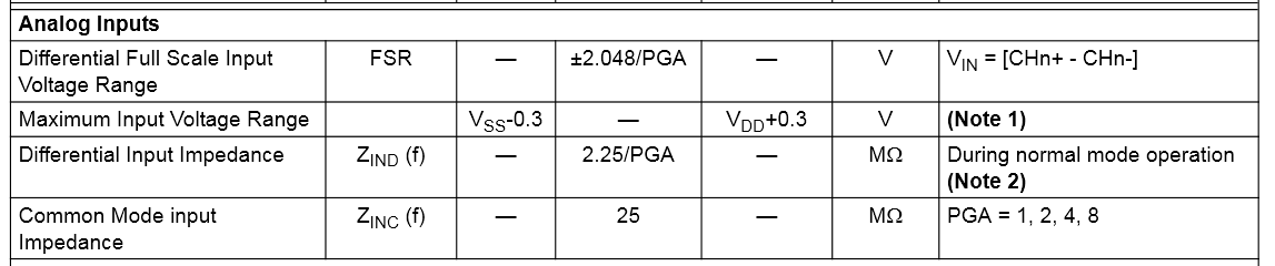
At the voltage measurment mode - MUX2 and MUX3 signals high see schematics - I applied voltage 4V at input terminals and measured voltage across R4. Considering the R4 value is diminished by 10Mohm (DMM internal resistance) in paralell (=910kOhm), one would assume voltage around 0,33V here. But I measured something slightly under 0,25V, resulting in my genuine confusion. Wait, there is nothing but resistor, capacitor and... ADC. Yep, ADC. But hey, it cant be the ADC contributing with such as huge error, because it has input impedance around 25MOhm, I checked it before. 25MOhm across 1MOhm would bring the measured voltage few percents down, but this is something I could tweak by software calibration (which would be needed anyway) - though now I'm looking at voltage few tens of percents down, which is suspicious. No, It can't be ADC, because I checked it, look:
25MOhm, here you go. 25MOhm of... common mode input impedance. But differential (between + and - input terminals) is.. drumroll... 2,25MOhm, one order of magnitude lower.![]()
1Mohm, 2,25Mohm and 10Mohm in paralell gives something around 650kOhm, with the 10Mohm upper divider we get to something like 245mV. Close enough to 250mV. I checked voltage across R6 - 1,7V or thereabouts, which is kind of expected. Then I switched active channel from 1 to 3 and voltage on R4 increased to cca 340mV and voltage on R6 jumped to 1V. Confirmed, ADC is doing all the bad things. I used the MCP3424 few times before and was quite confident about it, so I just skimmed through documentation and used it when doing design.
![]()
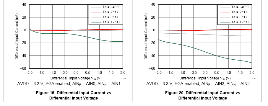
Now, after I found the problem and facepalmed long enough, some solution is expected. I went to mouser and tried to find some other 2-channel ADC with 16- or more bit resolution with acceptable package, here is what I got - not exactly long list. Seems like input impedance around 2Mohm with strong resistive component is common for other ADCs in this class too (like my favourite ADS1100 and similar ones), but ADS1120 looks like something I want.
Input current seems to be in nanoamps range, few orders of magnitude below MCP3424 solution.![]()
This ADC has downsides too - I have to sacrifice easy integration via I2C bus and it has only two input channels (compared to MCP3423), so I have to measure the battery voltage via other means. I has SPI interface, requiring 4 wires, along with additional ADC channel for battery measurement it means another five IO pins. Because the battery voltage divider has quite high resistance, connecting to ADC IO pin is problematic, single opamp in voltage follower circuit is needed. My favorite type for this job is MCP6041 - just like in my altimeter or microreader.
So, as I have only one IO pin unused, I have to find 4 more IO pins. There is more ways to solve this problem.
1, Joystick interface takes 5 IO pins, that's luxury for such as slow interface.
- I can save 4 IO pins by using PCA9536 via I2C (which is there for display anyway)
- I can save a few pins by connecting some of joystick pins into resistor network in this manner
2, There is one IO pin taken by charger state monitoring and another one is needed for battery voltage measurement. If I'd use two channel I2C ADC, I can save not just two IO pins, but also opamp. I'm going trade SOT-23 for another SOT-23, but saving IO pins.
3, Use two IO pins I dedicated to in-circuit debugging for something else. Ideally, the ICD pins should be kept free for debugging purposes, but with some care it could be shared for things like user switches or indication LEDs.
4, Using higher pin-count MCU. Most straight-forward solution, but takes precious PCB space.
5, Combination of some methods above.
Not sure about what to use, by now.
-
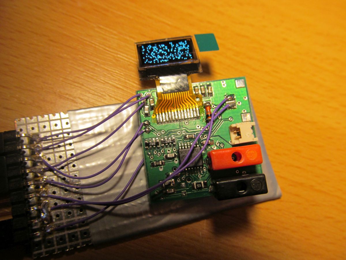
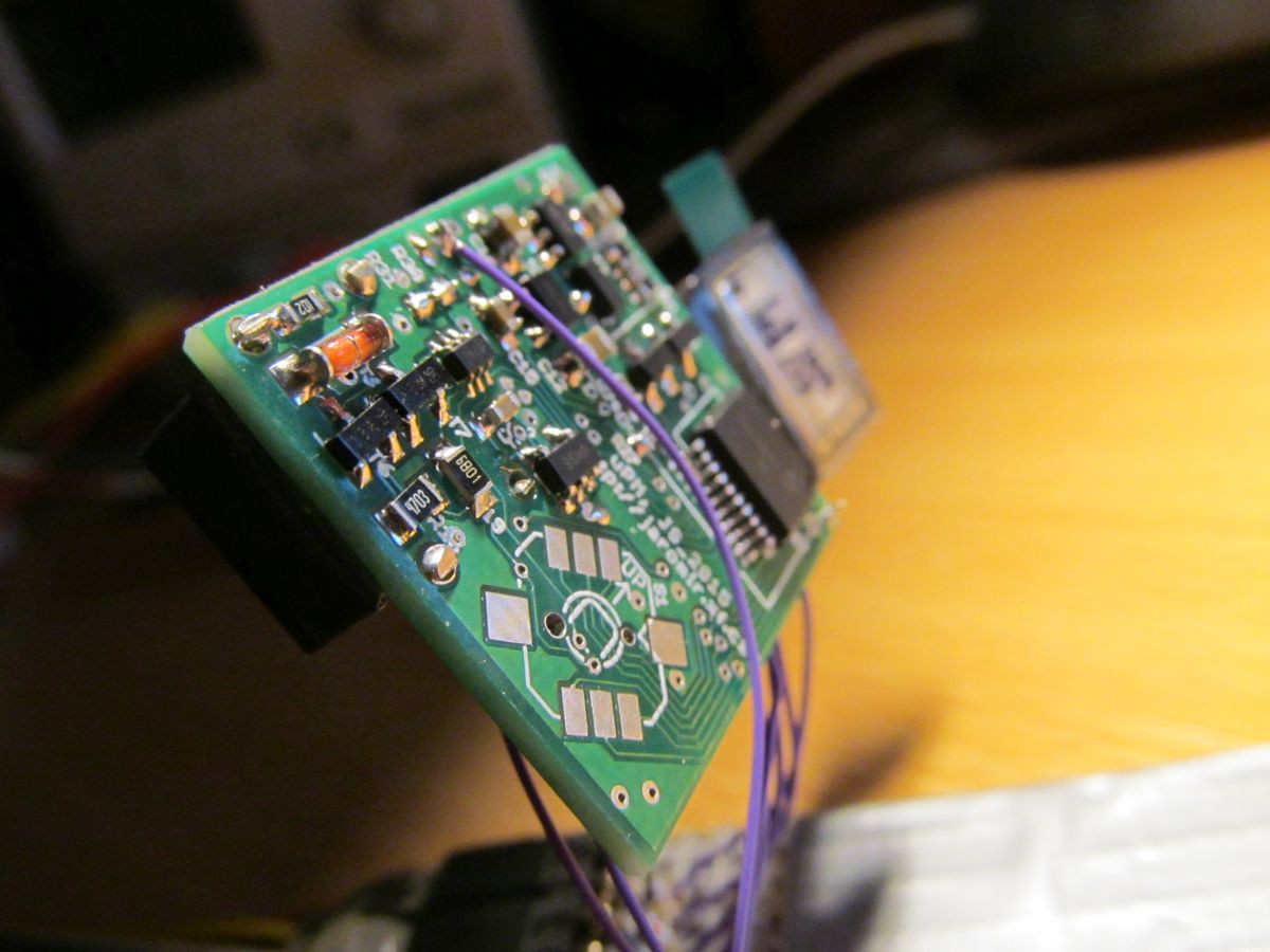
PCB assembled and works, sort of
10/23/2015 at 08:19 • 0 commentsLook at my PCB, look
![]()
For easier manipulation/programming work I soldered pinheader and a few wires to piece of universal PCB. The progmeter PCB with components is so tiny and lightweight that a few 30AWG wires lift it off the base board. For now, I made some basic functionality check - power supply circuits seem to work, MCU is alive and I can program it, display is OK and communicates via I2C, initialization of display works and it displays "noise" form power-on state of display RAM.
![]() But there isn't everything going just flawless. I found out that the flex ribbon on display is too short to bend over the PCB to get the display panel to other side of PCB, so it is on wrong side for now. The holes for 2mm banana terminals were too small - I had to drill it to larger diameter, losing hole plating material, so soldering the terminals was difficult and I had to glue it in place. I also found out that I2C bus pull-up resistors are connected to analog supply instead of digital 3V3 net, so the I2C debugging was quite confusing. Fortunately, it seems that all the problems can be fixed relatively easy. Yet I have to check the ADC and analog parts, then I'll proceed to PCB ver 1.1
But there isn't everything going just flawless. I found out that the flex ribbon on display is too short to bend over the PCB to get the display panel to other side of PCB, so it is on wrong side for now. The holes for 2mm banana terminals were too small - I had to drill it to larger diameter, losing hole plating material, so soldering the terminals was difficult and I had to glue it in place. I also found out that I2C bus pull-up resistors are connected to analog supply instead of digital 3V3 net, so the I2C debugging was quite confusing. Fortunately, it seems that all the problems can be fixed relatively easy. Yet I have to check the ADC and analog parts, then I'll proceed to PCB ver 1.1 -
Components, vol. 2
10/13/2015 at 21:51 • 2 commentsAnd here we are.
![]()
I had to buy a surprisingly lot of items, as I have mostly 0805 sized parts in my lab supplies. Nevermind, it's all in here, so I have to wait for PCBs - those should arrive in the middle of next week.
-
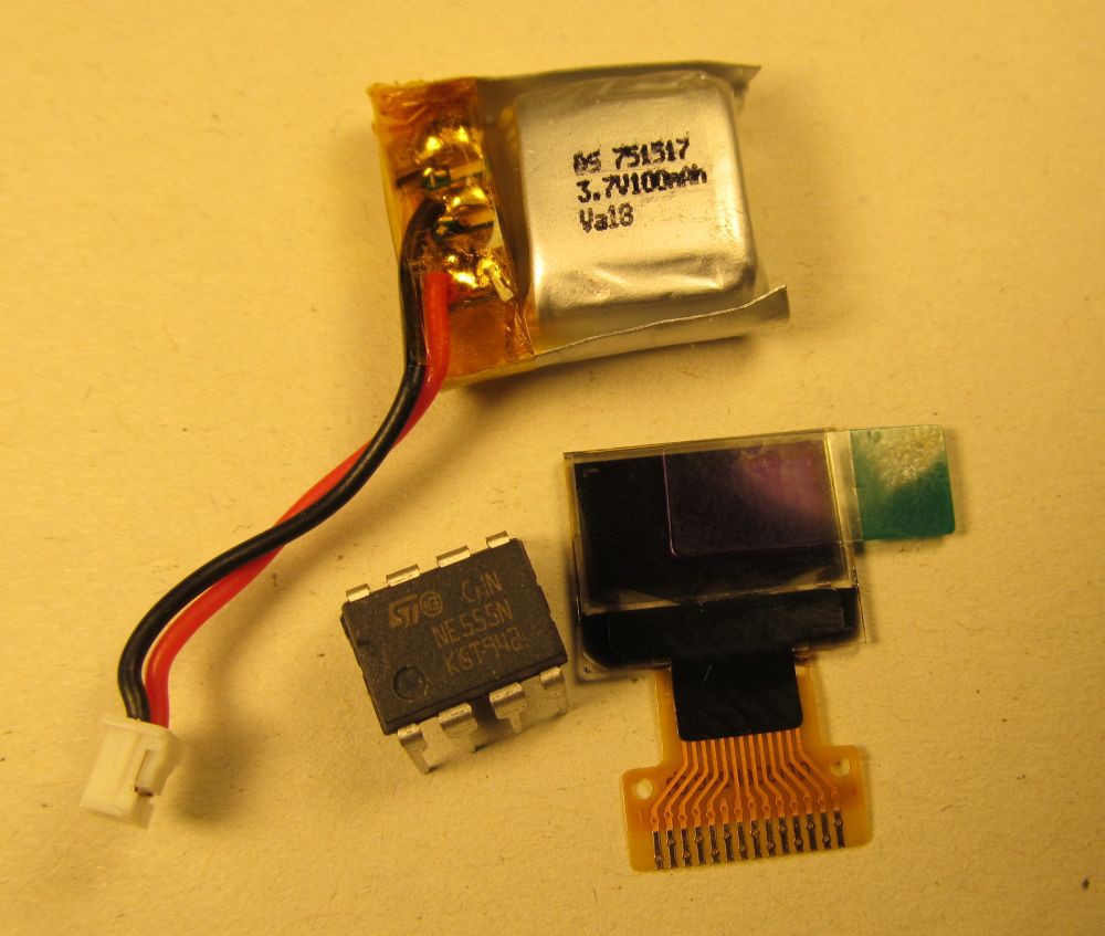
Components and "JST connector"
10/12/2015 at 11:57 • 0 commentsBecause I like projects logs with pictures, here we go:
Photo of display and battery with third object for scale. I thought of using banana for this, but settled down with 555 timer in DIP-8.
![]()
Those components are really tiny.
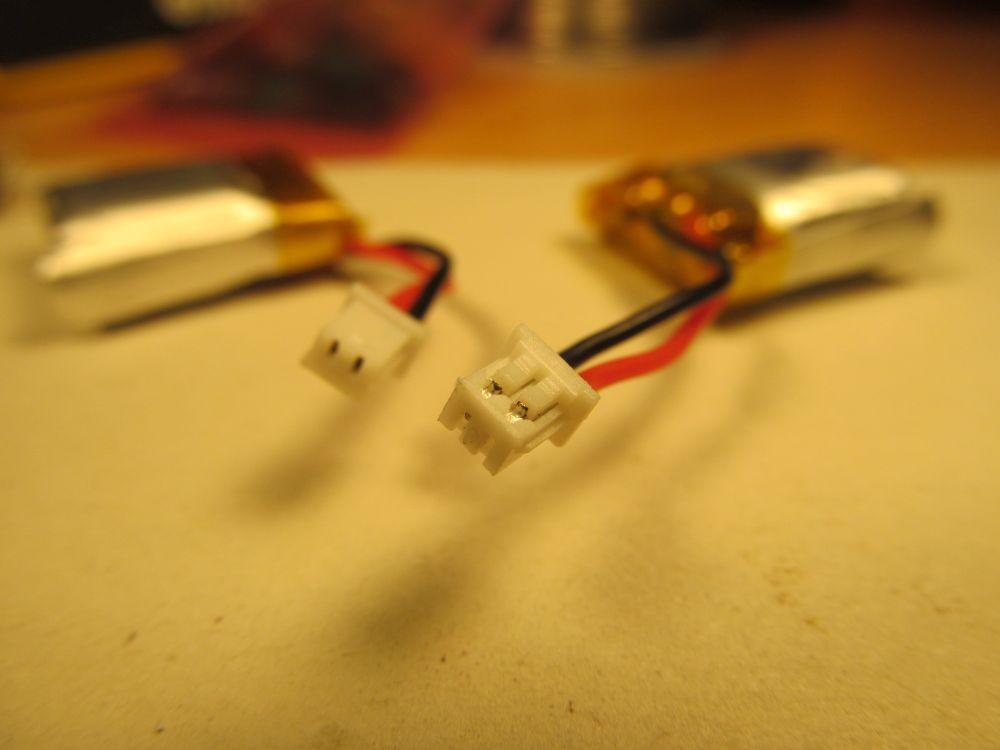
By the way, notice the connector on battery.
![]()
Sellers usually don't care and call it JST connector, though it isn't real JST. In fact, it has 1,25mm pitch and belongs to Molex Picoblade series. The exact part number for my application is Molex 0530480210. I bought it here though it is available at mouser or digi-key.
By the way, PCBs are ordered and I should receive it during next week.
-
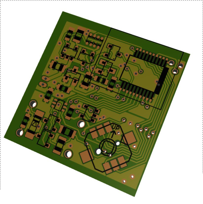
PCB design, rev. 1
10/09/2015 at 07:51 • 0 commentsWell, it wasn't really trivial to cram all the parts on the board, but I did it.
![]()
The grid is in 1mm (=0.0393 inch) pitch and board is 25mm (=1.55342798E-5 miles) wide and 25mm (=0.000273 football fields) long and was routed/components placed in 0,1mm (=0.258 ponits) grid.
I tried this online PCB viewer and the results look enjoyable.
![]()
When routing such as tiny board, the 0,16mm tracks looked really thick, 0,4mm vias somehow huge, 0603 components (most of the passives on board) a bit oversized and 0805 components (few precision resistors) like real giants.![]()
The PCB in Eagle format and schematics in easily readable PDF format is in github repository as expected.
-
Github repo
10/08/2015 at 14:39 • 0 comments -
First sketches
10/08/2015 at 13:14 • 0 commentsI set a few basic goals for this progmeter:
1, PCB has to be under 25,4x25,4mm in size to fit the rules of #The Square Inch Project
2, To be able to measure at least basic ranges of voltages and current. Say 20V and 10Ohm to 1Mohm with reasonable accuracy, say 1%. Some amount of foolproofness is required.
3, Completely battery powered
4, At least rudimentary math operations above the measured results.
Now, let's analyze it: The first point is nothing special in this phase of planning, just set PCB outline to 25x25mm. Third point is somehow complicating the first task, as the battery or charging circuit has to be placed on PCB. Last point precedes using of MCU, display and few buttons as user IO (opposed to using "dumb" ADC driving display). In fact MCU simplifies some hardware aspects of progmeter, as will be seen later.
Second point is where the fun begins.
Analog part
Measurement of voltage is fairly simple, just take an ADC. Internal ADC of most of MCU's would be sufficient, to some degree. If I'd use 10-bit ADC, for 20V range I'd get around 20mV resolution (20V/1024 levels) which is not bad, but not that great on voltages below 2V. Usage of external ADC allows better results. 12-bit ADC is marginally good, but higher resolution ADC's are not that expensive those days. MCP3421 costs 2EUR in single quantity locally and is switchable from 18-bits to 12-bits, allowing compromise between speed and resolution. So, we have ADC and voltage divider - in fact, voltmeter.
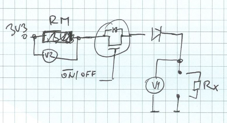
Resistance measurement is a little bit trickier. The most obvious method requires precise current source with known value and voltmeter to measure voltage drop on that resistor. Note that resistor instead of current source will not work, as current flowing through unknown resistor will vary with the DUT resistance. If I could measure the voltage drop on that known resistor, I can calculate current flowing through it and subsequently unknown resistance.
![]()
When MOSFET is on (its gate is grounded), current flows from 3V3 source through Rm, diode and Rx to ground. Voltage drop U1 on Rx is measured by voltmeter V1, Rm is known and voltage drop U2 on it is measured by V2. The resulting resistance is
where
so that
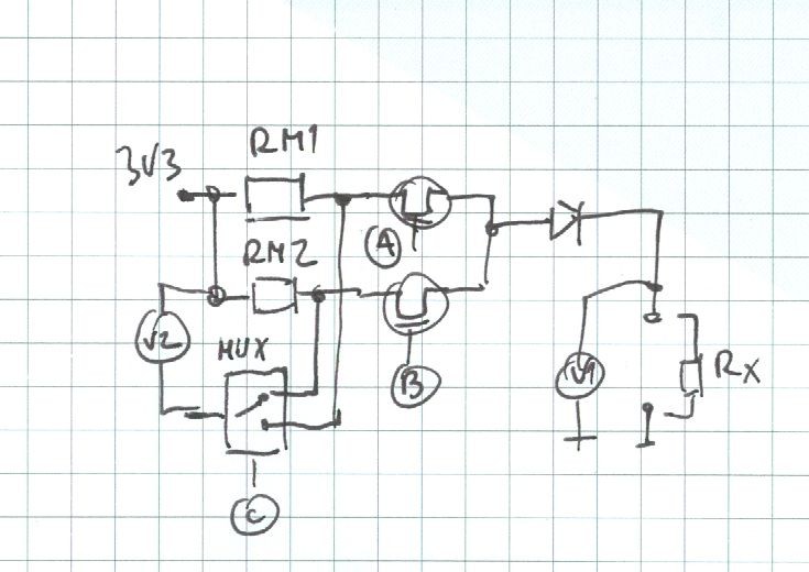
Diode serves as simple overvoltage protection and is not needed by principle of operation. Resistance range from 10Ohm to 1MOhm spans through five decades and single resistance range will not cut it, obviously. Adding another resistance range makes it simpler, requiring two and half decade per range and this is bearable for low-spec device. The resulting schematics for resistance measurement will look like this
There are two MOSFETs, each one able to switch Rm1 or Rm2 resistor. There is also switch, selecting the proper resistor for V2 input.![]()
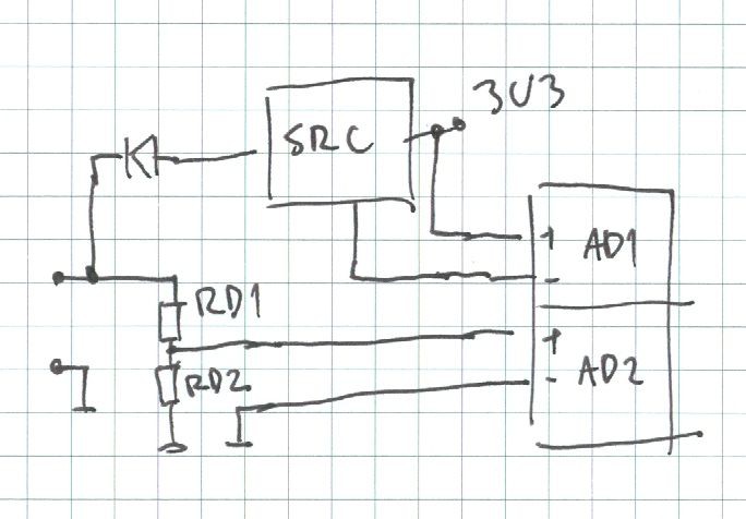
Now let's put it together:
The switchable "current source" SRC leading to on differential AD input, resistor divider formed by Rd1 and Rd2 is connected to AD2. Two separate ADCs are not needed, I can simply use double input ADC, like this one.![]()
Now I have completely analog-to-digital frontend. ADC communicates via I2C bus and MUX / MOSFET control lines are simple 3,3V digital lines.
Digital part and board space
I opted to use some low-end 8-bit PIC MCU for this task. In fact,I could use anything with a few IO lines, but this is the simplest way to make it working what is fine when making time constrained contest entry.
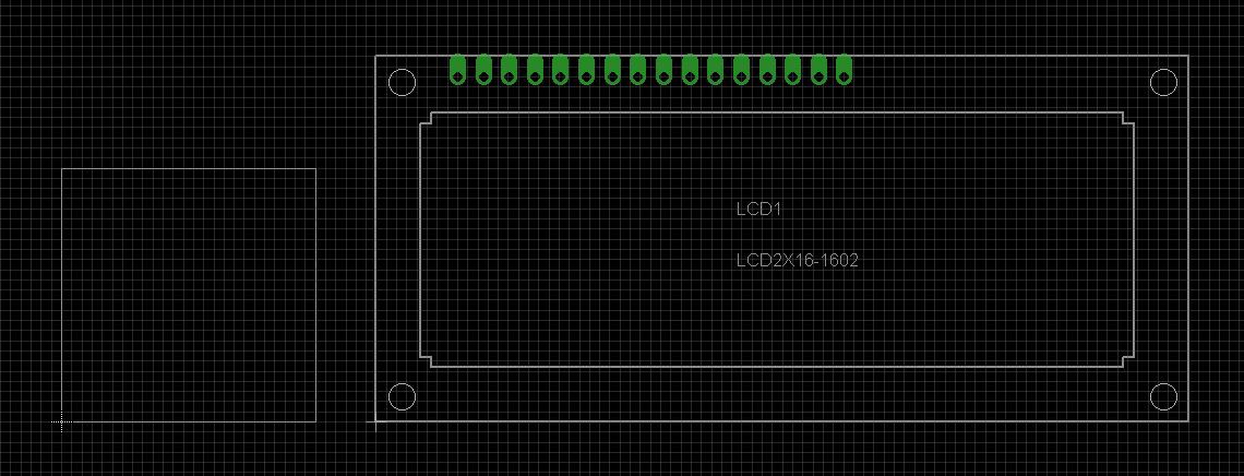
For user IO there is not much of choices, given the fact I have to cram it into 25x25mm area. This is now classical 16x2 LCD looks next to 25x25mm square.
![]()
Meh. I have to find something smaller.
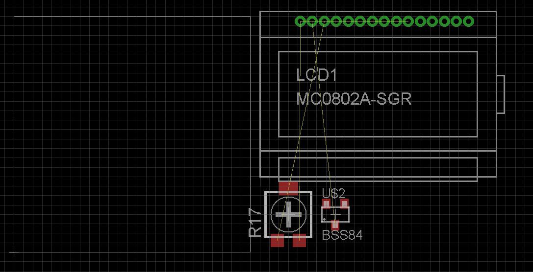
This is how the MC0802-SGR display - I used it in #Mini Altimeter - looks, with trimer and switching MOSFET.
![]()
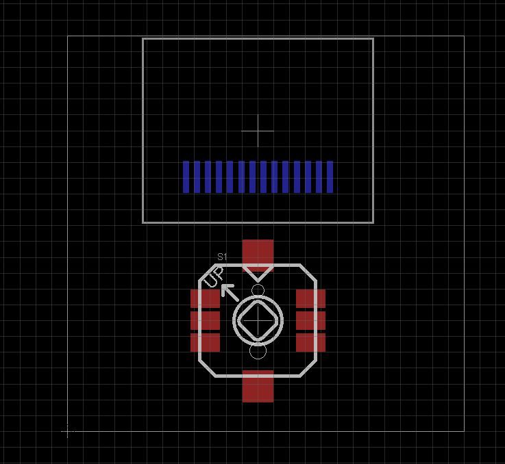
Better, but still way too big. Then I remembered I found 0,49" inch OLED on aliexpress and bought it, thanks to my slight compulsive hoarding disorder. Coupled with micro joystick it looks like a nice couple
![]() Let's add some MCP73831 for Li-Ion charging and micro USB connector and we have it!
Let's add some MCP73831 for Li-Ion charging and micro USB connector and we have it!

 But there isn't everything going just flawless. I found out that the flex ribbon on display is too short to bend over the PCB to get the display panel to other side of PCB, so it is on wrong side for now. The holes for 2mm banana terminals were too small - I had to drill it to larger diameter, losing hole plating material, so soldering the terminals was difficult and I had to glue it in place. I also found out that I2C bus pull-up resistors are connected to analog supply instead of digital 3V3 net, so the I2C debugging was quite confusing. Fortunately, it seems that all the problems can be fixed relatively easy. Yet I have to check the ADC and analog parts, then I'll proceed to PCB ver 1.1

 Let's add some MCP73831 for Li-Ion charging and micro USB connector and we have it!