slisgrinder
-
LOG 20180522: Serious Business...
05/22/2018 at 22:52 • 0 comments![]()
So, there is a reason for the lull in project activity and its serious business!
No, seriously, its business. I have decided to make this into a business venture but don't worry, its still the same project goal and its still open source. If you haven't noticed it yet, there is a change in the project banner with the company name (although I had the name on the PCBs for a while). I am in the process of getting everything formalized (lots of paper work and legal/regulatory obligations) which justifies the inactivity of the project.
In my previous log I mentioned something about manufacturing my own LEDs by combining dies into a single package. I explored more on that idea which spawned my decision to make it into a formal business venture. Of course I have to do the usual market research and what not but I see an opportunity here.
Please stay tuned as things progress, I don't want to get ahead of myself here...
In the mean time I'll just leave this here:
PS: Glove and Boots could really use your support if you haven't already seen their material on YouTube!
-
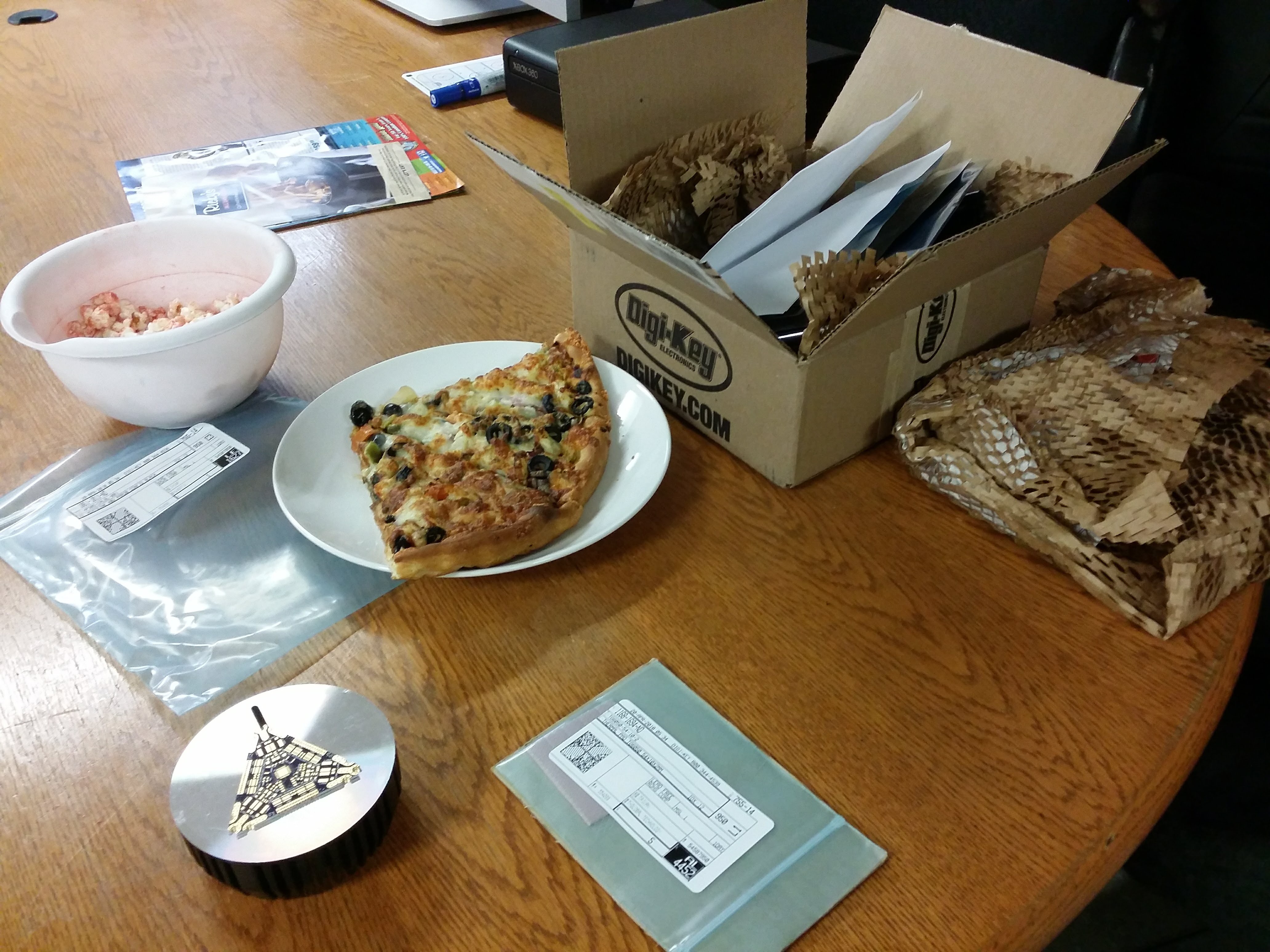
LOG 20180425: Test fixture
04/26/2018 at 02:17 • 0 commentsI ordered parts for another cell to be populated with the appropriate emitters for the GTGL variant.
![]()
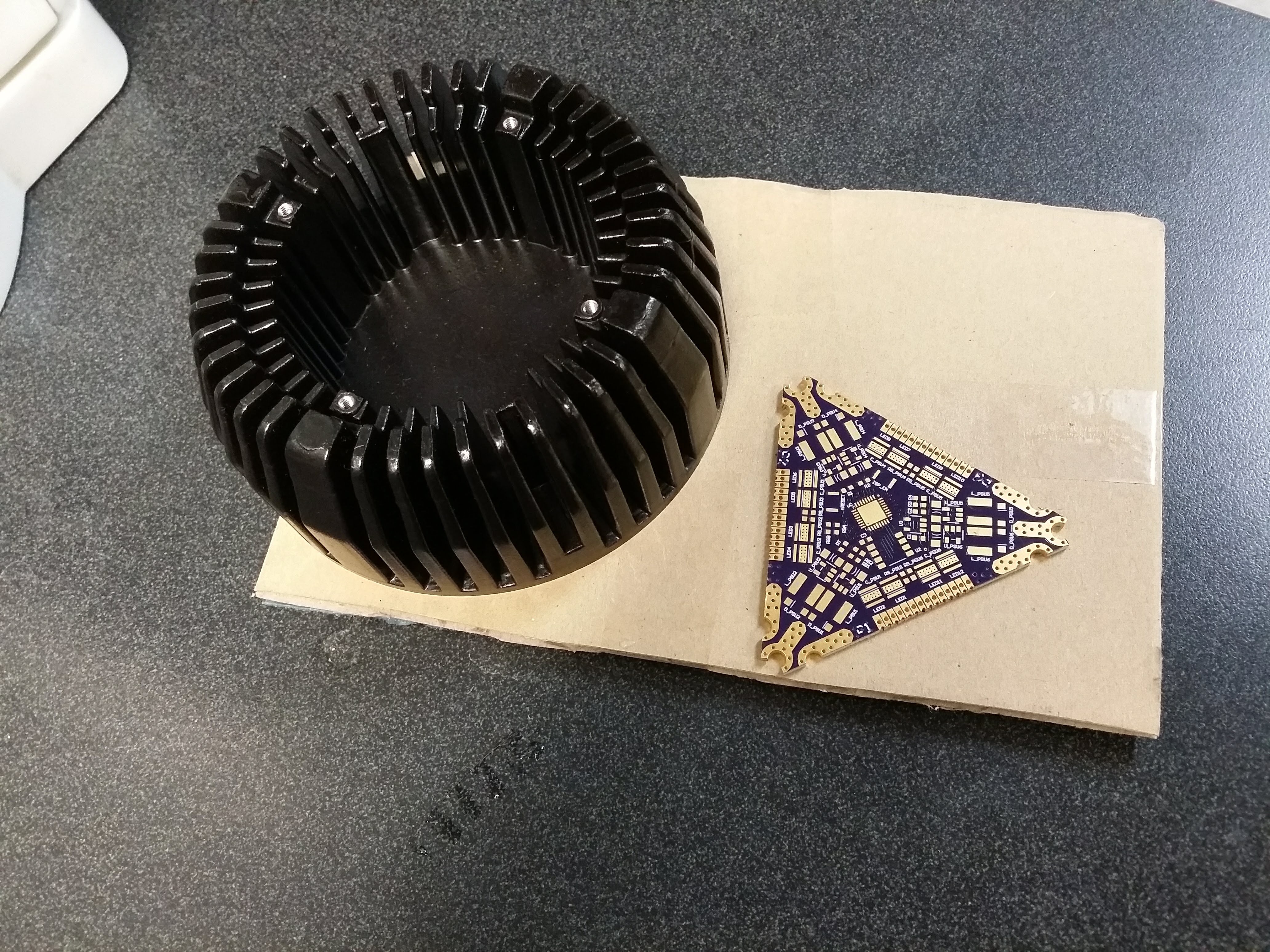
Along with the order I included a semi beefy heatsink and thermally conductive pads that I'll use as a test fixture.
![]()
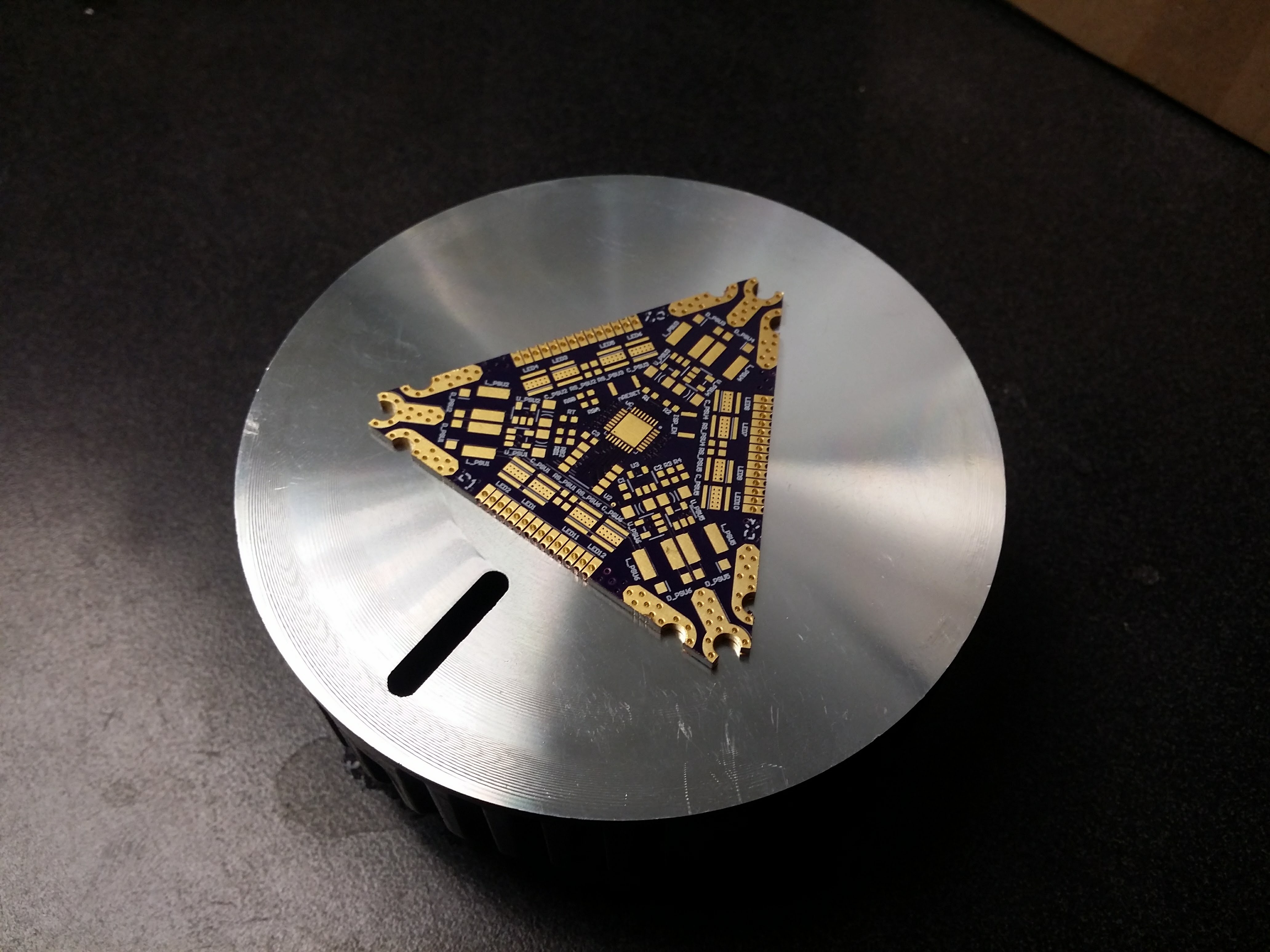
The plan is to drill and tap 3 holes that coincide with the 3 ground holes on the PCB. This way I can do code development without worrying about overheating the board. I can also look into the thermal performance of the PCB and its layout. Hopefully this will yield results that I can later use for designing proper thermal management.
![]()
I had very many insightful conversations on the #HackChat in regards to designing, manufacturing and implementing thermal management for MOSAIC LS. There are many factors to account for and it is most definitely not easy to design a heatsink let alone to manufacture one. None the less, the task of thermal management has been put on the back burner until MOSAIC is ready in both code and electronics.I would personally like to thank everyone on the HackChat that has helped me out. I am very grateful to everyone for pitching in ideas, debating designs, exploring options and just all round fun. This is a great community and I hope it continues to be so.
On a side note, I came upon an idea (which I initially had but dismissed due to inaccessible manufacturing) that to make electronic, optical and thermal management design easier, why not make my own LEDs? Actually, why not just assemble my own LEDs?
Cree and other manufacturers sell just the LED die to manufacturers who then do the potting/gold bonding/eutectic attachment process and sell them. There are a couple of manufacturers who do make COB grow lights but their price point is too high which MOSAIC LS is trying to address. However if MOSAIC LS were to evolve into an open source COB LEDs with the same design goals for a lower price point then there might be something further to explore.
There would be the same 4 variants (AHLS, GTGL, GAGL and GUVL) but as a COB. This would be smaller, have more consistent optical properties and have simpler thermal management. Also, open source COB LED!
-
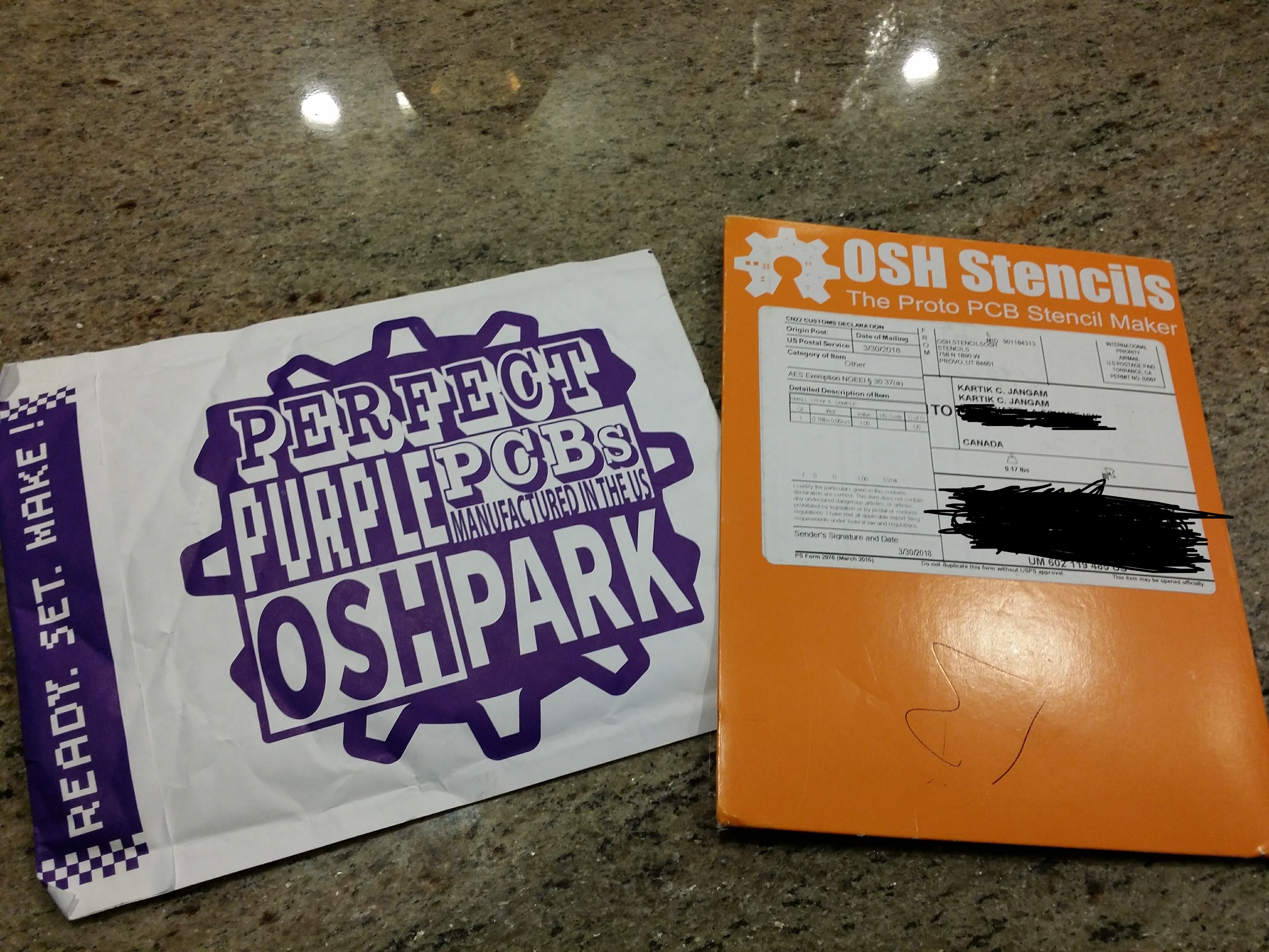
LOG 20180414: Revised PCB and Stencils!
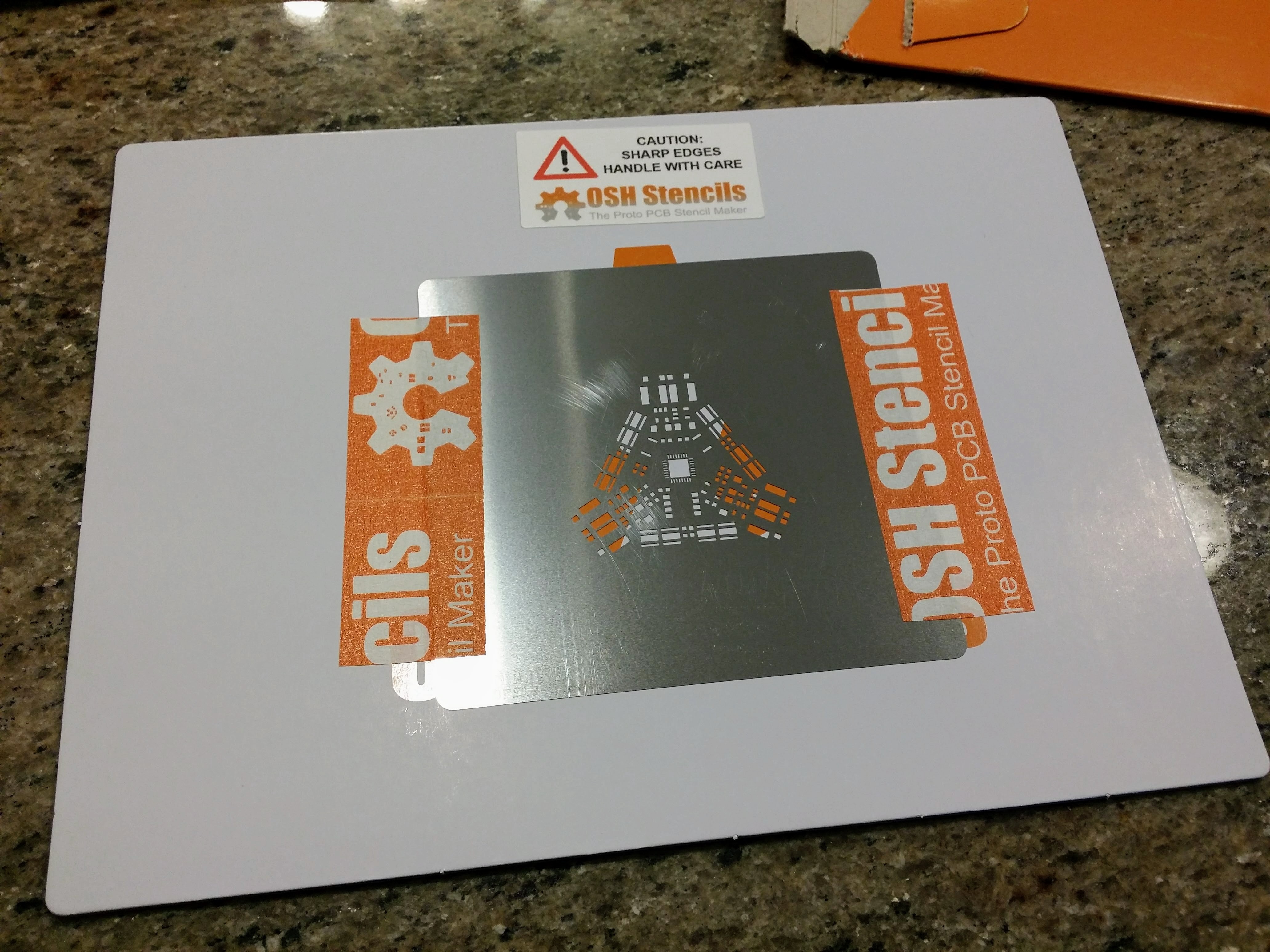
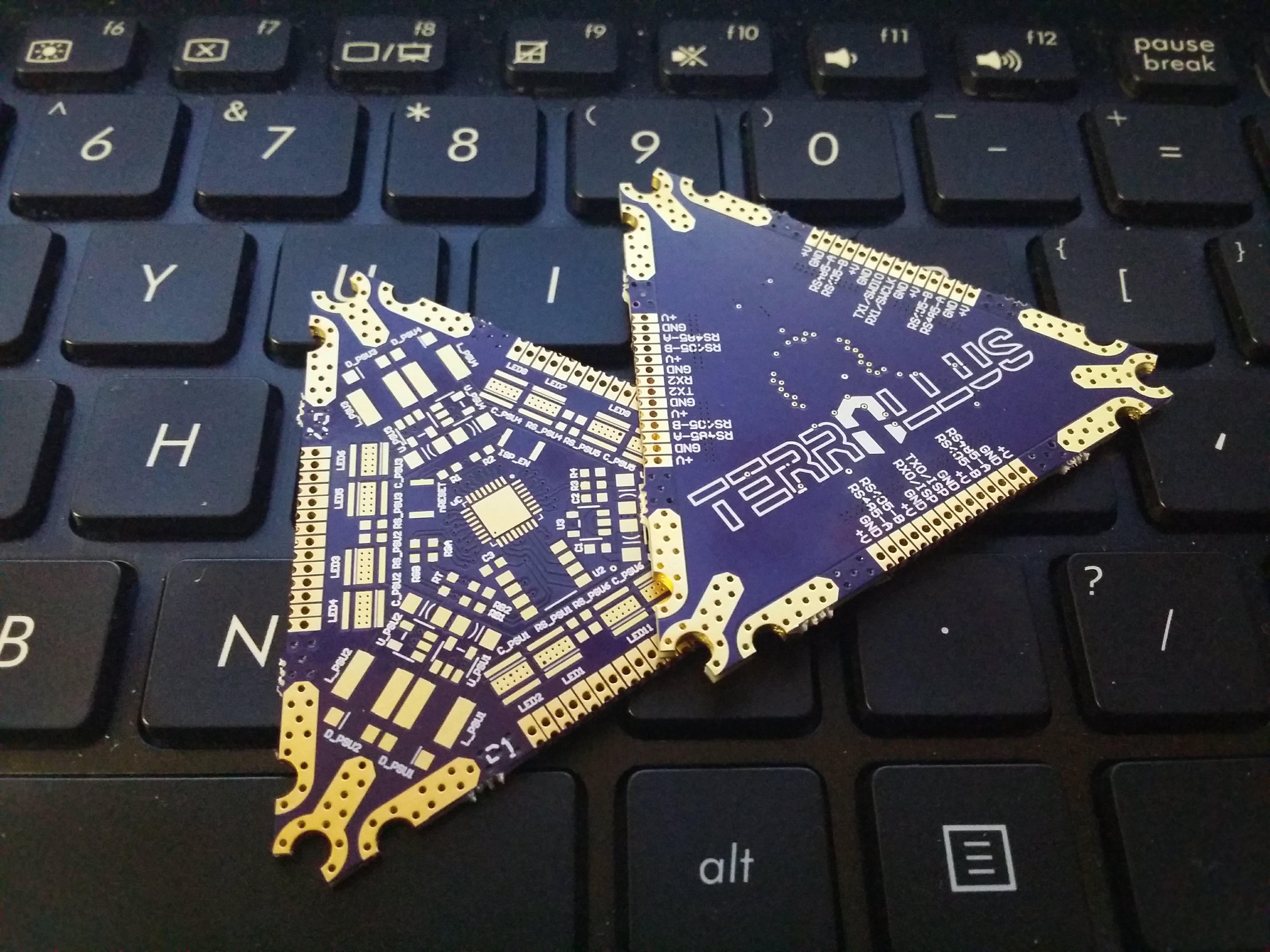
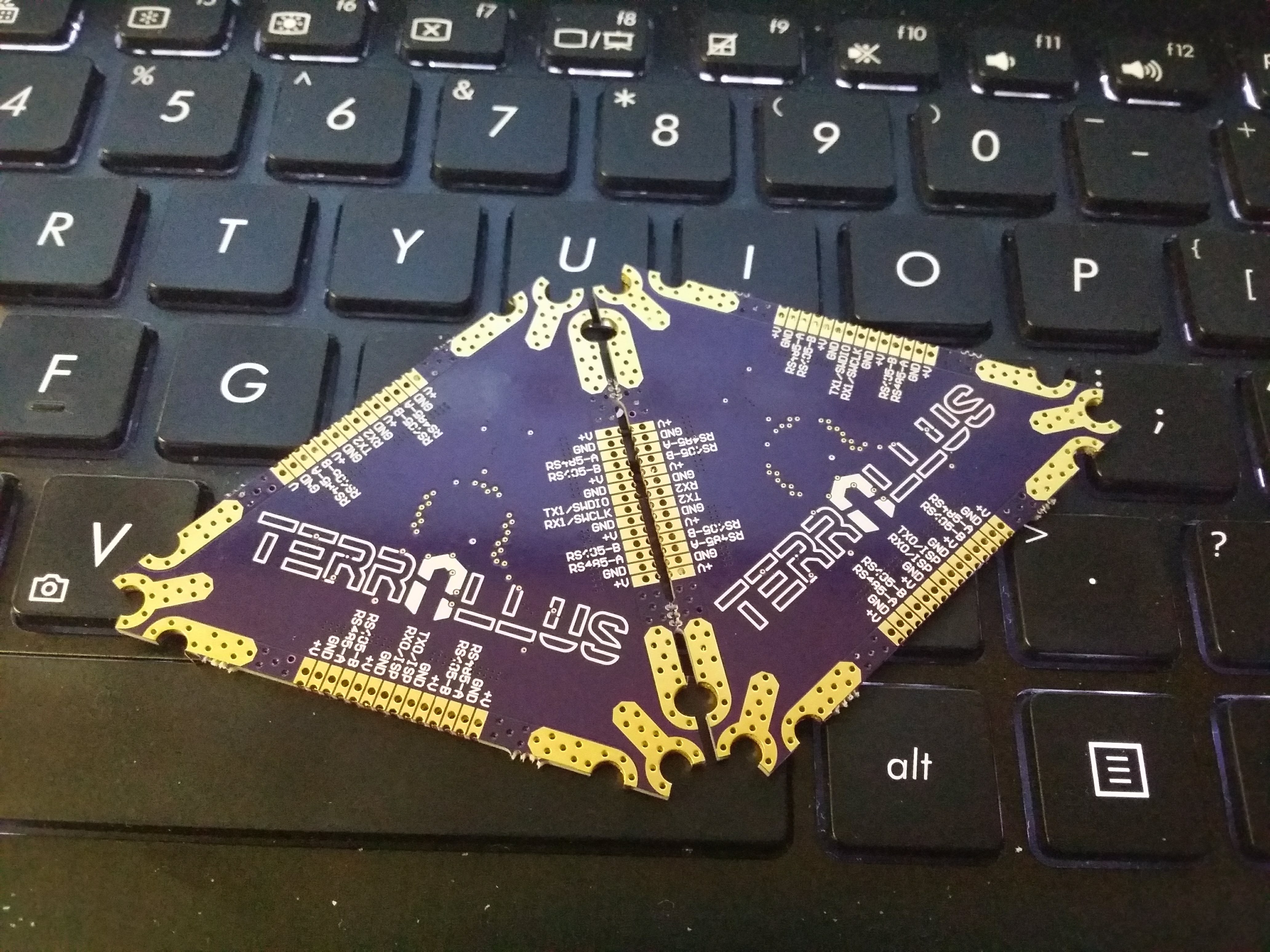
04/14/2018 at 20:50 • 0 commentsSo I wasn't expecting this but I ended up getting both the revised PCB AND the SS solder paste stencil at the same time in the mail!
![]()
I am always interested in seeing how everyone packages their products and I have to say even OSH Stencils did a fabulous job.
![]()
I especially like the caution sticker on the top! The stencil came out real nice and it was definitely worth it. I can't even complain because I don't know of anyone that can beat their price to be honest.
![]()
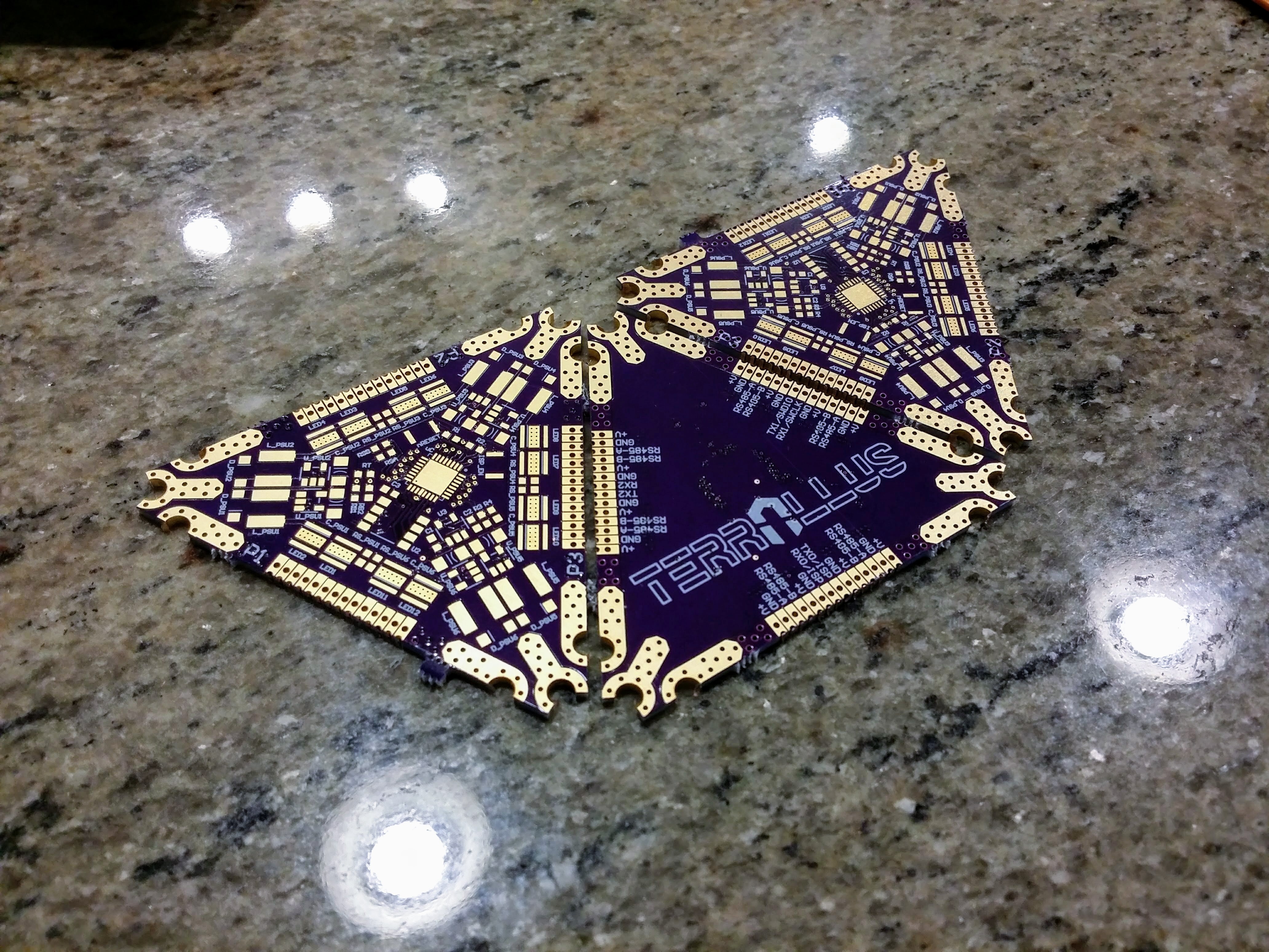
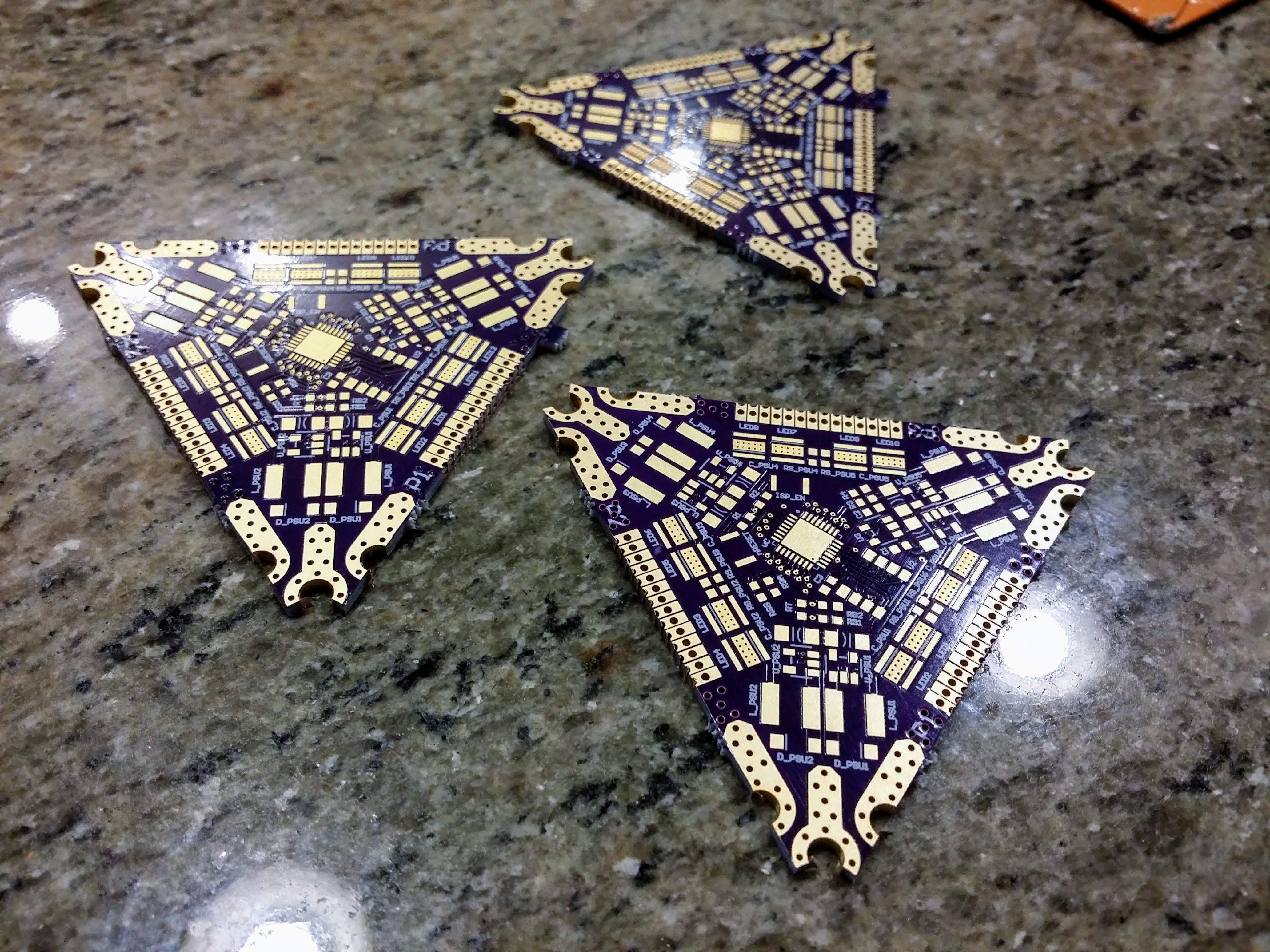
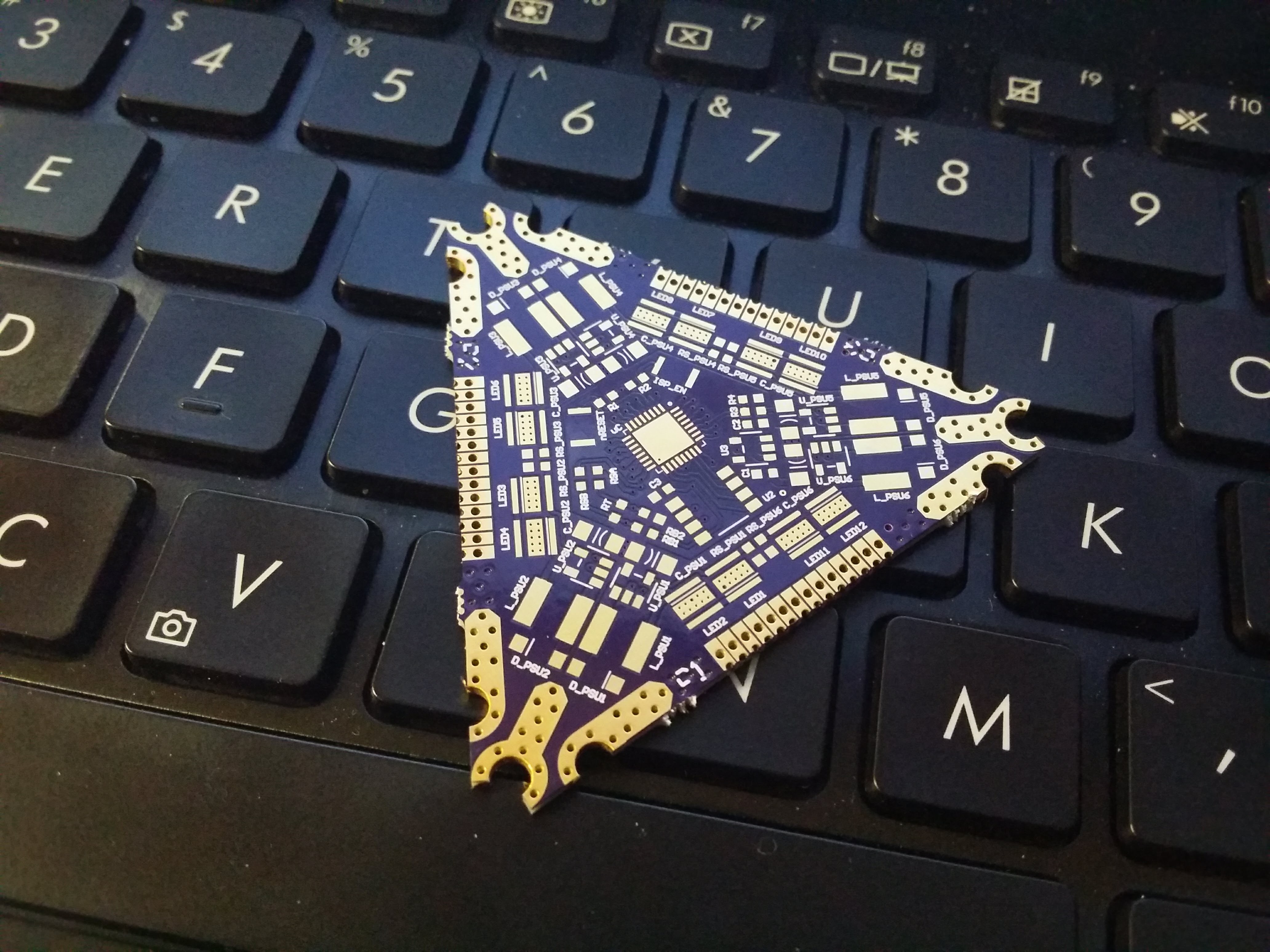
The PCBs of course turned out great and visually there seem to be no issues. I am always surprised at the quality of the silkscreen and how its so crisp looking.
![]()
Overall I am quite happy and can't wait to get this version built - with heatsinks this time!
-
BACKLOG 20180322: First Hot Test
04/06/2018 at 03:05 • 0 commentsReruns received...
I received the reruns from OSH Park and they look beautiful!
![]()
Figure 1: Top side of rerun Top side looks great, just like the previous run.
![]()
Figure 2: Bottom side of rerun And, the back side looks as its supposed too!
![]()
Figure 3: Bottom side IO interface A quick continuity test reveals that all is well and that all the internal layers are intact.
Hot test...
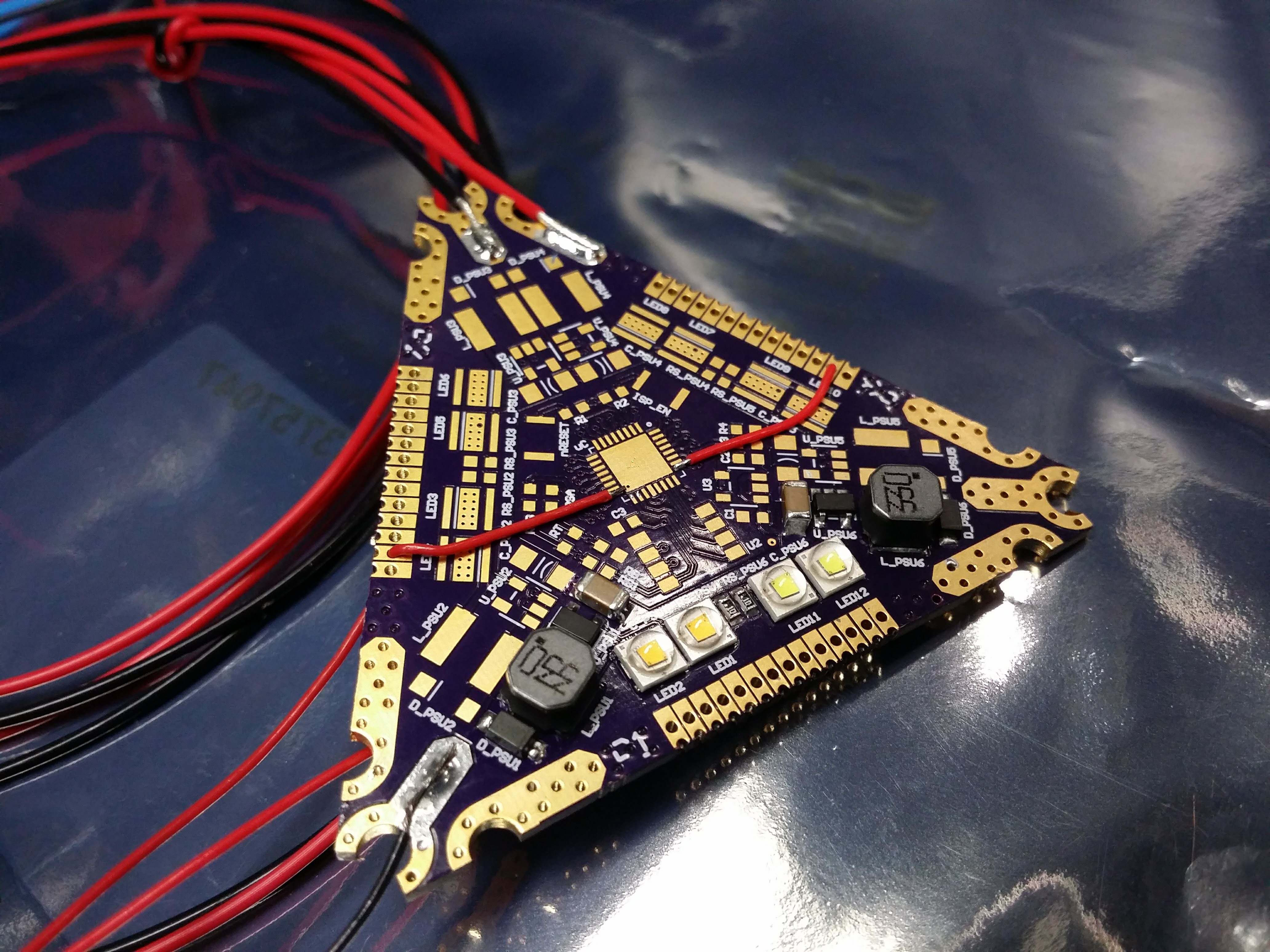
After a quick order on DigiKey, I received the parts and began the reflow soldering of the LEDs and their respective buck converters. The LEDs were the most difficult part because I didn't want to damage the LEDs by using the hot air pencil above them.
![]()
Figure 4: Board populated with 2700K LEDs on left and 5700K LEDs on the right I also ended up just soldering wires to the micro controller pads that are supposed to be the PWM outputs to the buck converter. This way I can test it using another microcontroller board or in my case a function generator.
![]()
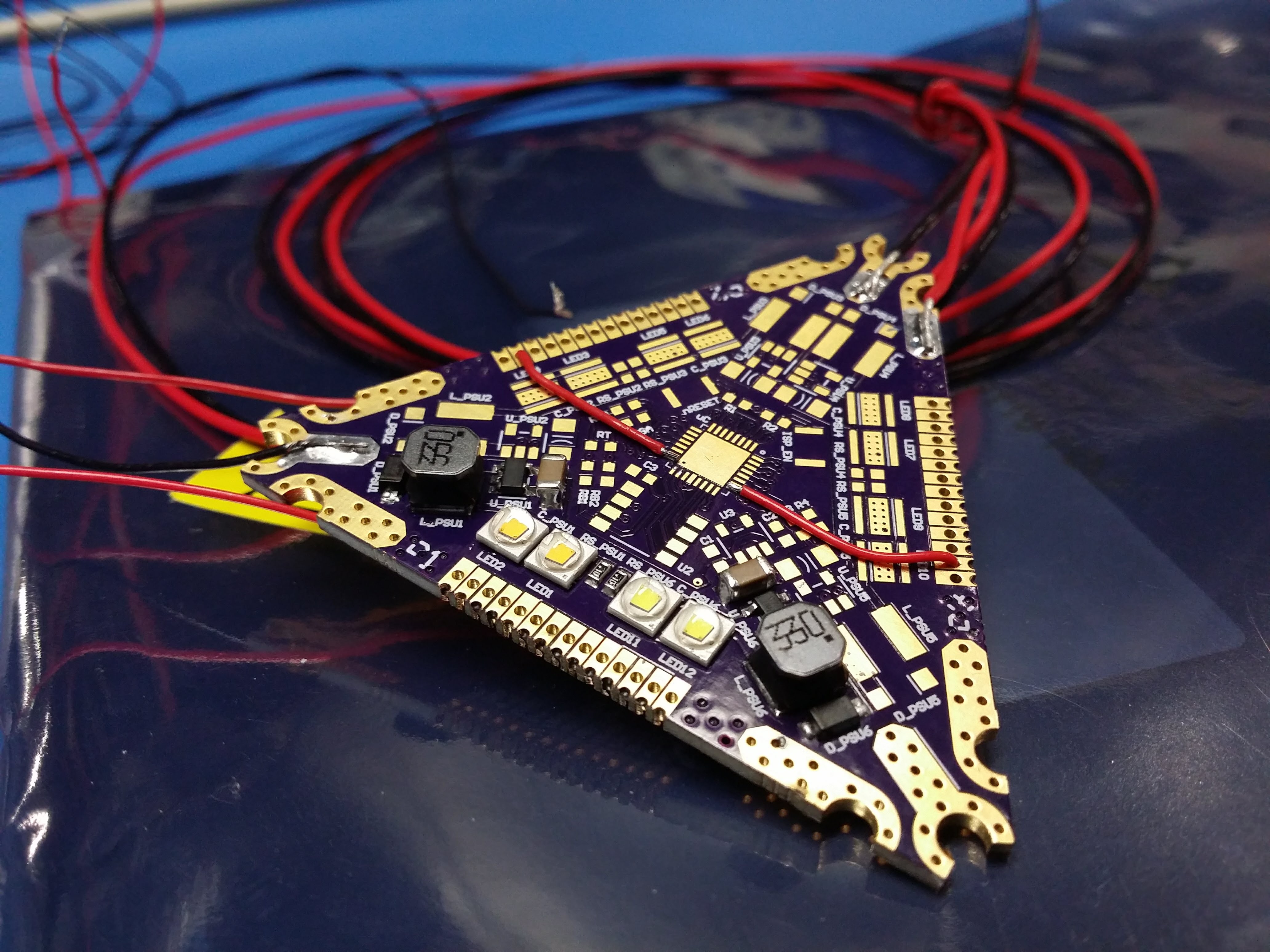
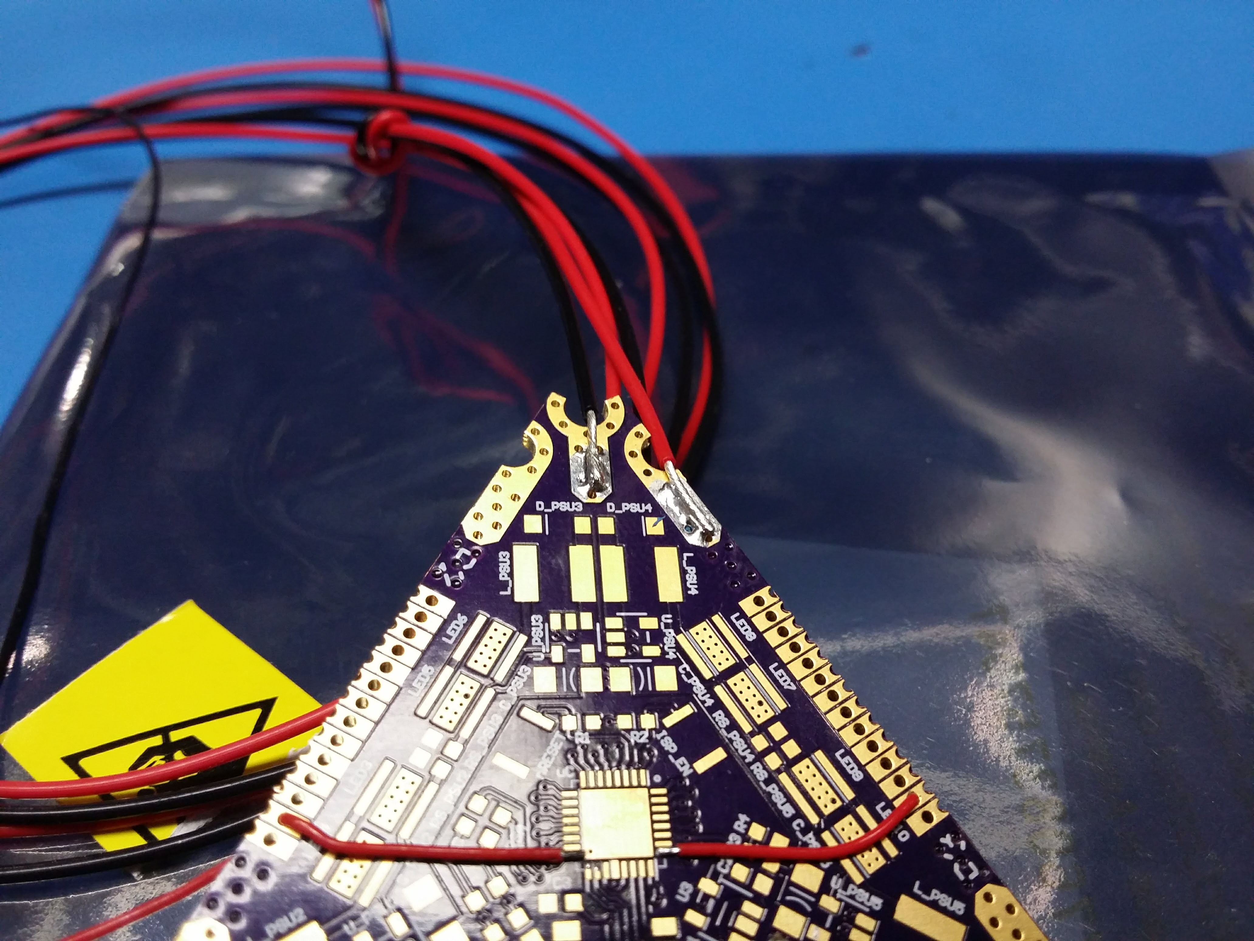
Figure 5: Board all soldered up complete with PWM wires In case it wasn't clear about how to power the board, Figure 6 shows how the screw and wire combination power pads are used.
![]()
Figure 6: Power wires to board Hot problems...
Unfortunately I wasn't able to pictures of the circuit in operation because I ran into some problems. First off, holy crap are these bright! At first I was only able to the the 2700K LEDs working but after a quick reflow to ensure all the LEDs had settled, the 5700K turned on. As bright as they are, they also get hot very quickly, thus I wasn't able to run them long enough to take a picture. This heat was somewhat manageable at a PWM duty cycle of 20% @ 100Hz but even then I could only run them for no more than 10 seconds. I suppose the next order of business is to look at heat sinking and some temperature measurements.
Some quick measurements confirmed that the LEDs are consuming just under 6W per pair. Each cell has 6 pairs of LEDs so that means I am going to have enough heat to desolder the LEDs. Fun...
Then I did the stupid thing... I increased the supply voltage up to 24V and then all the LEDs turned off. I went over the reverse bias voltage causing them to short for a fraction of a second and then fail in the open. I have already made the necessary changes to the BOM so that all components can withstand the rated 40V input.
As an aside, while I was troubleshooting what happened to the diodes, I came across a PCB layout error. The footprint of the LDO linear regulator used for the microcontroller power was incorrect. I switched a couple of pins around probably when I was looking at some other part. In any case, the issue has been resolved, new gerbers were produced with the corrections recommended by OSH Park and they should be on their way to me soon. I also ordered a stencil from OSH Stencil so that should be exciting... -
BACKLOG 20180202: PCB Issues & Fixes
04/05/2018 at 02:09 • 0 commentsI Did This To Myself...
So I placed an order with OSH Park for the PCBs on January 13th and I wasn't expecting them to be here so soon!

Figure 1: 1st cell prototype 
Figure 2: 1st cell prototype backside The silkscreen turned out fabulous; the soldermask and hole registrations are VERY good. And then I noticed something...
If you look carefully at the soldermask in Figure 2, notice the lack of copper pads where the ground pads and screw pads are. A quick continuity check further confused me as all the IO connections were shorted together along with the power pads on the side and the corner ground pads.
Looking further at Figure 2, you can see that the vias seem raised and bumpy. The same can be said about the power pads and IO connectors. Compared to Figure 1, all seems well on the top side of the board.

Figure 3: cell edge inspection top 
Figure 4: cell edge inspection bottom A quick look under the inspection scope shows a potential problem in the IO connector. Figure 3 shows the top side (LED side) on the left and in focus. Figure 4 shows the bottom side on the right and in focus. The IO pads seem to be connected on the bottom layer and on the top they are isolated as they should be. Also of note are the internal layers visible in both inspection pictures.

Figure 5: cell prototype missing plane It seems that the ground plane on the bottom later is entirely missing (as outlined in Figure 5). However, the IO connector pads are all shorted together. Weird...
The Fix...
I informed OSH Park about the issue and their response was quick and quite unexpectedly detailed. They were so awesome in fact that they dug deep to figure out the problem and over the weekend at that! It turns out it was
partlymy fault although I didn't know it at the time.
Figure 6: cell ground plane over extended The internal planes were initially setup as an equilateral triangle but my board outline cut through them. This meant that there were parts of the planes outside the board as shown in Figure 6 (top portion of plane visible above and past the center "GND" screw pad). When the gerbers were processed by OSH Park, the over extending parts of the plane were removed. However because they are part of the same plane entities, the entire plane was removed and funkiness ensued.
The folks at OSH Park were very thorough in their investigation and offered a very concise explanation in a timely manner. They were nice enough to rerun the boards for me at no cost and even offered expedited shipping!
Thank you OSH Park!
OSH Park, thank you very much for the help. I learned something new and I hope other companies follow your lead...
-
PCB Elements and Features
03/24/2018 at 23:31 • 0 commentsPCB Layout...
There was some back and forth about how many layers the PCB had to be. For keeping things cheap, the obvious choice would have been to use a 2 layer board. However, there needs to be a balance between being cheap and being simple. Sometimes to be simple you have to be a bit "anti-simple". The decision was then made to use a 4 layer board as it has significant benefits:
- Meets size constraint for part placement and routing
- Ample room for thermal management without traces in the way
- Routing got VERY easy
- Gives way for large planes
- Very important in the overall design
- Does not require the need for bus bars or external power distribution. The boards themselves can carry the required current.

Figure 1: Gerber top render 
Figure 2: Gerber bottom render The PCB stack up is as follows:

Figure 3: Gerber top layer render Top Layer
- Contains all the electronic components
- Poured as "+V" to provide a large current path for adjacent cells
Figure 4: Gerber signal layer 2 render Signal Layer 2
- Contains 3.3V distribution and PWM control traces.
- Poured as "+V" to complement the Top Layer plane.
Figure 5: Gerber signal layer 3 render Signal Layer 3
- Contains all RS485 and UART lines interconnecting the 3x edge connectors.
- Poured as "GND" to provide a large current return path as well as thermal distribution plane for the LEDs.
Figure 6: Gerber bottom layer render Bottom Layer
- Poured as "GND" to complement the ground plane in the previous layer as well as a uniform thermal plane for heat sinking.PCB Features...
The PCB has pads attached to the "+V" and "GND" plated M3 screw holes to allow up to 12 AWG wire to be directly soldered. With the help of the large power planes in the board, there is no need to have external power distribution between cells. The pads are identical on the bottom layer and enable various mounting options such as carrier boards, spring contacts, direct wire to board soldering, etc.
The I/O connector is symmetrical in design. It can be used in any orientation with other cells and facilitates the use of wires, flat cables, headers, spring contacts or direct "butt" joints with adjacent cells. Power can either be applied with the screw hole pads or the I/O connector. When assembled as an array, it is recommended to use the screw hole pads for the initial power entry into the array and the I/O connectors within the array.

Figure 7: Power pads -
Cell Size & Shape Justification
03/24/2018 at 01:38 • 0 commentsSo the cell was decided to be an equilateral triangle whose sides measure 62.5 mm... But why?
One of the goals for the MOSAIC LS project is scalability. How do you shape a component that can conform to any application thrown at it, scalable? Why, triangles of course!
... Triangles are forever...A triangle is the most basic enclosed shape that can be formed with the least number of sides, 3 in this case. Its used in graphics to reduce the number of vertices in a mesh while retaining the most detail as well as in structural engineering. With triangles you can assemble them into whatever pseudo shape you want. They can approximate circles, rectangles and its not limited to just 2D shapes. They can approximate spheres , rings, domes, boxes, cylinders, etc.
So that addresses what shape to make the "cell" into - an equilateral triangle which keeps things as symmetrical as possible. But what about its size, how big should it be? Too small and complexity becomes an issue as more are required. Too big and it might hinder certain application constraints such as portability or tight spaces.
... Who said size doesn't matter?...
To address the question about how big to make the triangular cell, first we have to consider what applications the MOSAIC LS cell could be used in. One of the key applications that had a heavy weight on design considerations was solar. Many projects out there use solar as their method of energy collection, storage and usage.

Figure 1: 125mm x 125mm solar cell, one of the most common sizes. After a few deep dives on the 'webz, some querying around work and physically measuring dimensions of cells in solar panel assemblies, a conclusion was reached. The most common size of solar cells (monocrystalline or polycrystalline) was a pseudo-square cut from a 160mm diameter ingot of silicon. It measures 125mm x 125mm with corners of 160mm diameter. See Figure 1 above.
If a cell were to be designed with the sides of the triangle measuring 125mm, then one would be left with 1/2 the solar cell uncovered. However if a circle with a diameter of 125mm is considered, it will cover approximately 75% of the cell. The best approximation of a circle using the least amount of triangles is a hexagon. That means there are 6 equilateral triangles whose sides measure 62.5mm in length. See Figure 2 below.

Figure 2: Hexagon made from 62.5mm equilateral triangle Lets see that hexagon with the actual cell PCB outline (Figure 3)

Figure 3: PCB cell hexagon solar cell A near perfect fit with just enough room to add some switching circuitry to boost the cell voltage and to hide a beefy battery behind the hexagon assembly.
... The Goldilocks Principle...
When you consider that particular dimension, 62.5mm, that's 2.461 inches which is just enough to design an enclosure whose outside dimensions don't exceed 2.5". Its small enough for portable applications as a single unit or in pairs/triplets. It's just big enough to be used in large numbers without adding too much complexity and does not exceed the available MODBUS addresses (254) to comprise a 1m x 1m array. Among many other things, it all works out!
Not too big... Not too small... Just right.
M.O.S.A.I.C. LS
Modular Open Source Adjustable Intelligent Control Lighting System