 Yann Guidon / YGDES
I have not yet really started and I already encounter a "little problem".
I chose complementary MOSFET technology (BS170 and BS250, and their SOT23 equivalents) instead of N-MOS ("all those pull-up resistor waste so much power !") but however I move things around, a "simple" D-FF (for a clean, synchronously clocked design) seems to require no less than 24 transistors.
What ???
How many transistors will this clock use ? There will be several Johnson counters so the size will explode !
Unlike classic CMOS digital circuits, which use N-FET and P-FET, the discrete MOSFET transistors have this nagging little parasitic diode, which prevents the construction of proper pass-gates. A CMOS pass gate just needs one N-FET and one P-FET, but MOSFETs must be doubled and connected head-to-head to cancel each other's parasitic diode. This precludes certain classical topologies that save transistors here and there in common CMOS chips.
- (I'm too lazy to draw something clean and too shameful to show my dirty sketches so I'll use online resources.
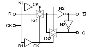
One example is shown there: http://www.learnabout-electronics.org/Digital/dig55.php![]() Another page covers a lot of common clocking problems there http://ece-research.unm.edu/jimp/vlsi/slides/chap5_2.html)
Another page covers a lot of common clocking problems there http://ece-research.unm.edu/jimp/vlsi/slides/chap5_2.html)
 Another page covers a lot of common clocking problems there
 Let's count the transistors: 2 pass gates (noted TG)= 2×4 MOSFETs, plus 2 inverters (2 MOSFETs each) : 12 transistors. If we want to implement a master-slave latch gate with this system, that's 2×12=24.
Let's now look at a simple latching gate : connect two inverters back to back. That's just 2×2=4 MOSFETs, sweet. This can be turned into a RS latch (bistable) with the trick presented in a #DYPLED log there : https://hackaday.io/project/8693-dypled/log/28851-a-dumb-bistable Ignore the LEDs and replace the push buttons with N-FETs and you get a nice little bistable with 6 FET:
It relies on the overriding of an input with another output, protected by a resistor. Without this resistor, there would be a transient direct connexion of the VDD and VSS through the 2 passing transistors (high-side P and overriding low-side N). The resistor trick is "OK" (power is wasted only very shortly because the latch stabilises in a few nanoseconds) but it moves all the complexity to the R and S signals generation, which in turns depends on the clock input...
A NAND or NOR gate requires 2 P-FET and 2 N-FET (as much as the bistable element). A transparent D-latch requires 2 NAND (for driving the R and S lines) as well as the 4 FET of the bistable cell, plus 2 FET for overriding the S and R lines. That's 14 FET and I haven't counted the clock's inverter (which can be shared among many gates).
Now, let's try a "pure logic" approach: build the logic function and translate it into FET topologies.
A MUX2 is made of a couple of NAND2 and a NOR2, that's 3×4=12 transistors. Multiply by 2 for an edge-triggered latch and again we find 24.
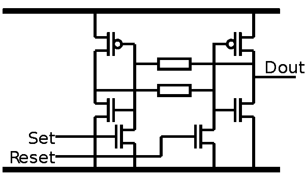
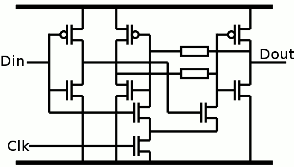
Going back to the previous "overriding" RS circuit, I realise that the control NANDs don't need to be "purely logic". The R and S ANDs can be "computed" by series transistors, instead of just one low-side transistor. This creates the following circuit:
The clock only needs one phase, though the input data requires a complementing inverter. The latch is now only 10 transistors. We're finally getting somewhere :-)
Wait, ...
The low-side CLK N-FET is redundant... The parasitic diode could disturb the circuit but since it is bistable, there should be no actual condition of metastability. And the diodes are in opposing directions so nothing should happen if the the low-side CLK FET is not active.
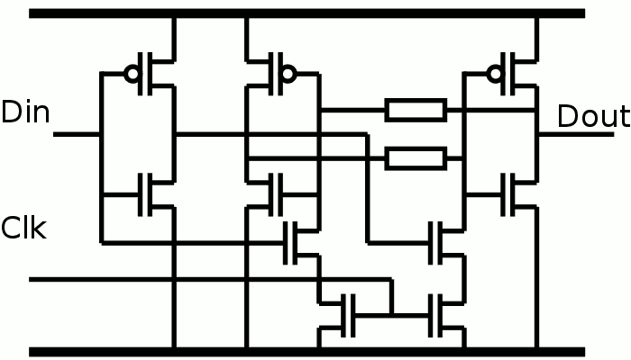
What about a FF ? One inverter is saved because the latching loop provides complementary data Q and /Q. This is amazing because a Johnson counter is made of shift registers so there will be 7×2=14 transistor per stage, instead of 24. And since the data pairs are complementary, the reversing/inverting stage only has to swap Q and /Q !
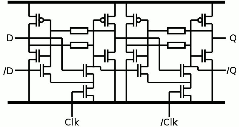
For good measure, add one P-FET to each bit for a proper reset.
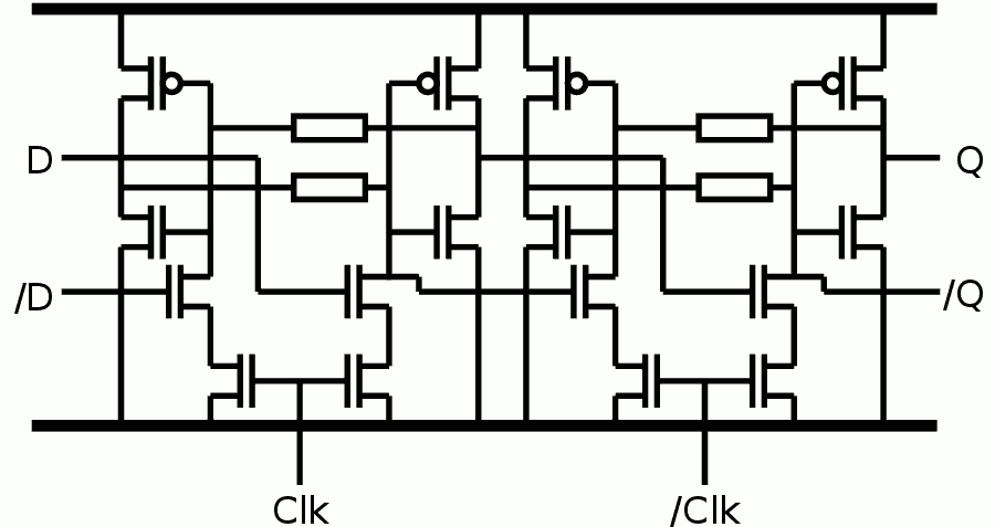
Of course, this circuit is NOT TESTED (yet)OK, I was wrong about the redundant CLK N-FET. In an ASIC it would be true but with MOSFETs, the parasitic diode makes one bad case possible (I overlooked it). This gives the following circuit with 8 transistors:
Ideally, Clk and /Clk must not overlap so a 4-phases clocking system would be nice. In practice, I wonder how the parasitic capacitance of the gates will affect the system. For a clock divider, it is pretty obvious that, depending on the state of the DFF, Q will change before /Q and the reverse will happen again for the next cycle. An inverter seems to be needed to properly drive the clock lines...
Discussions
Become a Hackaday.io Member
Create an account to leave a comment. Already have an account? Log In.