Ted Yapo
-
IC die images sans acid
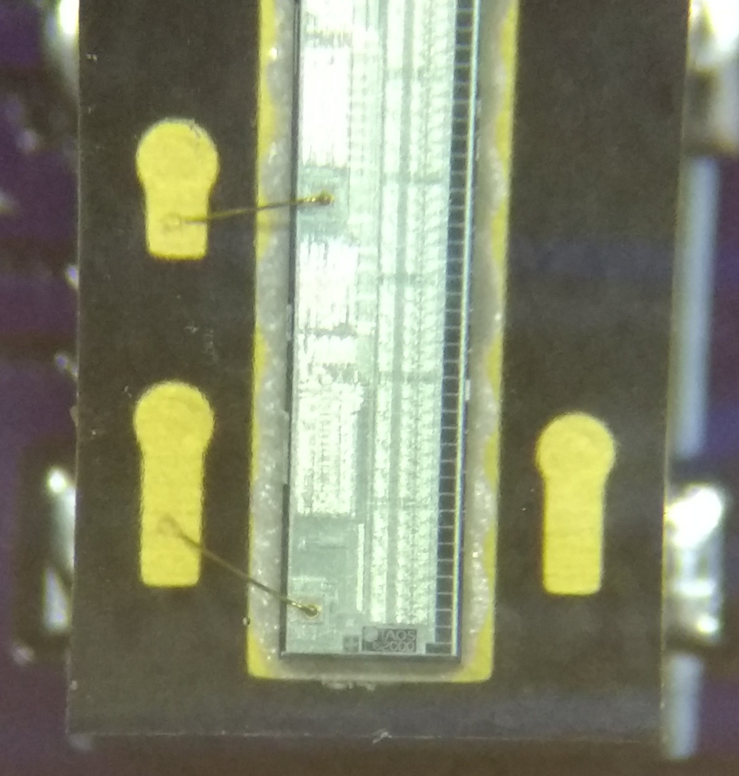
04/04/2018 at 03:20 • 0 commentsIt's easy when the package is transparent! In this case, a linear image sensor. After mounting it on the PCB, I put it under the microscope to check the solder joints, and was pleasantly surprised to see the pixels themselves. That's them on the right. The end one is a different size/shape than the others.
![]()
You can also make out the text "TAOS C 2000". Copyright markings on the chip, nice. I don't see an open-source license on there, though :-(
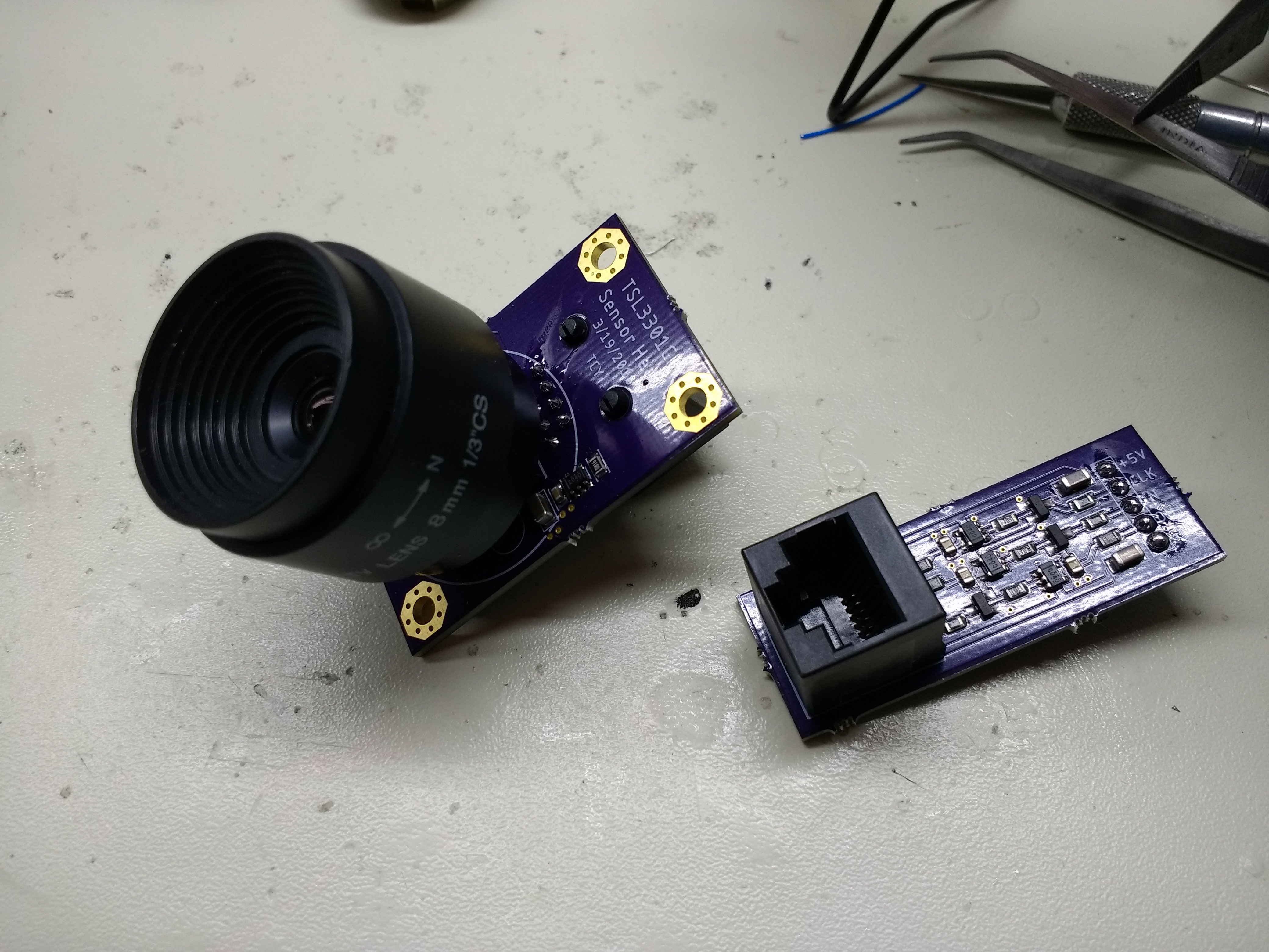
I also built the matching receiver PCB, and assembled the CS lens mount on the sensor board. I just need to connect them with an ethernet cable and - nothing - I didn't write a driver for this thing yet.
![]()
So, I have to get into a software mindset and crank out some code. I'm just not feeling it tonight. But the hardware is done, so yay!
-
Receiver PCB
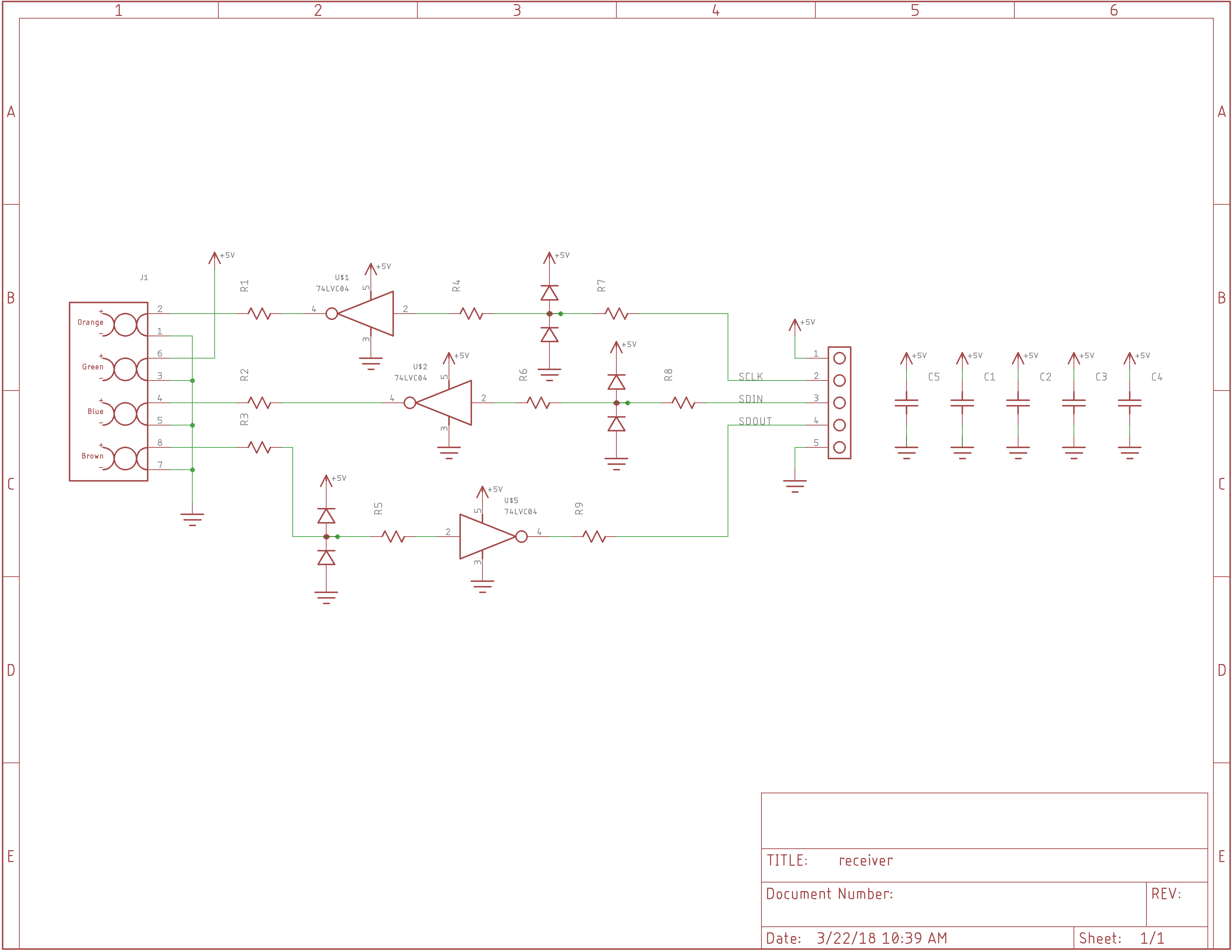
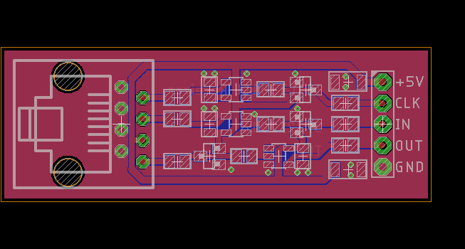
03/22/2018 at 15:01 • 0 commentsI was originally going to integrate the MCU, stepper drive, and everything else on one PCB, but I decided to go modular, so I can just wire up some existing boards for a prototype. The missing piece was a driver and receiver for the MCU end of the cable, so I threw together a little PCB for it.
![]()
It uses 74LVC1G04's as cable drivers and receivers, with added parts for ESD protection. The connection to the sensor head is over a cheap ethernet cable. The PCB was really straightforward to route.
![]()
I wish they were all this easy.
Now that I sent it out, I regret not adding mounting holes. Oh, well, it costs less this way.
I also should have routed the 5V line around the ground pins on the RG45 connector instead of between them, considering the signal return paths. There's a ground plane underneath, but it would probably help to keep the top plane unbroken there.
-
"Toy" Sensor Head
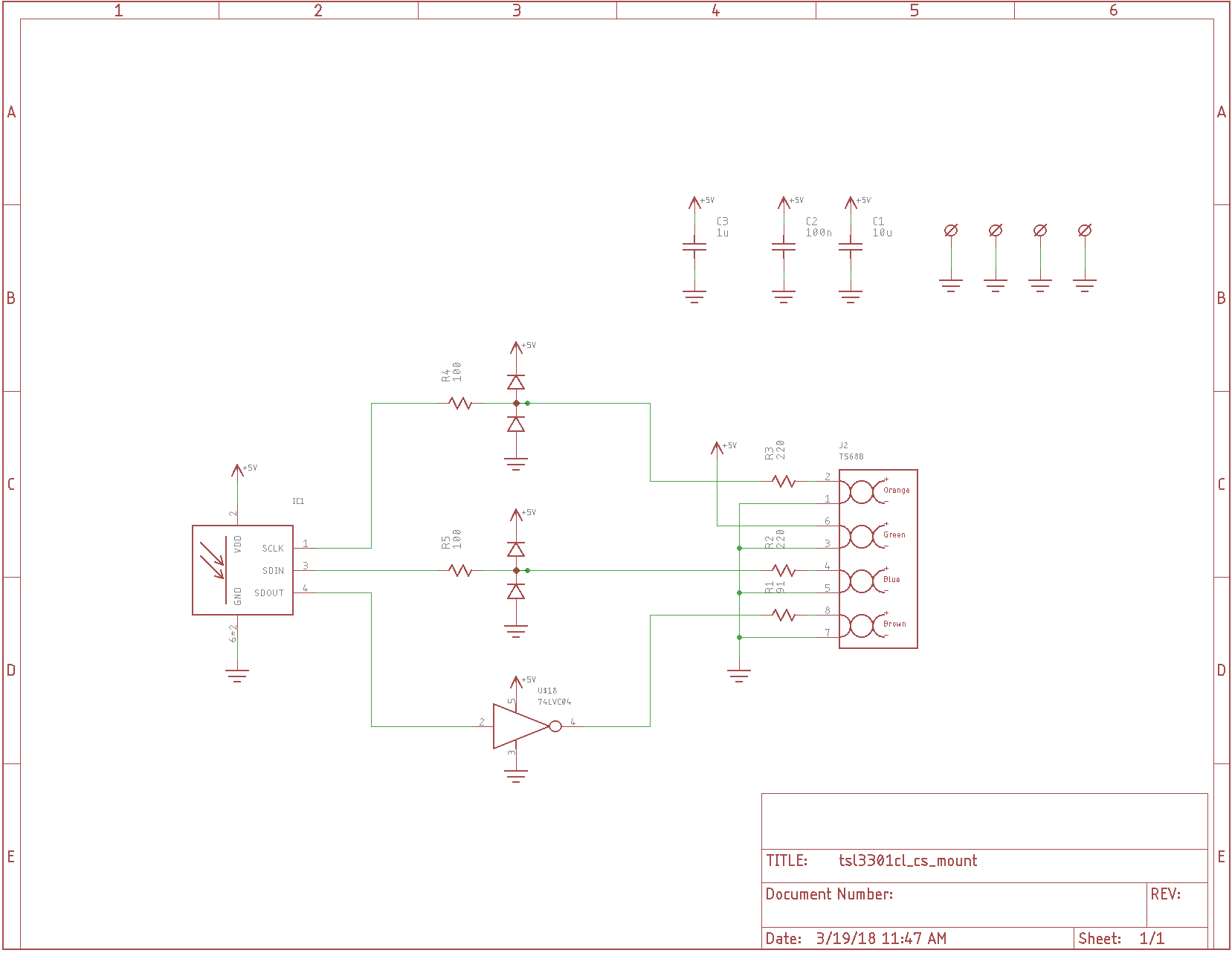
03/19/2018 at 17:15 • 0 commentsI designed the first pass of a toy pushbroom image sensor. This should get me started, anyway. The sensor is a TSL3301CL, with 100x1 pixels, 77x85 microns each (centered on 85 micron centers). These are big pixels, so noise will be low, even if the resolution is poor. The circuit is really just a breakout for the sensor:
![]()
The diode/resistor networks on the sensor input lines are there for ESD protection. The inverter is used as a cable driver, and with the 91-ohm series termination, should give a good match to 100-ohm twisted pair. I'm using ethernet jacks and cabling because they're cheap and plentiful. Twisted pair and controlled impedance is a huge plus, too.
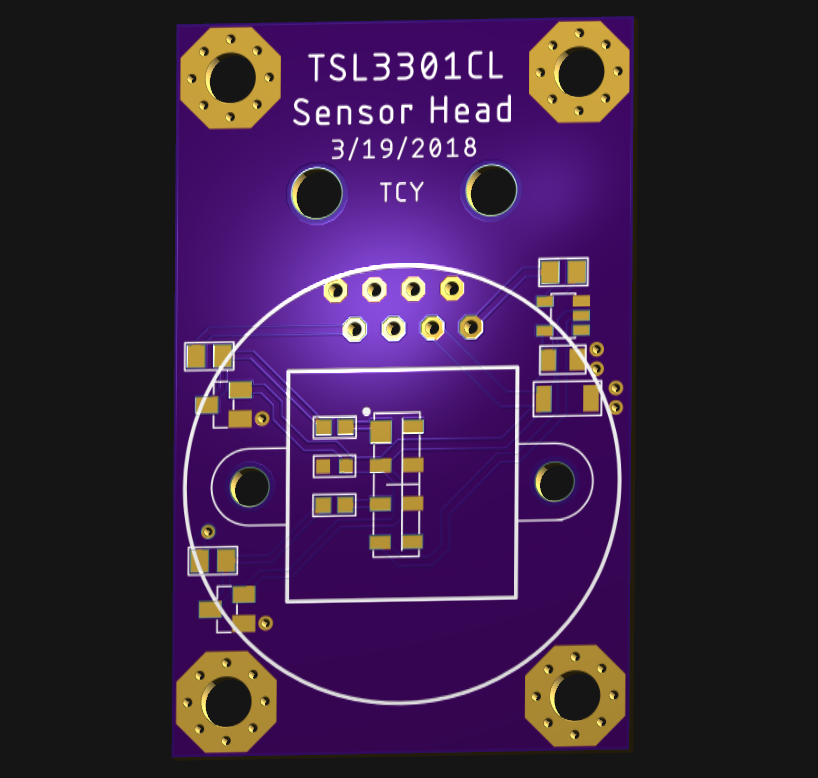
The front of the PCB has most of the components, including the sensor and a metal mount for a CS lens.
![]()
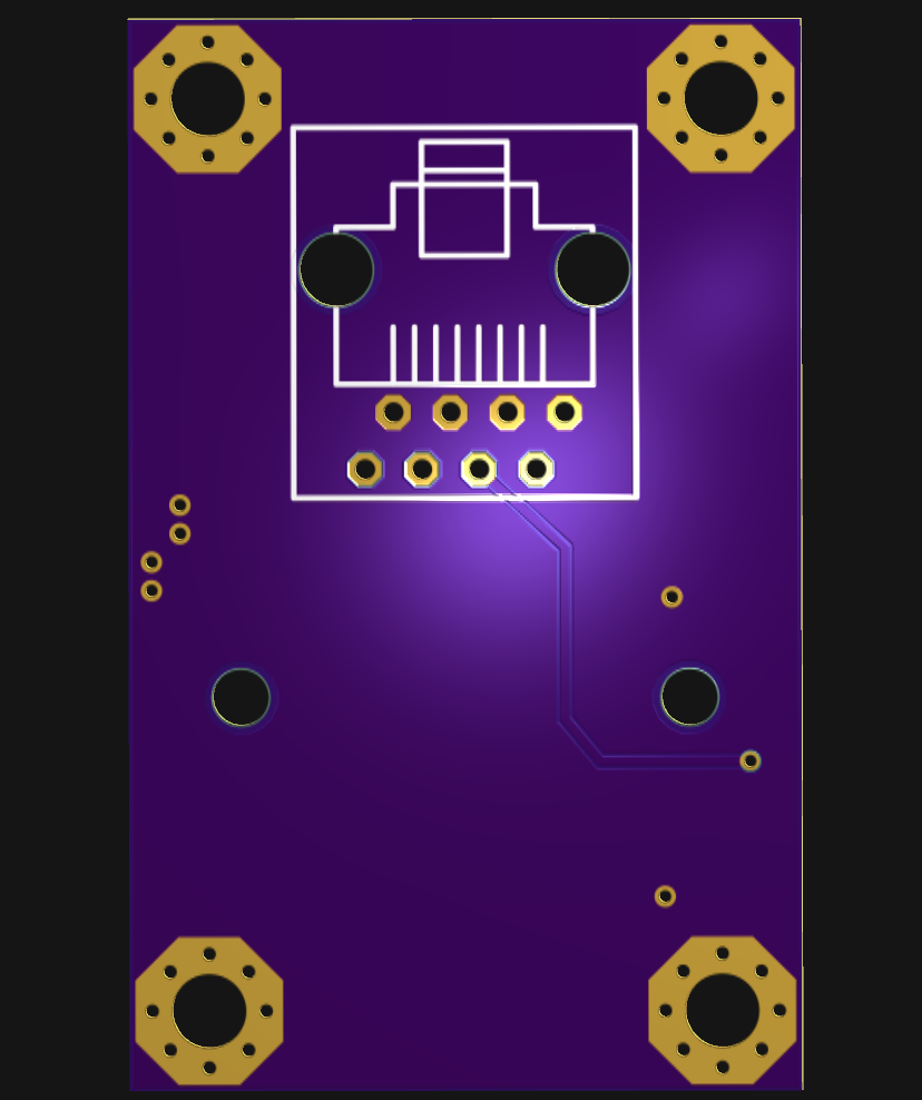
The back of the PCB has the 8P8C jack:
![]()
It's all very straightforward. Now, I have to design the other side. A microcontroller, stepper driver, and a big flash memory to store images is probably all that's required.
Depending on how thick the solder ends up when I reflow the senor on the PCB, the flange distance may be a little short (I think about 0.35mm). This is much easier to fix (by inserting a shim) than one that is too long. I'll have to test it out once I have all the parts.
At first I thought that focusing would be difficult, but I think I can just image any sharp black/white edge and probably focus by eye.