Michael O'Brien
-
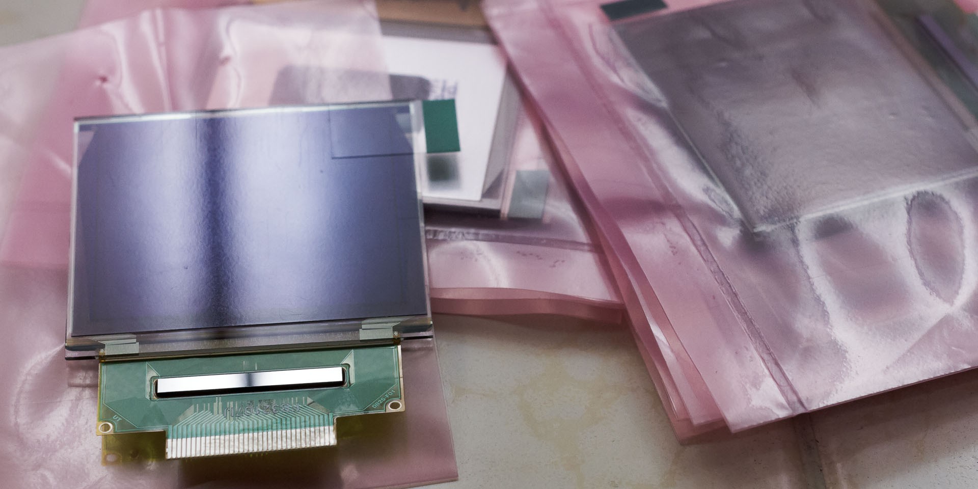
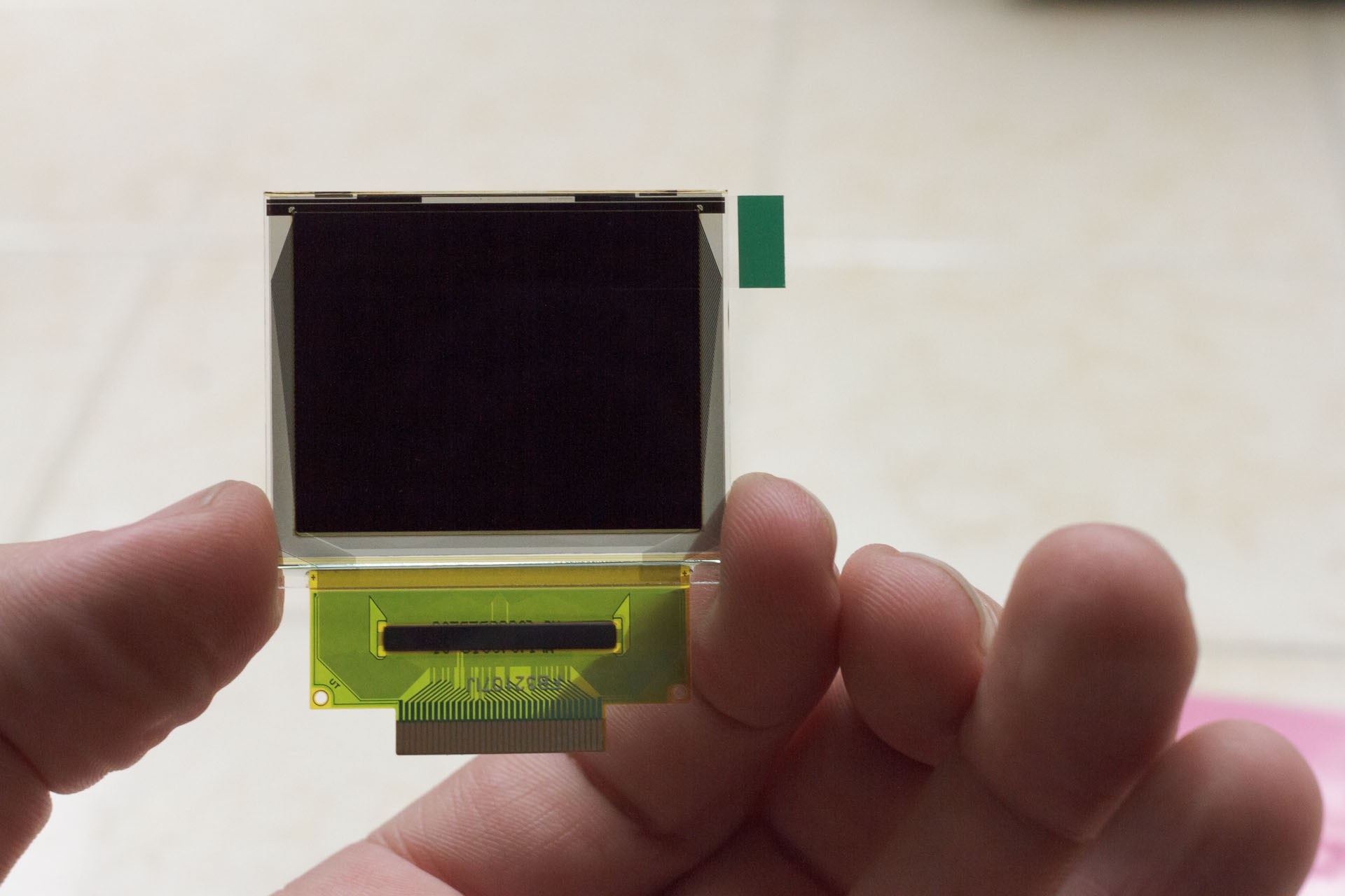
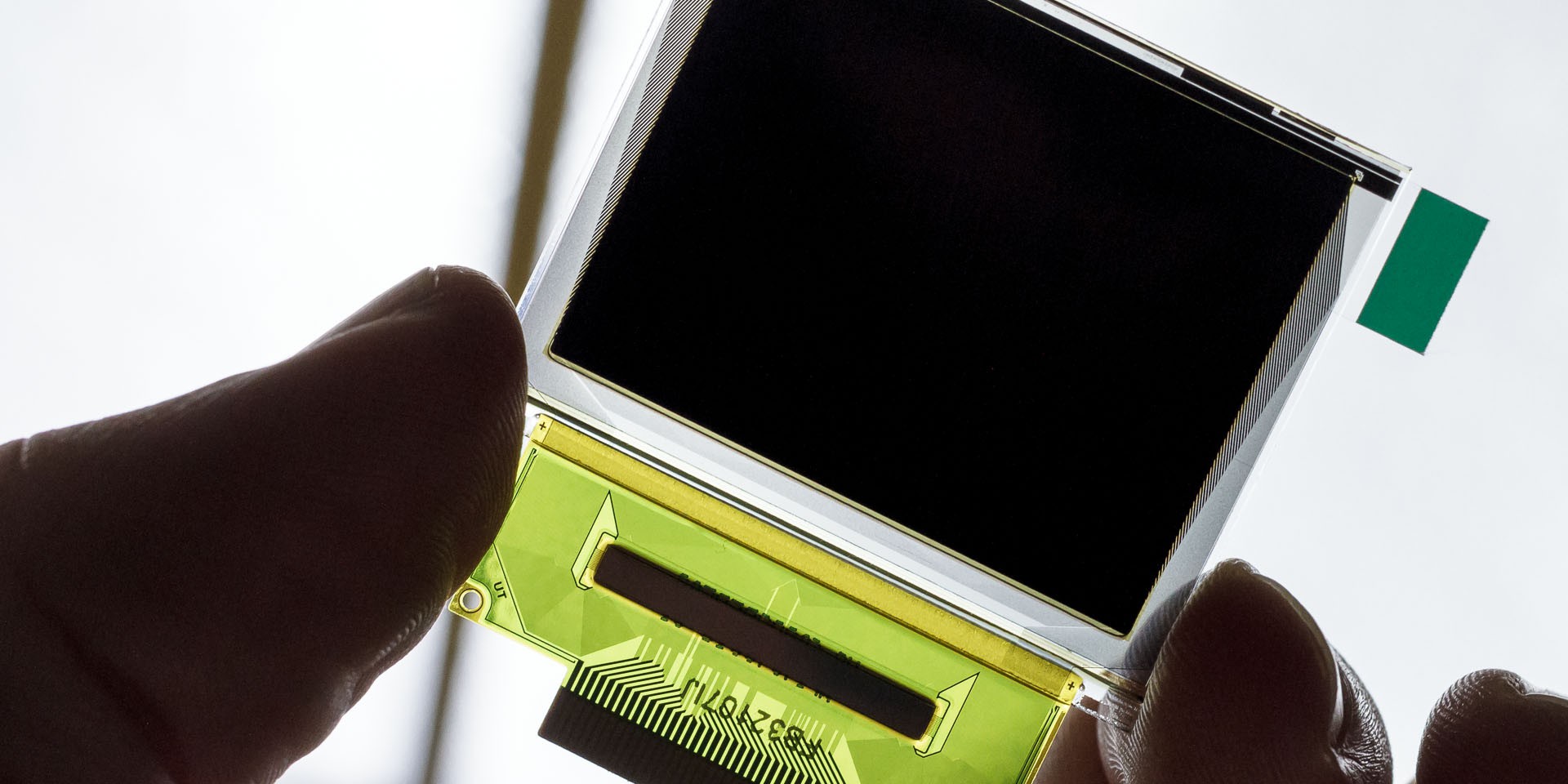
Displays Arrived!
05/20/2014 at 03:52 • 0 commentsI hope to have the board for supporting them ready for a lab sometime tomorrow. The board has some logic integrated with PWM, buttons, terminations, and even some board-to-board stuff since there are no easily accessible perpendicular mDP/Thunderbolt receptacles :/
Anyhow, picture time:
![]()
![]()
![]()
-
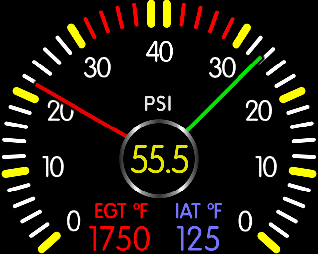
Displays aka Gauge Faces
05/15/2014 at 07:41 • 0 commentsFirst a little history...
The original Doniol gauge used a 128x128 OLED screen. I knew I needed something larger so I looked around and found out the most readily available larger OLED was a 128x160 screen. These are available with 2 different display drivers: SSD1353 and the SEPS525, the latter of which is more prevalent as far as I can tell. I've found smaller versions than what I needed, bigger brothers, and cousins. They are all functionally the same I assume as the data sheets give the physical specs of the displays as near identical.
I ended up stumbling across this one. Though inexpensive, I was told that the lead time was 12-14 weeks. I bit the bullet and bought 8, as I already had a small one for early testing, to give me 3 D-DAQs with 3 gauges 5 days before the contest was announced. Well, today I got a shipping email from Future Electronics so I'll be getting them [a lot] sooner than expected!
Now, I know a 128x160 screen is a bit small. but ~1.7" is the largest display diagonal this pixel count comes in with this driver. I also figured that at some point in time, I'd want the graphics to fit on a larger screen or differently proportioned. I made up a spreadsheet that did the auto-adjusted the needle sweep in degrees for the display dimensions, spit out X-Y coordinates, degrees, and accuracy errors for each tick mark of gauge faces. I was toying with the idea of doing the line drawing myself, and having them antialiased, but have since decided upon rendering sprites onscreen instead. This was relatively simple as I was using the spreadsheet and Photoshop for mockups...
Illustrator would probably be better to make this in as it'd be resolution independent and if I ever changed displays, it'd be an easy adjustment, but I'm a raster guy and I also knew a little bit about Smart Objects. Each tick mark, big or small, is a SO. In fact, all of the white ones are linked to each other so if I change the dimensions/color/shape on one, they *all* change. Same for the larger yellow and small red ones. This makes a global scheme change a very simple task. I generated the file at 4x the display resolution so I could down sample any rounded trig errors from Photoshop and just went to town. There are nested groups and currently 565 layers, but that's increase as I'm doing more layouts. As a compressed TIFF with flat color, the image file is over 90 MB.
Text alignment was tricky as the fonts are not monospaced. I ended up with a smart object like the tick marks, rotated the text appropriate for it's screen placement, and then rotated the smart object the opposite direction (with it's anchor in the center). If I needed the text closer to the ticks, just move it up and save the smart object instead of having to compute the trig for x-y coordinates and the offset for text width and adjusting things to a floating point pixel ;). Overall it's a lot of work, but it's for future proofing the design.
One such example for the details in this setup is that it allowed me to easily tweak the existing format and create a split gauge setup for monitoring 2 turbos, or boost an exhaust manifold pressure for VNT/VGT turbo tuning:
![]()
This brings me to a point a few may be asking. Isn't a 1.7" display a bit small? Yeah, it very much can be. Especially if it is mounted too far from the user. Now, because I'm driving the displays directly via SPI, going larger means I'd have to use a lower frame rate and that is highly undesirable. Well, SPI is just a protocol. These displays usually can be driven off of a 16-bit or 8-bit parallel interface. Well, as I mentioned before I can code the buttons for the user interface can act as a a 3-bit address. Instead of making them have an initial low/high pull down/up, I can choose NO or NC buttons. Tack on a microcontroller to be an SPI slave, have D-DAQ send the equivalent of drawing commands instead of RGB pixel info, and make sure the slave micro is fast enough to drive the new display at a high frame rate via its parallel interface, and these displays can be large enough to fulfill the user's desire. Or at least within some reason for mounting in a car and drawing power from D-DAQ.
-
Prototype 2?
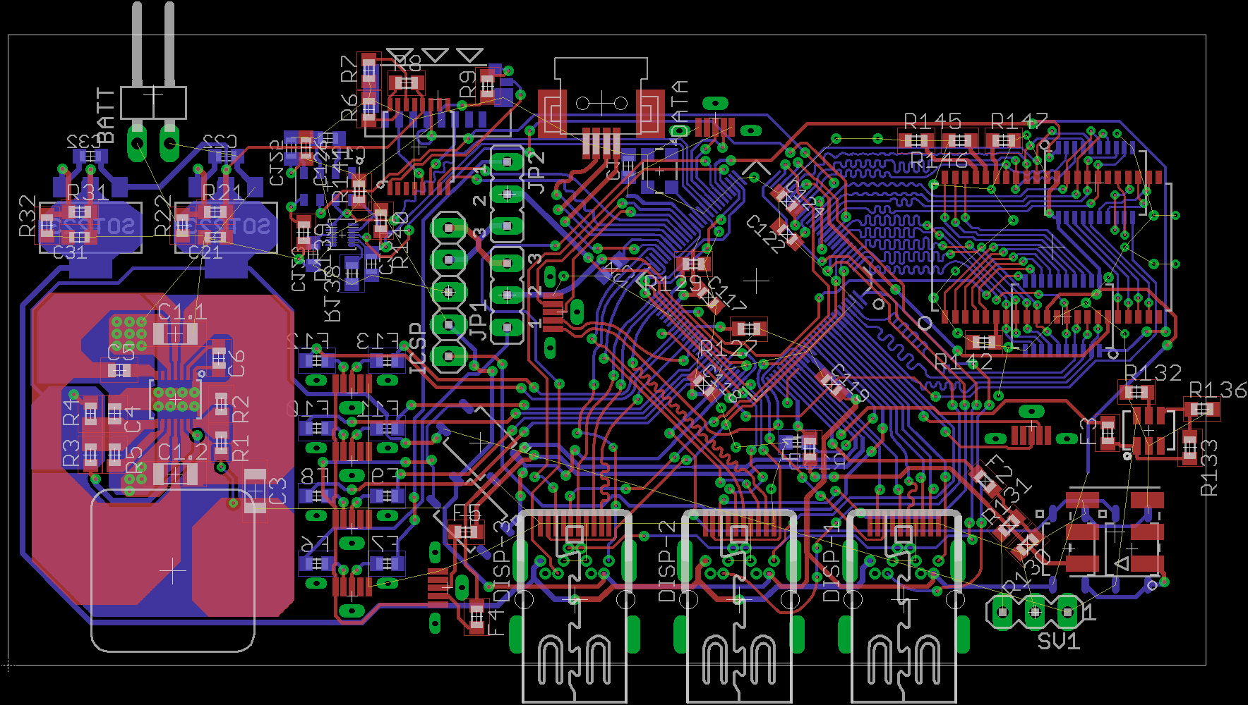
05/12/2014 at 07:06 • 3 commentsWent back to the board layout as I noticed a couple things after sleeping on it for two days. 14V supply was running next to the switching plane for 3.3V so I'm expecting it to be a bit noisy, but I can filter that out if it's too much. Next up I went around my tight areas with a bunch of criss-crossing around the mDP female plugs. Adjusted some trace spacing and fixed a couple things I was unaware of initially. End result were the extension of a few ground planes without the need of vias.
Last night while looking around on a couple other sites for pricing, I noted that my board is <5 cm tall and <10 cm wide. A 5 cm x 10 cm board is apparently common for prototyping. Learn something new every day. Found another shop that can produce prototype boards a bit more quickly and with an e-test. I decided to up my board's size a bit to fill this area. I did so 'cause I only had 2 holes for mounting and figured 9 extra mm would space me for the other 2.
I changed the order of the main pressure sensor, EGT connection, and aux pressure sensor, centered the components inside the new dimensions and proceeded with similar cleanup to what I listed above. Dropped off 8 vias, added the mount holes and I'm now at 454 drills on the whole board, aka ~59 per sq. in.. It'll double manufacturing cost, but I'm sure I can half that number or decrease it even more than that if I bumped over to a 4-layer board.
Either way, I'll be ready to test and adjust the layout once I get the Osh Park boards and have at 'em in a few weeks.
Edit: Speaking of which, I ran the numbers for the LDO's temperature requirements and wow, I would burn up the 14V rail pretty quickly. Due to it's load and being driven by the 5V rail, I had to adjust a couple things for thermal dissipation. I've also switched it up to drive the 14V rail from the power for the whole board, not chaining it from the 5V output. Not sure if how I'll do this, but if I have a greater load on the 14 rail in the future, I will need a new LDO as it's not strong enough for more than ~250 mA.
-
OshPark to start with
05/10/2014 at 03:21 • 0 commentsSo, I'm initially going with OshPark for the prototype boards. I'm close to their tolerances, but 3 boards is about 1/3rd the cost over 4pcb. If they reject the boards for too much details or too many problems, then I'll fall back to 4pcb. Upon batch production, I'll be going with them as their per unit cost is hard to beat.
The downtime of having OshPark produce them gives me a window to create the PCBs for the display and initial sensor boards due to their size and relative inexpensive, I probably have 4pcb produce them so I'll get them at the same time my mainboard will arrive. Also, I can electrically my one-offs from OshPark to see what their precision and QC is like at this level of detail.
Oh, and I love the output from FreeDFM:
![]()
Edit: I shouldn't forget that I still have to finish rasterizing fonts and separate out various graphical elements in order to produce the GUI in software. The firmware on D-DAQ is my next big hurdle and having a breather while the board is produced is useful ;).
-
Prototype Board on File
05/09/2014 at 20:40 • 0 comments4pcb has my files and I sent them to OshPark as well, which you probably gathered from the new photos. I noticed that there is some banding withe the copper layers and I'll look into that later. I also submitted the same CAD files to 4pcb's FreeDFM site and I'm waiting for an email response. The files clear with a 7 mil tolerence, but since that is so close to 6, I'm wondering if 4pcb will be better. The board is highly dense too weighing in at 460 drills in the 7.25 sq. in area and I know that can be a bit of an issue for some labs. Anyhow, once I get the results back from 4pcb, I'll figure out who I'll order up the prototypes from.
-
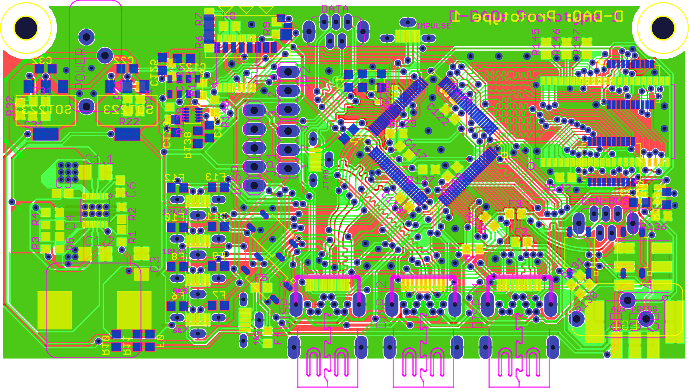
Layout nearly complete...
05/06/2014 at 22:39 • 0 commentsI have to choose some specific terminal blocks for hooking up power, a 5V external sensor via unterminated wires, finish routing power and make sure ground planes make sense. However, except for some minor tweaking in the bottom right and a power reg. for the oscillator (upper middle on bottom layer), board layout seems to be complete. Final board dimensions differ from my latter goal of really close to a credit card, though I'm not far off. A card's area is ~7.17 in^2 and D-DAQ will be weighing in at ~7.25 in^2 with near-final outline dimensions of 3.71" x 1.955".
![]()
Name, version, OHW logo, etc will be on the top right.
-
RTD Measurement Response
05/04/2014 at 20:01 • 2 commentsOne of the trickiest sensors to monitor is an RTD, aka resistive temperature device, imho. They're relatively simple where their resistance changes over a temperature range. These types of sensors are used to monitor coolant/water temps, oil temp, and even air temp. They also have a slow response time, which can easily be 3-5 seconds but usually no quicker than 0.5 s. It's difficult to read them with a regular ADC if their apart of another circuit too. Why? We're loading the circuit and disrupting it's calibration when we tap it. Since its a resistive device, we are basically creating a voltage divider of which their output changes drastically with load. This was one of the first technical hurdles that launched me into developing D-DAQ.
Turns out I needed a high input impedance method to get an accurate reading. This brought me into the world of op amps, and boy, it is a big world... Anyhow, over the course of a year or so, I became more familiar with terms critical to this application such as input bias current and offset voltage. I had watched those videos a few times just to understand what was going on. These 2 specs were very important because the ADC is 10-bit for 3.3 V, which gives ~3.2 mV divisions. Next up, I wanted to minimize error via gain and also use high gain for low readings and less gain for higher ones so I decided to setup a 2 stage amplifier. That, or a logarithmic amplifiers to counter the exponential response of the voltage increase.
How to implement such was tricky and the interwebs provided a few solutions, one of which was a logarithmic amplifier, but few applicable as they would vary over temperature thus causing calibration/characterization problems. I need a precise circuit. How about PWM? Well, even after 2 or 3 RC filters, the output was too difficult to make consistent over various duty cycles. This bumped me over to FETs. I've known about them, but wasn't keen on their operational specifics. A few weeks later after playing around on circuitlab.com, I came up with a response I felt worked really well.
![]()
40 K ohm to 80 ohm. That was is the initial RTD range that I needed to monitor. The circuit the RTD is on is a 5V source with a wire resistance <0.5 ohm. I used a couple regressions to plot extended ranges for the RTD outside the stated spec. As it stands 40K and 20K can give the readout for the same temperature. There will need to be calibration for measuring these sensors on various cars, but from running the regressions, only 2 temperatures are needed. The further apart the better though.
I spent about 9 month on and off trying to figure out a solution. After all, it's basically just math in a physical form. Since it could be done on paper, it could be done physically. Don't give up as there is always a way.
-
Input Captures vs. Analog Inputs with D-DAQ & a DS2072
05/02/2014 at 23:28 • 0 commentsI happen to be lucky enough to own a Rigol DS2072. Thank you to the kinda folks over on the EEVBlog Forums, I decided that this scope would be my first oscilloscope. I've used them in the past but have not owned one. The UI is a bit quirky and not organized well imho, but for what you get in terms of price, it's simply a pleasure to use. Anyhow, back to that in a second...
D-DAQ has 3 interfaces for observing metrics: analog inputs, I2C bus for digital sensors, and 2 input capture pins. The analog inputs are decently spec'd at 10-bit, 1 Msps. Theoretically, I can sample a waveform as quickly as 100 MHz. Why does this matter? There are 2 very particular sensors on my car I want to monitor: Crank Position Sensor and Lift Needle Sensor. First a little background on what they are and why they're needed.
The former is a simple Hal Effect sensor as there is a plate bolted to the crankshaft with 4 gaps in it spaced at 0˚ Top Dead Center, 90˚ TDC, 180˚, and 270˚. Using the output of this sensor the ECU can determine, approximately, where the engine is currently, but also what it's RPM is. I have a 4 cylinder turbo diesel that uses a rotary vane pump and the car is from '97. It's simple, but also quite powerful. In order to properly regulate fuel going into the engine, the ECU needs to know where the crank is so it doesn't inject fuel too early or too late. There is mechanical control, but also electronic adaption as well. The CPS is responsible for reporting back where the crank is.
Now, the lift needle sensor is a bit of an odd ball. It is embedded in the 3rd injector, btw all of the injectors are completely passive and mechanized with 2-stage injection, and consists of a powered coil wrapping around the needle inside the injector. If you'd like to read up more on VE TDIs and their injectors, there is quite a bit of information out there. This particular sensor is responsible to for detecting movement in the lift needle, which indicates when the injector "pops" open and fires fuel into the cylinder. In combination with the CPS, the lift needle sensor is responsible for reporting back when fuel injection occurs, thus what the timing is.
Anyhow, this particular sensor isn't characterized in any documentation online that anyone is aware of aside from one PDF from VW. As a result, a bit of online research pointed to the closest equivalent sensor type, an eddy current sensor. From what I read online, I was expecting that this sensor has a modulated AC signal being sent to it and the ECU had a hardware/software combination for identifying when a peak occurred, i.e. the needle moved. I've been in the TDI community for ~7 yrs, and have been learning about the car(s) for the better part of 3. Everyone I talked to has said that the lift needle sensor is only good for determining when injection starts, thus it cannot be used to determine injection duration.
Why does this all matter? I want D-DAQ to be able to monitor this information and report back timing, SOI (start of injection), and even duration if I can. Here is the technical catch, at 900 RPM the engine is spinning at 15 Hz. Injection occurs in only 2 cylinders during that time, 30 Hz. Though since the lift needle sensor is in only 1 injector and they "alternate" between which cylinder fires (look up 4-stroke engine), I get a pulse once every 7.5Hz. Injection duration is also a very short time, a couple orders of magnitude shorter. When at redline of 5000 RPM, I still only get a pulse from the injector at ~42 Hz. Now, if I were using the analog inputs, I'd have to blindly record values from both the CPS and the lift needle in order to figure out when injection occurs. Doing this for just 1 pulse for detecting what, a +20 KHz signal leads to a lot of trashed data. This is where Input Capture comes into play.
Very simply Input Capture allows to left the bit just sit there until something happens and then it generates an interrupt. This can be from a rising edge, falling edge, or even a pulse. Either way there is a latency of 2-3 clock cycles for the interrupt to be triggered. At D-DAQ's operating freq. of ~65 MHz, this allows me to see ~21,000,000 pulses a second, theoretically. Anyhow, polling for interrupts is horridly wasteful, but if I pass the CPS signal into the the other Input Capture, I can use it as a trigger.
I mentioned earlier that I want to observe fuel injection. As a side note, I know each type of car is different and the ones I have at hand are turbo diesels. D-DAQ is designed to be modular that way if the same type of input is needed, but the characteristics of the sensors differ wildly, only software parameters need to be changed, not hardware. Anyhow, I decided to plug the scope into the car and see if I could characterize the output of the lift needle sensor. I was really curious as to how clean the signal would be and how detailed it was. You may recall that I mentioned that injection is 2-staged. Initially the injector opens with a pilot injection once the fuel pressure is high enough, and then there is the main injection that is then responsible for the remainder of the fuel delivery. Here is what I saw:
![]()
It took me a bit to adjust the scope to be able to pick up the waveform due to how far apart they occur, as I explained earlier. However, when I had this come across my screen, I was ecstatic!!! The first peak is when pilot injection occurred. The second mean, main injection! Finally, the lowest valley you see if when injection ceased, thus end of injection. This is at ~900 RPM at idle on a warm engine.
Delay between pilot and main injection:
![]()
Injection Duration:
![]()
I have a screen capture of the lift needle sensor here at 2000 RPM with cursors turned on, but I did not record the waveform so I cannot pull specifics from it like you see above:
![]()
The last detail that I am leaving with is the that this doesn't appear to be a eddy current sensor. Constant DC voltage is applied to the coil accounting for the 3.7 V offset. Other sensors on this car run from a 5 V supply. I'm assuming that the pilot ignition peak approaches 4.5-5 V when the car is under load. Now, looks like I need to build an amplifier/buffer to remove the offset and scale everything into a 0-3.3V range or some such...
-
Board Layout Timelapse
05/02/2014 at 22:08 • 0 commentsTime for a brake so here are some screens of my board layout progression
February 11th: After placing components down with some trial and error to see how well things fit, I opted to route the most challenging piece at the time: my SRAM frame buffer and octal d-latches. Initially setup to where the longest traces on the top and bottom were roughly the same.
![]()
February 17th: Decided where the mDP receptacles would go and the upright Micro-B USB ports for analog inputs
![]()
February 18th: Though research showed it may not be critical as my highest operating frequency is 80 MHz and 1/20th of the associated wavelength is ~187 mm, best practices says one should have trace lengths match. It's more complicated in the design since I have multiplexed data on the PMP bus to match pin to latch, pin to SRAM data, and latch to SRAM address and assure they're the same lengths, I opted for a cross between all and nothing and matched the lengths of all three trace segments as if they were one. I also determined by rough estimate that I would be able to size D-DAQ to be no larger than 3"x3".
![]()
February 25th: Despite having a huge car battery and alternator for a power source, I wanted to make D-DAQ very energy efficient. Previously I had spent the better part of 2 months combing through numerous datasheets to find the highest efficiency SMPS for the voltage requirements I had: 5V (bott. left), 3.3V (mid. left), and 14V (top left). This was the result of needing such a power plant.
![]()
Work hiatus
April 18th: Fine tune ICSP, place passives and adjust routing, added oscillator, undid I2C work due to oscillator placement
![]()
April 19: MicroSD card layout, more attention to passives, routed the 3 I2C components (temperature & barometer, accelerometer, and digital pot), and began looking at where ground planes needed connecting with vias
![]()
April 21st: ripped up traces to prep for proper component sizing of SMPS parts and went back to my recorded documentation to see how much current per rail I needed.
![]()
April 22nd: Quickly determined that my initial power calculations were being overshot. I don't think it's wise to try and pull 2.3-2.6 Amps from a 2 Amp IC, right? This lead to reshuffling everything based on how much current it needed and which subsystem it got it from. Due to other changed it turned out that I did not need much umph in the 5V rail and the 3.3V rail needed to be beefed up. Looking back and the Doniol gauge, I noted that he used a SOT-223 part labeled L2AA. I quickly found out that LDO regulators had variations where they functioned like boost regulators. Despite my original goal of efficiency, I opted to adjust to having a 12/14.4V to 3.3V SMPS for the main components, have the same input drive the 5V rail via an LDO (ZLDO1117-ADJ) and have the 14V rail driven from the 3.3V rail with the same LDO. Started rearranging the layout for space conservation too.
![]()
April 24th: Rotated the layout 90˚ CW, revised MicroSD card slot to a smaller and more readily available part, added placeholder components for CAN & USB, decided to remove LED indication lighting of the analog inputs.
![]()
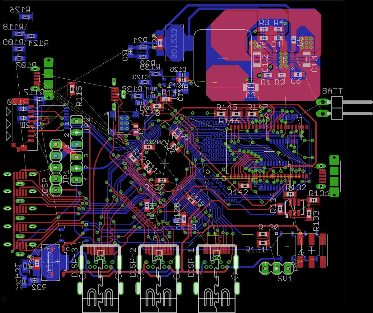
May 2nd #1: Replaced mDP receptacle for one that isn't end-of-life, had to revisit the pinout of the mDP receptacles, removed digital potentiometer and opted for a passive/active combination of accent/backlight control w/ PWM, re-routed analog inputs dropping trace length by up to 33%, re-routed and matched lengths of SPI connections.
![]()
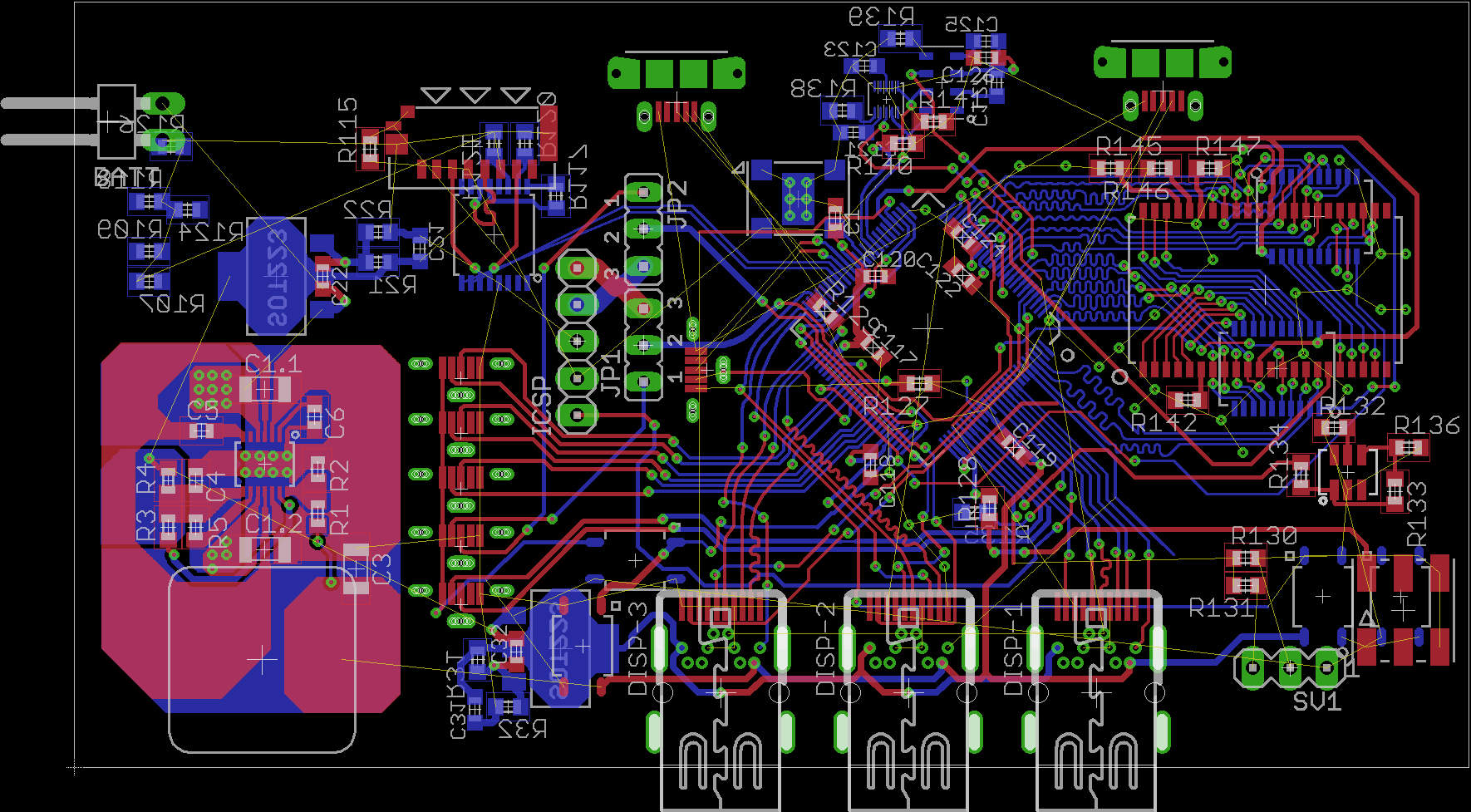
May 2nd #2: Debating the move of the SMPS as noted in my previous log. Haven't finalized it's location, but everything seems to fit better this way and it cleaner as a result (less jumping around with vias). I have room for adding circuit protection on the inputs and power connection.
![]()
-
Layout Crossroads
05/02/2014 at 10:18 • 0 commentsMan, I thought layout wouldn't be changing much after most everything was present... Anyhow, I'm at a crossroads and would appreciate some feedback. The SMPS takes up a hefty sum of board space. Originally I was going to locate it near the frame buffer/SRAM. I'm not worried about EMI as there are ground planes on the top and bottom layers for about 1/4" before nearing any traces of the parallel buss. However, this is an odd spot for the SMPS subsystem because I don't have anything else that takes up the extra space caused by it.
![]()
My solution is to move it to the left and push the contents of the board to the right. Again, I'm not really worried about EMI as the planes closest to the USB ports are ground planes. The top layer closest to the left edge is the switching plane where noise would emanate. The inductor is shielded and the USB cables for the analog input are shielded so...
![]()
I still have cleanup and circuit protection to implement and I have room on either form factor to add the necessary components. The dimensions of both are approximately 3" x 2.6" for the top one and 2" x 3.8". Which would you prefer?