Close
0%
0%

FTDI-be-gone

My version of the ubiquitous USB serial port gizmo

Similar projects worth following
Starting from
$15.00
nsayer has 2363 orders / 163reviews
Ships from United States of America
There are countless devices to add a traditional DB9M serial port via USB. The general problem is that when you just buy a cheap one, you don't have any idea what's inside. With the reminder of the recent FTDI shenanigans, it's become more important to use modem "class" chips that use generic OS drivers rather than proprietary driver devices. Cypress Semi's CY7C65213 is one such device. Because it uses drivers supplied by the OS, there's no opportunity for them to attempt to weaponize a proprietary driver (except for Windows - you still need a driver there).

Note that FTDI is a trademark of Future Technology Devices International Inc. Its appearance here in no way implies an endorsement by FTDI (quite the contrary).

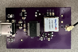
This project, in principle, is quite simple - it's two chips - a Cypress Semi CY7C65213-32LTXI and a Texas Instruments MAX3243ECRHBR. The former is a USB UART. It's pin compatible with the FTDI FT232R's QFN variant, but instead of a proprietary driver, it implements the modem class, so generic drivers provided by the OS will match it. It supports a TX and RX LED, and will be connected up to a micro-USB connector. The other chip is a 3-out/5-in RS-232 level shifter. It requires 4 capacitors to run a charge pump to generate the bipolar supply required for RS-232 signaling, but other than that (and a bypass cap), it requires nothing else.

There are two control inputs on the MAX chip - FORCEON and !FORCEOFF. The chip has some relatively sophisticated activity detection circuitry to automatically shut the chip down when invalid levels are present on the RS-232 side. While that's a nice idea in principle, we don't necessarily want to enforce connecting all of the signal lines up. So FORCEON will be pulled high. !FORCEOFF is intended to be a shutdown signal. The CY7C has a !POWER output pin which is asserted only once the device has been properly enumerated. In keeping with best practices for USB devices, we'll connect !POWER to !FORCEOFF so that the level converter is powered up only when the UART is. The MAX chip has one receive channel that has an alternate output that is always enabled. But since FORCEON is held high, it's moot, so it will be left disconnected.

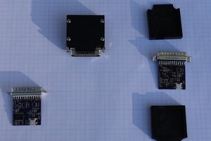
That's all there is to the project electrically, but I wanted to make this into something small that could be used semi-permanently to adapt RS-232 peripherals to USB. So the intent is to design a housing that looks like a molded DB9 shell, but instead of a cable coming out of the back, it simply presents the micro-USB socket.

At the moment, the board is 1.3x0.6 inches, which won't quite fit in cable housings as they're presently designed. The hope is to be able to design a custom enclosure that has the same dimensions on the DB9 end, but tapers down to an acceptable shape ending in the USB port. Additionally, a couple of holes that can be used to install light pipes to bring the RX and TX LED indications to the surface of the case would be nice. I have zero 3D modeling skills, so that's going to be the challenging part of this project.

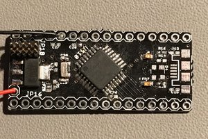
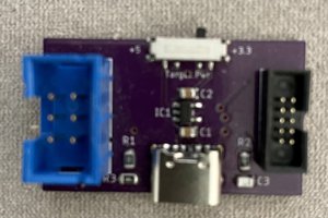
There's a second variant of the board that simply leaves off the RS-232 level conversion chip. That variant has a 6 pin SIP header with the standard Arduino "FTDI" pinout. You can solder a male SIP header onto it and plug it right into a breadboard, or a right-angle female SIP header and plug it into some other device with the mating header. Since this variant passes Vcc out to the target device, a couple of protective measures should be taken to protect the host and insure that the device remains within the USB specifications concerning current draw. A USB device isn't permitted to draw significant current until the host completely enumerates it, which gives the host a chance to figure out that the device would draw more current than is available. The !POWER pin noted above can be used to signal that. In our case, we can tie it to a P channel MOSFET to allow us to turn output power on and off. In addition, we can put in a solder jumper to allow us to output either 3.3 volts or 5 volts (to make 3.3v, we need to add a small LDO). We can tie the selected voltage to the CY7C65213's VCCIO pin so that the signaling is the correct voltage as well. Lastly, we will use an AP2331 current limiting switch on the output to protect the host from inrush.

CypressDriverInstaller_1.exe.zip

Windows driver installer

Zip Archive - 20.65 MB - 12/10/2022 at 04:10

Download

FTDI-B-G-232.pdf

Adobe Portable Document Format - 27.21 kB - 01/02/2022 at 06:58

Preview

FTDI-B-G-232.sch

sch - 164.31 kB - 01/02/2022 at 06:59

Download

FTDI-B-G-232.brd

brd - 51.66 kB - 01/02/2022 at 06:59

Download

USB_TTL.pdf

Adobe Portable Document Format - 30.19 kB - 08/10/2021 at 20:38

Preview

View all 10 files

  • 1 × CY7C65213-32LTXI Microprocessors, Microcontrollers, DSPs / USB Microcontrollers
  • 1 × MAX3243RHB Interface and IO ICs / RS-232, RS-422, RS-423 and RS-485
  • 1 × 10µF 0805 ceramic capacitor
  • 3 × 1µF 0805 ceramic capacitor
  • 4 × 0.33µF 0805 ceramic capacitor

View all 16 components

  • Windows driver

    Nick Sayer12/10/2022 at 04:14 0 comments

    Well, it turns out that Windows still needs a driver. I've put the driver installer package in the files section for those of you who don't run a better operating system.

  • An RS-232 adapter for the TTL variant

    Nick Sayer01/02/2022 at 07:03 0 comments

    I actually made this for the isolated variant, because I didn't want to complete the matrix by making an isolated RS-232 variant. What it is is simply an RS-232 level converter and a DB-9 on a board that plugs into the 10 pin connector for the TTL level variant.

    It doesn't matter whether the power is jumpered for 5 or 3.3 volts. The converter chip works either way.

    It's designed to have a 5x2 .1" DIP header mounted on the bottom side of the board, and plugged into the UART board in such a way that the DB9 is facing the opposite direction of the USB-C connector.

  • USB C

    Nick Sayer07/19/2020 at 15:30 0 comments

    I've updated the design to switch from micro-B connectors to C connectors. In principle, this doesn't really change the design very much at all, except to add the two CCx pull-down resistors. The board has to by physically slightly larger but it's not that big a deal.

    The TTL variant has also changed to supply all 8 signals rather than just 4. There is now a 10 pin DIP header that has the same pinout as a DTE DB-9 RS-232 connector would, with pin 10 being the power supply pin. Although this is not the industry standard pinout (the so-called FTDI 6 pin connector), it's far more versatile, and you can use SIP jumpers to make any pinout you might want anyway.

  • Oops

    Nick Sayer03/21/2016 at 12:59 0 comments

    The latest boards for the RS-232 variant have a little problem.

    I switched from using !SLEEP to using !POWER for the !FORCEOFF pin. Well, !SLEEP and !POWER sort of have opposite meanings. I had intended to use !POWER because it is an indication of the chip either being in USB suspend OR not yet being successfully enumerated. The trouble is, it's low when that happens. !SLEEP was low when in USB suspend. !POWER is high during USB suspend.

    It turns out, though, that I can go back to using !SLEEP for the RS-232 variant, because prior to enumeration, you're allowed to pull up to 100 mA while in suspend you're only allowed 2.5 mA. Using !SLEEP to power off the level converter, therefore, is necessary, but turning off that chip before enumerate isn't.

    I also can salvage the boards I have now by remapping the GPIO pins with Cypress' configuration utility.

    This won't affect the TTL variant boards that are on the way, because the MOSFET that gates power for the output header really does need an active-low power signal. So there's that.

  • New ideas for the TTL variant

    Nick Sayer03/05/2016 at 04:38 4 comments

    I've been thinking some more about the TTL (as opposed to the RS-232) variant. The TTL variant is designed to have the traditional 6 pin SIP header output.

    Many traditional FTDI style interfaces just connect the Vcc output pin directly up to the output, which in principle violates the USB specification, as you're not allowed to draw significant current before the host has properly enumerated the device.

    The fix for this is to switch the Vcc pin on and off with a MOSFET driven by the !POWER pin of the UART. In addition to this, an AP2331 current limiting switch can be used to protect the UART and the host from inrush or other problems. Since the CY7C65213 doesn't run internally at 3.3 volts, if we want to provide 3.3 volt functionality, we'd need to add an LDO. That's actually just as well, since we want to support up to 200 mA of supply current from the Vcc pin. Because of that, we'll specify in the bus enumeration parameters that we require up to 250 mA of bus current. You can do this using Cypress Semi's configuration utility (it's part of their SDK for Windows).

    Anyway, take a look at the schematic in the PDF and let me know what you think.

  • Two more changes for the next rev

    Nick Sayer02/27/2016 at 07:39 0 comments

    The current version works fine electrically, but some of the silkscreen wound up on the wrong layer, so I've fixed that. Another minor issue is that the GPIO I chose to use for the !FORCEOFF line is defined as !SLEEP, but there's another called !POWER that's a slightly better choice. Lastly, the 10 uF cap is just a little too close to the USB connector for comfort, so it has to move just a touch North.

    Other than that, the design is perfect, and the next step is designing the 3D printed enclosure for it. I'm not sure how that's going to happen, as I have zero skills there.

  • Initial boards are on their way

    Nick Sayer02/24/2016 at 17:06 0 comments

    The first boards from OSHPark are on their way. There is on error on the boards, but it's not very important - the "Geppetto Electronics" is on the top silk layer instead of the bottom, so it's interrupted and covered by all the components. The next version will fix that.

    The OSHPark shared project board is here, but because of the QFN chips, you should use a stencil for the pasting. I got one at OSHStencils. You can make one from the paste gerber using the EAGLE files in this project's file section.

    The TTL variant is being processed by OSHPark right now.

View all 7 project logs

  • 1
    Step 1

    Because two of the components are QFN-32 packages, it's important to obtain a paste stencil and use it properly to insure the correct amount of paste is applied exactly in the right spots.

    Note, that it is incorrect to apply paste to the entire exposed pad on the bottom of a QFN package. Too much paste will result in a "bubble" under the chip that will lift it up from the board, making it more difficult for the solder on the pads to reach the pads on the package. Too little paste and the package won't be able to "float" enough during reflow to insure that the surface tension on the pads can properly align the package. In general, the correct amount is somewhere between 40% and 70%, but that will vary depending on how thick the paste stencil is. I strongly recommend either a steel stencil or a 3 mil kapton stencil. Place the QFN devices and the USB connector carefully with a vacuum placing tool. The remaining components are not critical.

    Make sure the paste stencil doesn't have apertures over the DB9 edge-mount connector pads. Those will be hand soldered later.

  • 2
    Step 2

    Take the DB-9 male connector with PC pins and gently pinch the two rows of pins slightly closer together. The row spacing is 2.84mm, but the standard FR4 board thickness is 1.6mm. Your goal is to pinch the pins so that the board is centered between the two rows of pins. Place the board between the pins, so that the pins are neatly centered on the pads. Try and place the board up against the connector as much as possible. Solder pin one on the top side and then check the board's alignment. Look at the board and connector from the side and insure that the board is straight and perpendicular to the connector. Turn the connector over and solder pin 6 (opposite corner from pin 1). Check the board and connector to insure they're straight and square and then solder the remaining pins.

  • 3
    Step 3

    After reflow, check the USB connector pins and the QFN pads to insure there are no bridges. If there are any, clear them with an iron, or if necessary, braid.

View all 5 instructions

Enjoy this project?

Share

Discussions

hrv231 wrote 09/15/2021 at 20:29 point

Hello Nick,

I recently found your project and bought 2 of the ftdi-be-gone, they work perfectly and the lights for rx and tx are really helpful.


I would like to suggest a small change to the design, I would like to see like a clone of the same project but with an RJ45 termination on it, instead of the rs232 plug.

So.. same electronics inside for the rs232 signal but with a rj45 female plug, I bet many people will appreciate the value of having the same electronics but in a smaller package, and your change on the board will be nothing.

Below are some photos with the adapter I use for this.

https://imgur.com/gallery/VTVb8f6


Thanks for your time.

  Are you sure? yes | no

Bree Van Oss wrote 07/01/2021 at 13:38 point

I just received an FTDI-be-gone and so far it works like a charm using OS X. One of the things I'm interested in using it for is to mimic the port names for some of our production devices in /dev. We have logic that will auto detect when certain devices are available by simply looking for a specific device name under /dev. I'm curios if there is a way to use the FTDI-be-gone to accomplish this? Thanks for creating such a cool little project. If this works, we may order a few dozen. 

  Are you sure? yes | no

Mike Turvey wrote 07/21/2020 at 05:34 point

I picked up one of your FTDI-be-gone boards a few years back (v0.3).  It's a really handy little board.  I started a simple enclosure back in 2016, put the project on a shelf, and finally pulled it out again today and wrapped it up.  You can find it here:  https://www.prusaprinters.org/prints/37152-ftdi-be-gone-enclosure-micro-usb

If you'd like me to make a variant for the USB-C version, let me know the exact change in dimensions and I'll make one for that as well.

  Are you sure? yes | no

Nick Sayer wrote 07/21/2020 at 14:16 point

That is super-awesome-deluxe! I've been meaning to do that for a while, but couldn't imagine how to wrap the DB9 shell.

The USB C variant board is 1.325" x .65" (that compares to 1.275" x .6" for the micro-B). The USB C receptacle is a little bit bigger than the micro-B. The web tells me it's just under 9mm wide and 2.7mm tall. It sticks out past the board about .05".

  Are you sure? yes | no

Mike Turvey wrote 07/21/2020 at 19:43 point

Thanks for the dimensions.  I added another set of files to the Prusa site for that version.  If you try it, let me know if it fits or if it needs any adjustments.

  Are you sure? yes | no

Nick Sayer wrote 07/21/2020 at 19:43 point

Thanks! I'll print one when I get home and let you know.

  Are you sure? yes | no

Similar Projects

Does this project spark your interest?

Become a member to follow this project and never miss any updates