Close
0%
0%

NEDONAND homebrew computer

NEDONAND is 8-bit homebrew computer entirely built out of many 74F00 chips (2-input NAND gates)

Similar projects worth following
I started NEDONAND in order to achieve a few goals:
- use only 74F00 chips (2-5 ns delay per gate) to get maximum possible performance (at least 1 million instructions per second);
- 8-bit data, but 4-bit ALU (similar to Z80) with carry/borrow and overflow flags (with approach similar to 6502 where borrow is inverted carry);
- no microcode in ANY form, just 2-stage pipeline and RISC instruction set (similar to PIC - 4 ticks per cycle, 1 cycle per instruction);
- open source (public domain hardware and copylefted software) and hobbyist friendly design (only through-hole components);
- all parts will be well-documented and could be used as standalone addons in other projects;
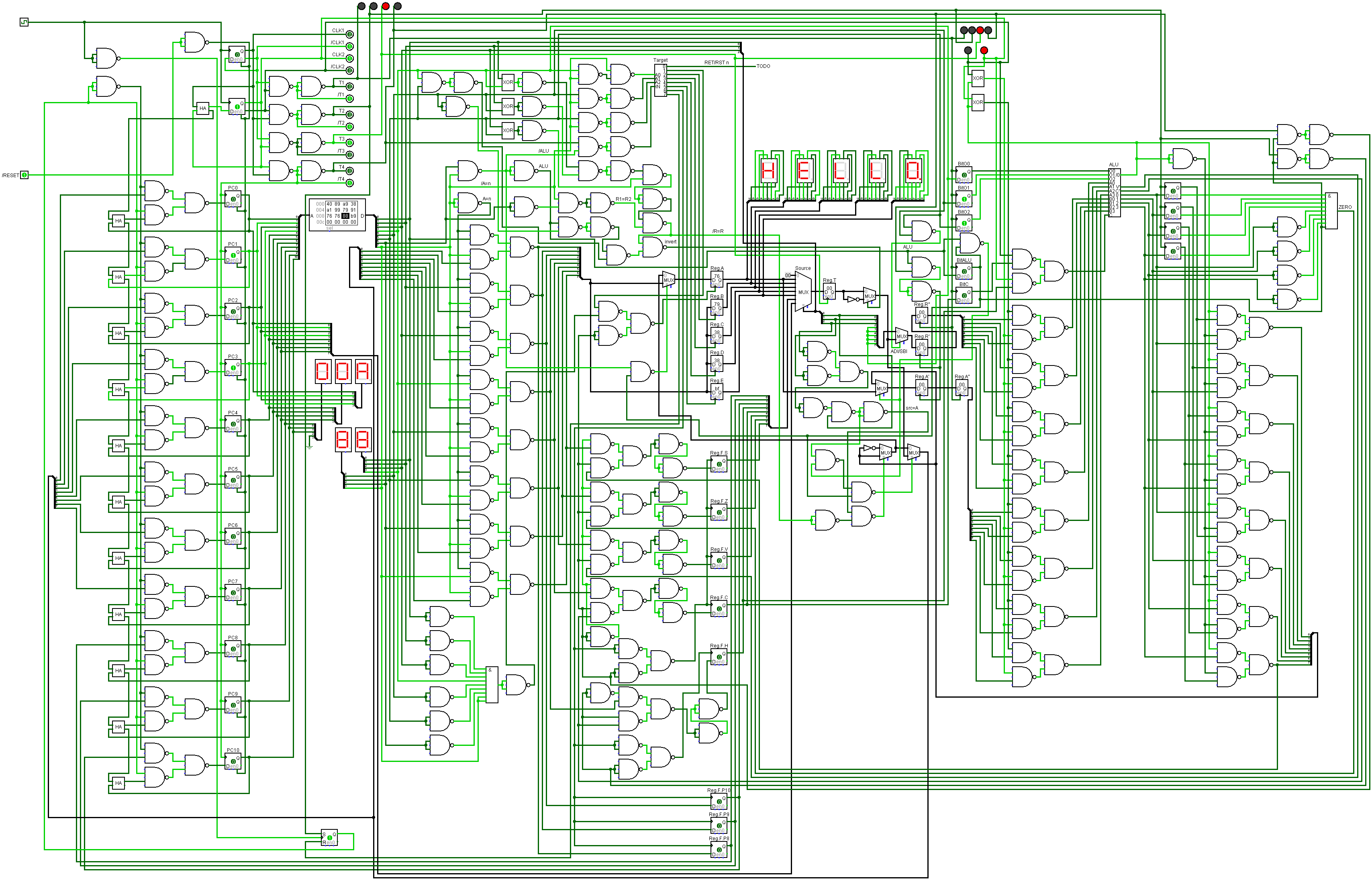
- everything simulated in Logisim first (circuits are provided as a single nedonand.circ file);
- bare printed boards available for ordering through OSHPark;
- plan to build PC-connected "testbed" to test different parts of the project separately;
- and it could be used for educational purposes...

Briefly about architecture and instruction set - it is 8-bit design with 8 registers:

000 - 0 (always zero)
001 - A (accumulator)
010 - B
011 - C
100 - D
101 - E
110 - F (flags and 3 higher bits for jumps)
111 - G (8 lower bits of program counter)

Flags (register F):

bit 7: S - sign (negative result of previous operation);
bit 6: Z - zero (zero result of previous operation);
bit 5: V - overflow (sign overflow in case of add/subtract);
bit 4: C - carry/borrow (borrow is inverted);
bit 3: H - half carry (between nibbles);
bit 2: P10 \
bit 1: P9 - higher bits to set PC in case of jump (reg.G)
bit 0: P8 /

All instructions have 1-byte length:

0xxxxxxx - put 7-bit number into accumulator (A=0xxxxxxx);
10xxxyyy - copy value of register yyy to register xxx (xxx=yyy),
           but if xxx is the same as yyy then invert the value
           and if xxx=0 then it's subroutines RST and RET;
11oooxxx - ALU operation ooo (see below) with register xxx
           (or number), result is stored in accumulator.

ALU operations:

000 - RRC (shift right any register through flag C, res.to A);
001 - RLC (shift left any register through flag C, res.to A);
010 - NAN (bitwise NAND between any register and A, res.to A);
011 - XOR (bitwise XOR between any register and A, res.to A);
100 - ADC (add any register to accumulator with carry C);
101 - SBC (subtract any register from A with borrow /C);
110 - ADI (add 3-bit number to accumulator);
111 - SBI (subtract 3-bit number from accumulator - see below).
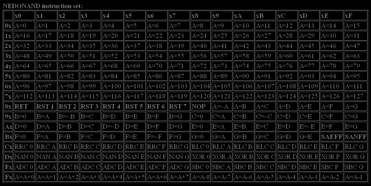
Some comments about opcodes (* if not yet implemented):

OpcodeDescription
00..7FA=n copy instruction to A (n=0..127)
80..87RET (swap + skip) and RST n (prepare F' & G' and swap) *
88NOP (instead of A=0 that could be done differently)
89..BD
R1=R2 if R1 and R2 are the same then store inverted value
BE, BF SAEFF (Skip if A is Equal to 0xFF) and SANFF (Skip if A is Not equal to 0xFF) *
C0..FF
ALU operation (2nd stage of pipeline is used)

Aliases:

CLC is A=A+0 (clear flag C)

SEC is XOR 0 (set flag C)

AFF is NAN 0 (store -1 to A)

Note: F=~F and F=G could be changed to memory access A=[DE] and [DE]=A or something like that...

Resets (similar to Intel 8080):

RST1 - call 0x008
RST2 - call 0x010
RST3 - call 0x018
RST4 - call 0x020
RST5 - call 0x028
RST6 - call 0x030
RST7 - call 0x038

RET (0x80) will return control back from RST subroutine (this part is not yet designed), but if called from higher level will behave as HALT (added on 03/26/2016)


All source codes are freely available and trackable through git: GitLab (since June 2018)

You can purchase proven NEDONAND boards on OSHPark: OSHPark/Shaos

Hardware files for Eagle v5.12 and gEDA (pcb) in ZIP archives: Eagle files, gEDA files

nedonand.circ

Logisim simulation of NEDONAND LITE with library components built from NANDs

circ - 382.35 kB - 03/27/2016 at 01:22

Download

nn1check-200ns.txt

Analyzed invalid outputs (only at 200ns moments for some combinations of input parameters)

plain - 12.52 kB - 03/15/2016 at 23:27

Download

nn1-400ns.txt

Logs from 4-bit ALU testing with samples taken at 400ns, 800ns, 1.2us, 1.6us and 2us.

plain - 80.01 kB - 03/15/2016 at 23:24

Download

nn1-200ns.txt

Logs from 4-bit ALU testing with samples taken at 200ns, 600ns, 1us, 1.4us and 1.8us.

plain - 80.01 kB - 03/15/2016 at 23:23

Download

  • 999 × 74F00 Four 2-input NAND gates with 3.5 ns avg delay
  • 999 × 0.1uF tantalum capacitor One capacitor per chip

  • NEDONAND won 1st round of the Prize!

    SHAOS05/02/2016 at 17:21 3 comments

    NEDONAND became a finalist of the 1st round of Hackaday Prize 2016 along with other 19 great projects!

    Thanks to everyone involved :)

    http://hackaday.com/2016/05/02/these-20-projects-won-1000-in-the-hackaday-prize/

  • Wirewrapping Motherboard

    SHAOS04/17/2016 at 22:10 3 comments

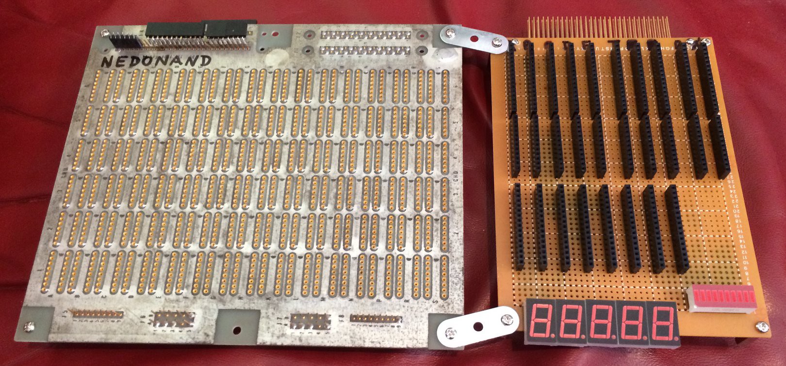
    This is a motherboard to connect all parts of NEDONAND together. I decided to use "wire-wrap" technique, but because female header receptacles are relatively new and not exist in wire-wrapping form (with long terminals with square post) I used "side-kick" soldered board where I collect all header receptacles for NEDONAND boards (probably I will need another one to host everything):

    On the top of a side-kick you can see sockets for registers A,B,C,D,E and T (temporary register) and some other things as multiplexers and demultiplexers. Five 7-segment indicators will show registers contents (directly without decoding) for registers A,B,C,D,E and 10-LED bar graph on the right to show content of register F plus 2 additional signals (as ALU usage flag for example). Golden header on the very top of a side-kick is an interface between wire-wrapped universe and soldered universe to make things easier...

  • Board NEDONAND-16 tested

    SHAOS04/05/2016 at 04:36 2 comments

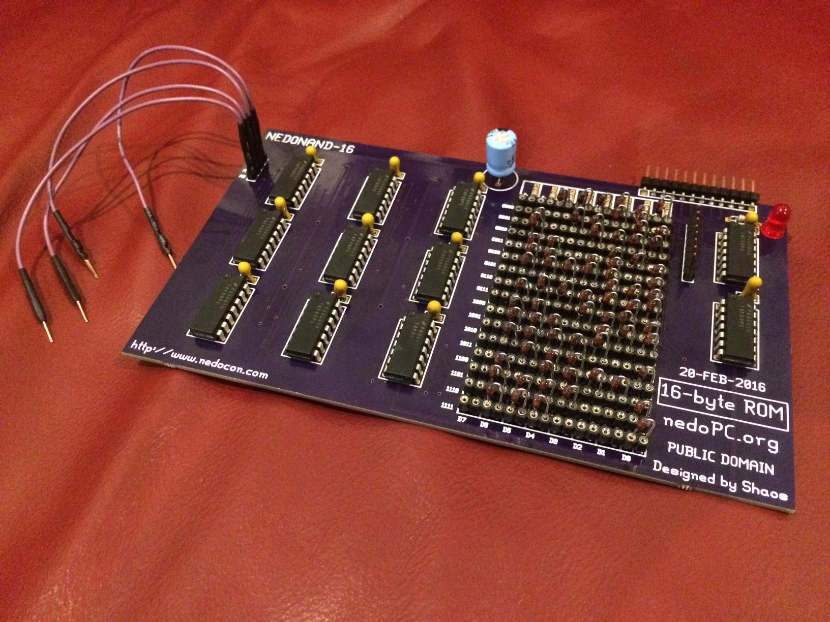
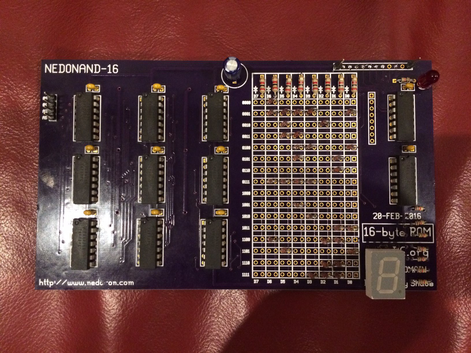
    Finally I completely built and tested NEDONAND-16 board that is MPROM (Manually Programmable Read Only Memory ;)

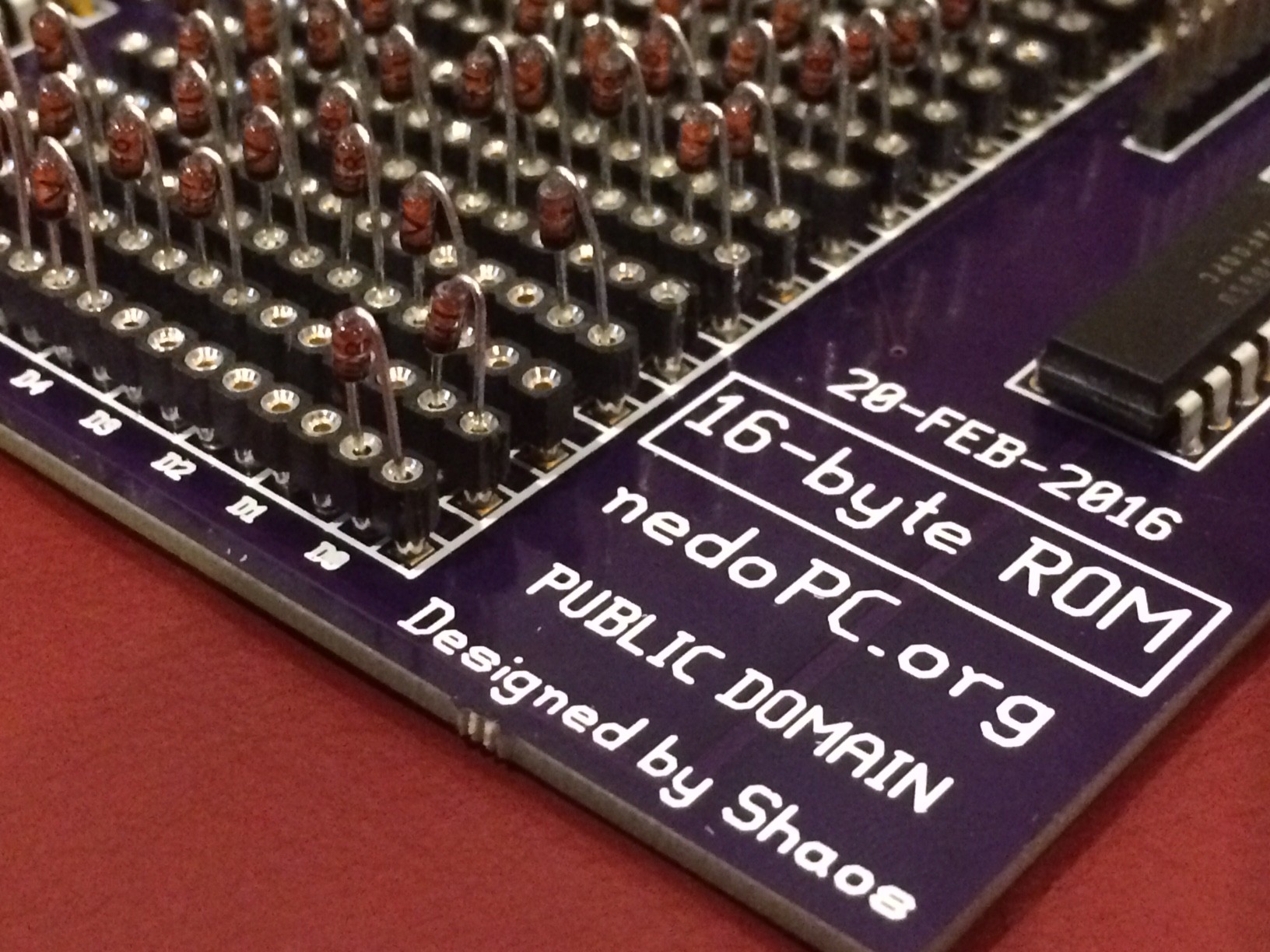
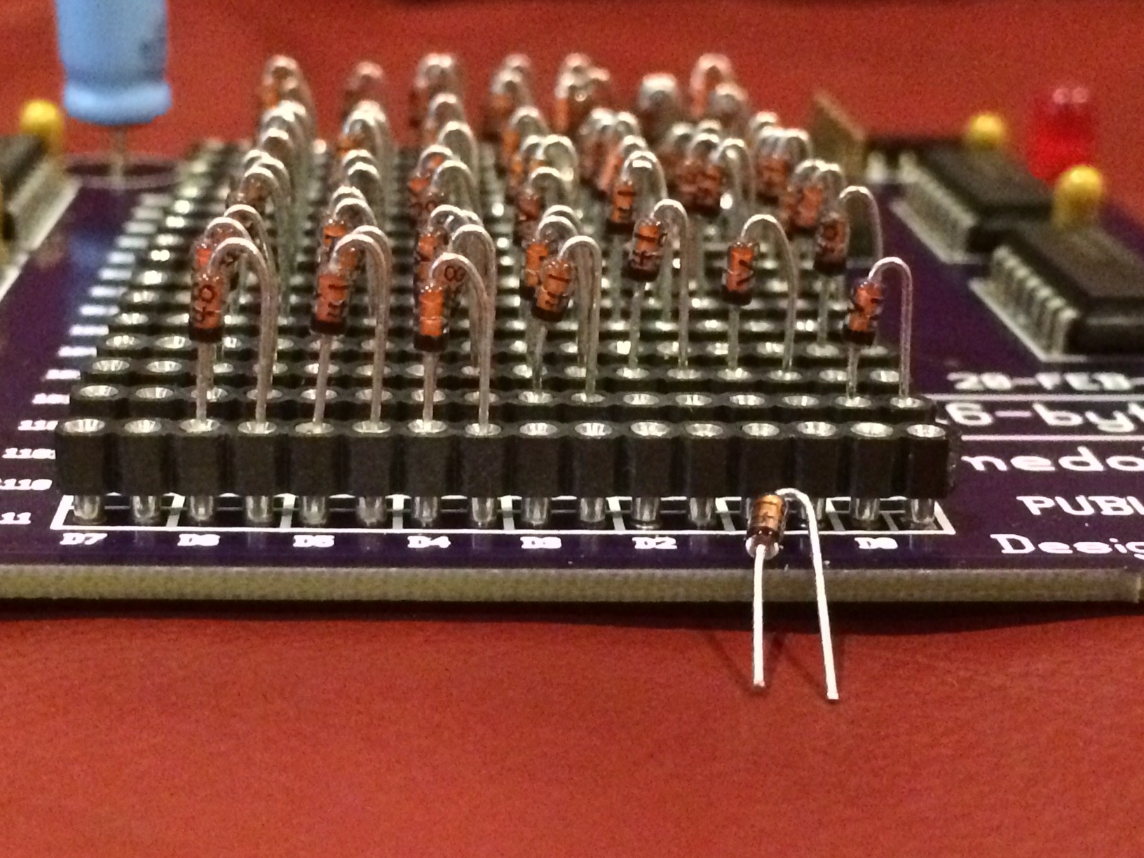
    It's programmable by inserting diodes into holes in proper places:

    In order to do that diode's terminals must be specifically formed:

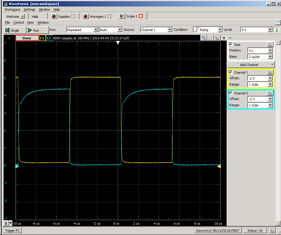
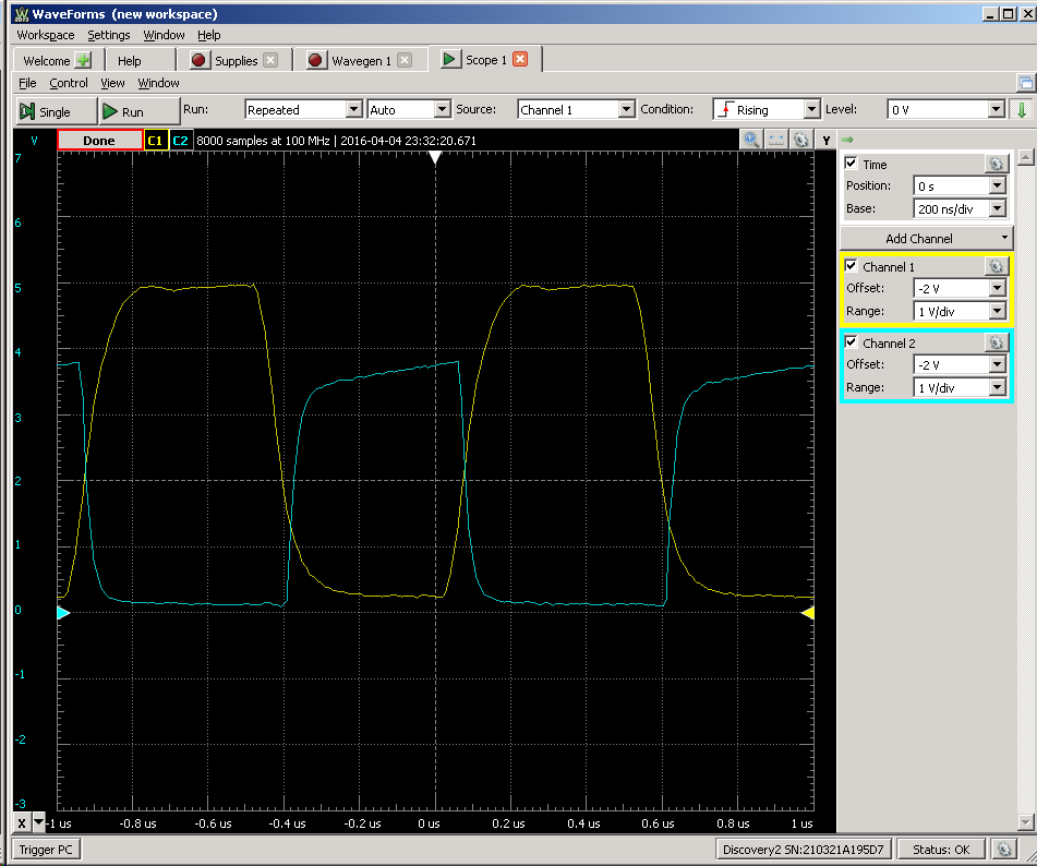
    I connected it to my Analog Discovery 2 and tested its limits in terms of frequency:

    So this is 100 kHz:

    And this is 1 MHz - should be good enough for TTL:

    P.S. But I redo this board anyway, because couple wires still may short on some copies of the board...

  • 7-segment characters

    SHAOS03/27/2016 at 12:24 3 comments

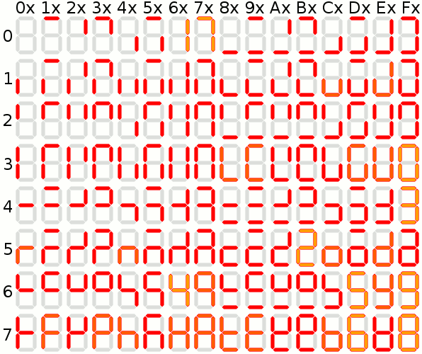
    There is a very useful Wikipedia article about this topic:
    https://en.wikipedia.org/wiki/Seven-segment_display

    Especially the table with 128 7-segment "characters" - I put hexadecimal digits around it to make it easier to see what to send to the register to display (and highlighted everything looks like numbers or letters):

    NEDONAND LITE has this table for "characters" with codes from 0x00 to 0x7F - and next 128 characters with codes from 0x80 to 0xFF simply add a dot at the right-bottom corner. Five indicators display content of 5 registers A, B, C, D and E.

  • NEDONAND LITE with HALT mode

    SHAOS03/27/2016 at 01:35 0 comments

    I added HALT mode into simulation - if any instructions from range 0x80...0x87 is executed (these are placeholders for future RET and RST n) then processor is HALT until user pressed GO button (on the left side of simulation):

    It may help to run large test program when result of every sub-test is displayed on 7-segment indicators with following HALT and when user checked the result he/she may press GO button to run to the next sub-test and so on.

    Logisim simulation file was updated: nedonand.circ

    P.S. This behavior will still be available even in future full-scale NEDONAND when RET instruction is called from the main program (return stack is empty in this case)

  • NEDONAND lite simulation is ready

    SHAOS03/20/2016 at 12:44 0 comments

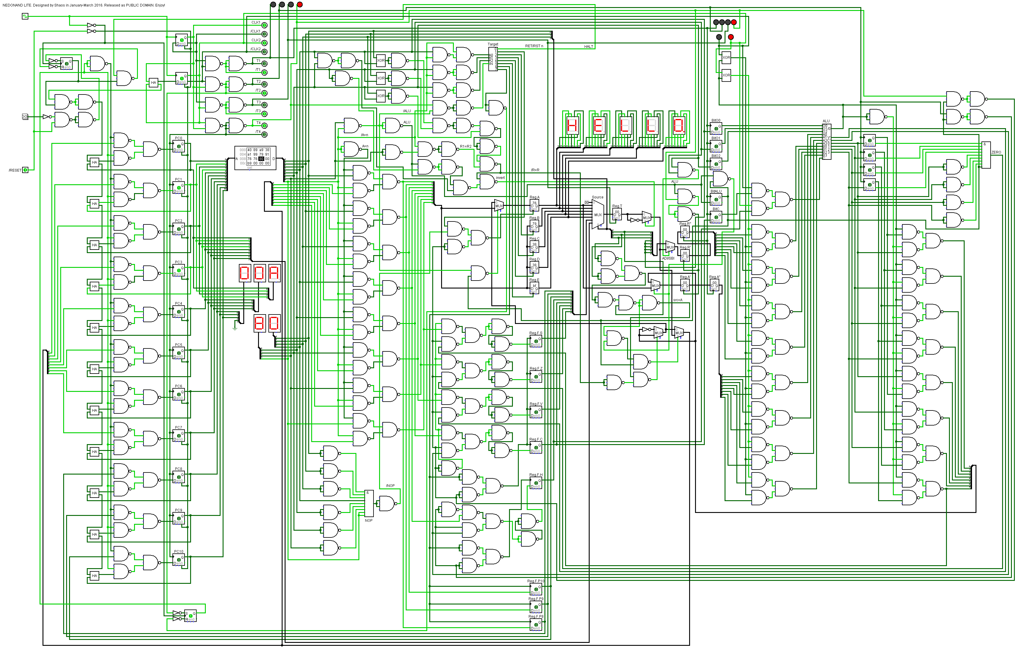
    Simulation of all straightforward commands is ready (everything except RST n, RET, SAEFF and SANFF that require special treatment) with both pipeline stages (2nd stage is having 4-bit ALU that works sequentially in 2 steps to handle 8-bit data). The only special command added is NOP (0x88) and 0xBE,0xBF are still G=F,G=~G. Let's call this subset "NEDONAND lite" - it's pretty much usable even in this state, because bunch of edge-cases mentioned in previous log post was already handled - see Logisim screenshot:

    Interesting thing is that in order to integrate 4-bit ALU (that itself consists of 30 chips 74F00) I added muxing-demuxing logic that consists of about 20 chips 74F00 or 66% of ALU, so it's just a little less than adding 2nd 4-bit ALU in parallel to achieve 8-bit operations. Another observation - having instructions that executed in different stages of instruction pipeline (some in 1st as register copying and some in 2nd as instructions with codes 11xxxxxx that use ALU) is very tricky and require precise edge-case analysis and handling in hardware...

    P.S. Expected waveforms for actual hardware (should be slow enough to work with 2716 ROM):

                _________________
    /RST ______|
         ______   _   _   _   _
    CLK        |_| |_| |_| |_| |_  6.666 MHz
         ______     ___     ___
    CLK1       |___|   |___|   |_  3.333 MHz
         ______         _______
    CLK2       |_______|       |_  1.666 MHz
    
    
    1st stage of pipeline (fetch and decode + simple execute):
         __________             _
    /OE            |___________|   450 ns
               .        ___    .
    REGRD _____________|   |_____  150 ns
               .       .    ___
    REGWR _________________|   |_  150 ns
    
               | 300ns | 300ns |
               ^           ^
               |   450ns   |
               |           \data ready
               |
               \address ready
    
    2nd stage of pipeline (complex execute through ALU):
                _______        .
    HALF1 _____|       |_________  300 ns
               .    ___        .
    ASTO1 _________|   |_________  150 ns
               .        _______
    HALF2 _____________|       |_  300 ns
               .       .    ___
    ASTO2 _________________|   |_  150 ns
    
               | 300ns | 300ns |
    

    P.P.S. If you want to play with it you may download Logisim file from a file storage: nedonand.circ

  • Lets code a little 2

    SHAOS03/19/2016 at 01:42 0 comments

    ow let's code with remembering the fact that we have a pipeline with 2 stages. 3/4 of all instructions (with codes 0xxxxxxx and 10xxxxxx) use only 1st stage, because ALU is doing nothing when they executed - it's A=n, R=~R and R1=R2 including G=R that does jump to new value of program counter (I'm not sure yet about RST/RET and SAEFF/SANFF). Other instructions (with codes 11xxxxxx) use ALU so they took 2 cycles to work and because of that we may have some situations which require special treatment (with special circuitry around). For example, this is subprogram of 16-bit increment:

    0) A=E ; no ALU involved on the next step
    1) A=A+1 ; ALU will be used on the next step
    2) E=A ; copy A to E, but in the same time ALU will change A
    3) A=D ; no ALU involved on the next step
    4) ADC 0 ; ALU will be used on the next step
    5) D=A ; copy A to D, but in the same time ALU will change A
    
    ALU instructions are on 1 and 4 steps. On steps 2 and 5 we have a conflict - A used and modified in the same time. So proposed solution is modify execution of such copy instruction in place - for example here E=A will turn into E=ALU & A=ALU (both registers get ALU output) and D=A will similarly turn into D=ALU & A=ALU. But what if two ALU instructions with A as an argument used one after another:
    0) RRC A ; on the next step A shifted right
    1) RRC A ; on the next step A shifted again (new A stored?)
    2) RRC A ; on the next step A shifted again (new A stored?)
    3) ... ; here new A stored as a result of previous ALU instruction
    Here we have a little conflict, because A will be copied in the same time when it's buffered for ALU - some tricky circuitry should be done in order to fix it. Slightly different situation when we set or clear flag C before ADC and SBC command - everything should work automagically (with flags at least). Another conflicting pair of instructions that will be widely used to calculate AND:
    0) NAN B ; on the next step ALU should calculate ~(A&B)
    1) A=~A ; here A must be inverted and stored from ALU in the same time
    

    In this case we should execute storing to A - not direct, but inverted! Next one - what if A is modified immediately after instruction with ALU? For example:

    0) NAN B
    1) A=B
    Here ALU output must be ignored (only flags will be used). Accumulator will get value from B at the end on step 1 and not ~(A&B). But if it's direct modification of F:
    0) NAN B
    1) F=0
    then most likely we should use flags from ALU, but PC-bits from instruction...

  • ALU tested by PIC

    SHAOS03/15/2016 at 23:28 0 comments

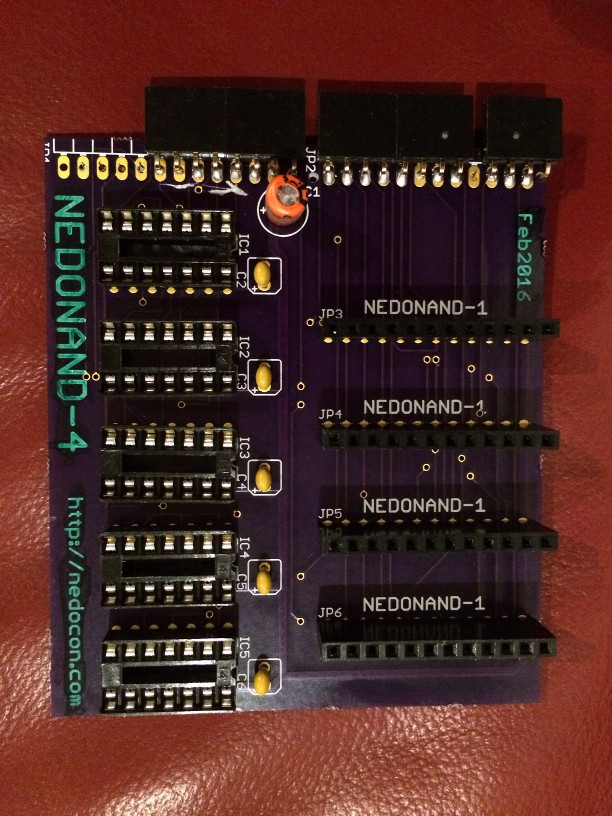
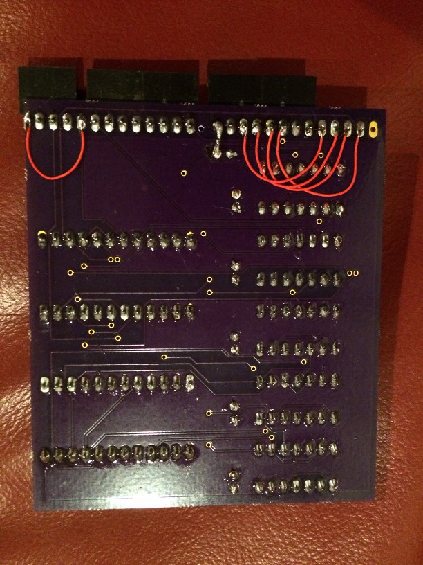
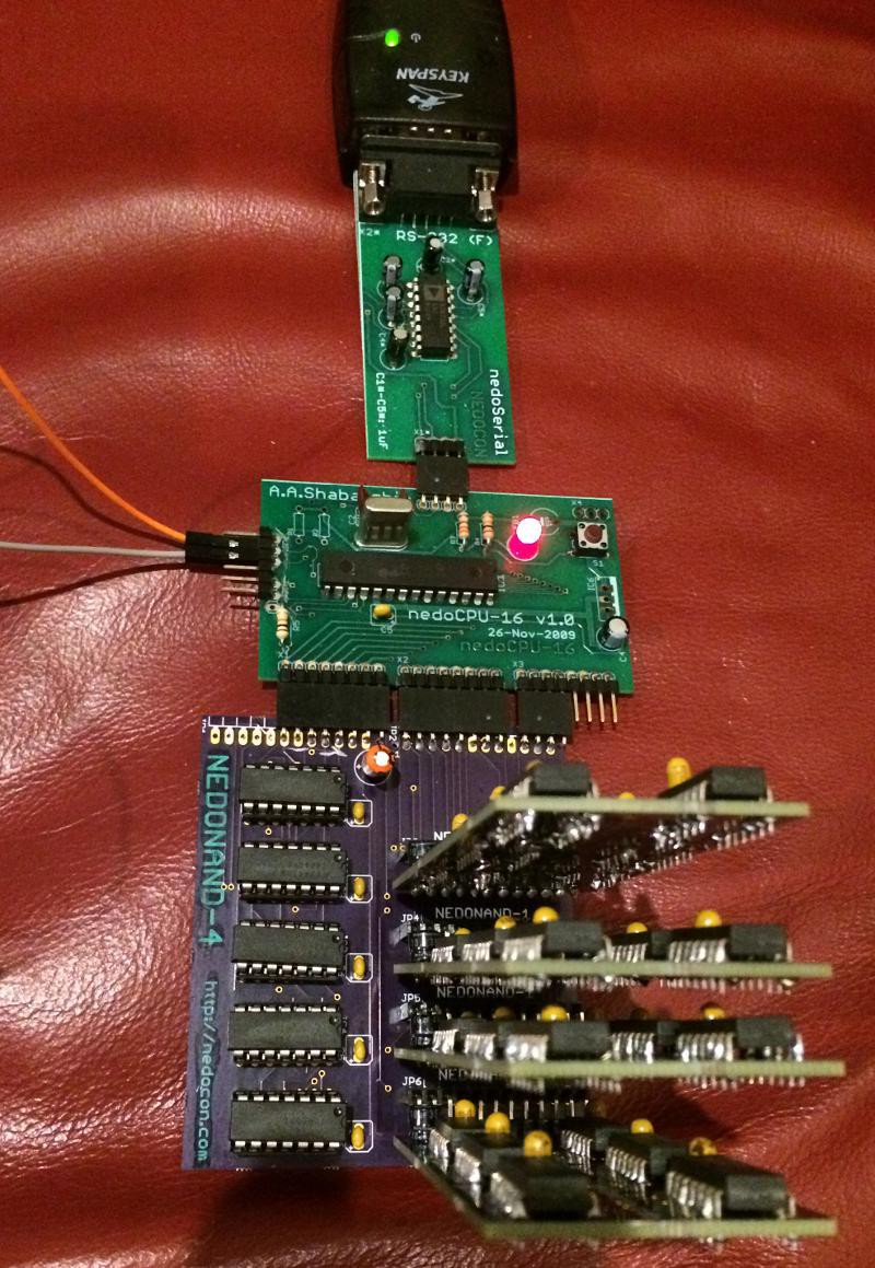
    Today I successfully tested assembled 4-bit ALU (previous revision of NEDONAND-4 board with four NEDONAND-1 connected). In order to do this I slightly modified the board to connect nedoCPU-16 with it:

    Then I wrote a simple program in PIC assembler that worked above PDBL (my Public Domain Boot Loader) to communicate with PC through good old RS-232. Program sent 4096 variants of input vectors (stressing ALU a little before every vector) and sampled output with delays 200ns, 600ns, 1.0us, 1.4us and 1.8us with logging every value:

    Then I wrote C-program that analyze collected logs (see logs) and print report with incorrect values - it's appeared that some ADD operations were not be able to finish in 200ns, but all finished in 600ns (modified program collected 400ns moment also and all finished in 400ns as well - see logs). So ALU worst performance metrics are located somewhere between 200ns and 400ns. This is a little worse than I theoretically calculated using 74F00 spec - I expected 120ns delay (200ns in worst case if all chips have max allowed propagation delay 5ns), but in reality it's somewhere in 200...400ns range. Incorrect samples (here [0] means 200ns after inputs changed):

    ADD 0EC[0] 3F a=-2 b=0 c=1 -> d=-1 (15) c=0 (1) v=0 (1)
    ADD 0ED[0] 3F a=-2 b=0 c=1 -> d=-1 (15) c=0 (1) v=0 (1)
    ADD 0EE[0] 3F a=-2 b=0 c=1 -> d=-1 (15) c=0 (1) v=0 (1)
    ADD 0EF[0] 3F a=-2 b=0 c=1 -> d=-1 (15) c=0 (1) v=0 (1)
    ....
    ADD F8C[0] 03 a=-8 b=-1 c=1 -> d=-8 (0) c=1 (1) v=0 (1)
    ADD F8D[0] 03 a=-8 b=-1 c=1 -> d=-8 (0) c=1 (1) v=0 (1)
    ADD F8E[0] 03 a=-8 b=-1 c=1 -> d=-8 (0) c=1 (1) v=0 (1)
    ADD F8F[0] 23 a=-8 b=-1 c=1 -> d=-8 (8) c=1 (1) v=0 (1)
    

    See full output here. So most of the time it's incorrect most significant bit and/or flags C/V (carry and overflow). And as I said at 400ns everything is correct. Inputs are in formats BBBBAAAACOOO (12-bits represented by 3-digit hexadecimal number before [0]). Outputs are in format DDDVC (5-bits represented by 2-digit hexadecimal number after [0]). Then numbers in parentheses show actual numbers from the board...

    P.S. All source codes are available on GitLab (since June 2018):

    https://gitlab.com/nedopc/nedonand/tree/master/tester/preliminary

  • All boards received

    SHAOS03/12/2016 at 03:52 0 comments

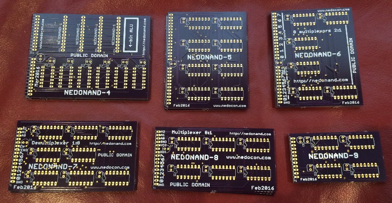
    The rest of the boards just came:

    I think I will connect them together through wire-wrapped "motherboard" (lets call it "NEDONAND-10" ; )

    All of these NEDONAND components could be tested one by one using PIC microcontroller (connected to PC through RS-232) and one 30-pin socket:

        NN1  NN2  NN3    NN4   NN5  NN6  NN7  NN8  NN9  NN16
    --------------------------------------------------------
     1) GND  GND  ---    GND   GND  GND  GND  GND  GND  GND
     2) O0   D1   ~Q0    D0    D0   O0   O0   I0   A    D0
     3) O1   ^C1  ~Q1    D1    D1   O1   O1   I1   B    D1
     4) O2   /R1  ~Q2    D2    D2   O2   O2   I2   C    D2
     5) A    Q1   ~Q3    D3    D3   O3   O3   I3   D    D3
     6) B    /Q1  IN     COUT  D4   O4   O4   I4   E    D4
     7) C    D2   ACT0   VOUT  D5   O5   O5   I5   F    D5
     8) H    ^C2  ACT1   /O0   D6   O6   O6   I6   G    D6
     9) L    /R2  /RESET /O1   D7   O7   O7   I7   H    D7
    10) COUT Q2   CLK    /O2   STB  SEL  /ENO OUT  I    NC (/OE)
    11) DOUT /Q2  NC     /ZERO NC   /SEL EN   NC   AND  NC (/CS)
    12) VCC  VCC  VCC    VCC   VCC  VCC  VCC  VCC  VCC  VCC
    13) ---  ---  GND    ---   ---  ---  GND  GND  ---  ---
    14)                                  A0   A0        ~A0
    15)           D0     O0    Q0   A0   A1   A1        ~A1
    16)           D1     O1    /Q0  B0   A2   A2        ~A2
    17)           D2     O2    Q1   A1                  ~A3
    18)           D3     C     /Q1  B1
    19)           D4     A0    Q2   A2
    20)           D5     A1    /Q2  B2
    21)           D6     A2    Q3   A3
    22)           D7     A3    /Q3  B3
    23)           D8     B0    Q4   A4
    24)           D9     B1    /Q4  B4
    25)           D10    B2    Q5   A5
    26)           D11    B3    /Q5  B5
    27)                        Q6   A6
    28)                        /Q6  B6
    29)                        Q7   A7
    30)                        /Q7  B7
    

  • Another test

    SHAOS03/10/2016 at 05:57 2 comments

    Just put together NEDONAND-3 with 2 NEDONAND-2 and NEDONAND-16 ROM "programmed" with 4-bit to Hex converter to display 4-bit address in human readable format:

    This is ROM alone (I drilled a few holes and installed 7-segment indicator directly on the board):

View all 25 project logs

Enjoy this project?

Share

Discussions

Сергей wrote 05/24/2023 at 07:18 point

Страничка в ВК  https://vk.com/pluton_tut

  Are you sure? yes | no

Сергей wrote 05/24/2023 at 07:17 point

Привет, Занимаетесь еще проектом https://habr.com/ru/articles/496366/   ?

Не могу связаться с автором, не поможеете?

  Are you sure? yes | no

SHAOS wrote 06/07/2018 at 02:56 point

Moved source files of NEDONAND to GitLab:
https://gitlab.com/nedopc/nedonand

  Are you sure? yes | no

Dr. Cockroach wrote 10/30/2017 at 08:55 point

Just wondering how large this could be using my IO style of NAND construction. Speed would be a slight bit slower...

  Are you sure? yes | no

SHAOS wrote 10/31/2017 at 00:13 point

Huge :)
And very hungry for electrical power I think ;)

  Are you sure? yes | no

Squonk42 wrote 05/03/2016 at 06:28 point

I really appreciate your perseverance and I fully understand your motivation of avoiding any microcode, as well as the opportunity to get 74F00 chips at low price.

I don't want to destroy your enthusiasm, but do you know about logic gate combination using multiplexers? Basically, you can implement all Boolean combination of n+1 bits with an n:1 multiplexer:

https://en.wikipedia.org/wiki/Multiplexer#Multiplexers_as_PLDs

As Dieter from 6502.org states: "Multiplexer: the tactical Nuke of Logic Design":

http://6502.org/users/dieter/a1/a1_4.htm

You can configure them as LUT with an overall smaller propagation delay (especially if you use the inverted output, you avoid one inverter...). For a 74F151, it is between 2.5 and 14 ns max, replacing several NAND stages...

And it is great to use them as ROM instead of DTL logic which is very slow. You can build a hand-programmable 64 bit ROM with only 8 chips.

I can share logisim schematics if you are interested.

And keep your motivation intact!

  Are you sure? yes | no

Yann Guidon / YGDES wrote 05/03/2016 at 07:21 point

MUXes are awesome, I use some in #DYPLED but there are different reasons to use the '00...

  Are you sure? yes | no

SHAOS wrote 05/03/2016 at 13:49 point

Yes, I know - I have secret design of a ternary processor that could be built from ternary multiplexers only :)
For NEDONAND I use 74F00s as a given and I also use multiplexers as well, but they built from NAND gates ;)

  Are you sure? yes | no

Squonk42 wrote 05/03/2016 at 14:32 point

OK, then.

But using diodes for MPROM is 1 or 2 order of magnitude slower than using FTTL MUXes as ROM LUT, this is why you are limited to 1 MHz.

  Are you sure? yes | no

SHAOS wrote 05/03/2016 at 14:35 point

1 MHz is good enough for now :)

In future I may create faster version, but it will use actual ROM chip

P.S. Let me explain - for now biggest bottleneck in performance is PC counter because of carry propagation delay - it may take up to 600ns to change address (in case of full 11-bit implementation) - so it's already having 1.666 MHz limit...

  Are you sure? yes | no

Squonk42 wrote 05/03/2016 at 19:54 point

Assuming a 12 bit PC, you can build a 2-bit carry look-ahead using a single 74F151 MUX propagation delay (http://6502.org/users/dieter/a1/a1_7.htm, bottom of page). We are down to 6*(3.5~9)=21 to 54 ns, i.e. from 18 up to 48 MHz... Now you can see why I say DTL PROM is slow ;-) Using MUX ROM, theoretical limit is > 100 MHz.

  Are you sure? yes | no

SHAOS wrote 05/03/2016 at 20:06 point

For program counter I can use 4-bit 74F163 chips that can run with frequencies up to 100 MHz, but it's against the rules :)

  Are you sure? yes | no

Squonk42 wrote 05/04/2016 at 06:00 point

No, you won't reach that speed, unless you use Schotky diodes. Even there, all these parallel wires will add significant parasitic inductance and capacitance that will limit your speed to < 20 MHz

  Are you sure? yes | no

SHAOS wrote 05/04/2016 at 13:18 point

And it's still Ok, I believe :)

  Are you sure? yes | no

Ken KD5ZXG wrote 07/04/2020 at 22:28 point

SHAOS> for now biggest bottleneck in performance is PC counter because of carry propagation delay

Ken> The are two ways to avoid carry propagation delay. For counting, a linear feedback shift register LFSR (pseudorandom generator) can cycle through all numbers save one.  No carry is used and there is no delay for ripple. Maybe this works best for microcode where you can hide the strangeness. You can pull this off with just 74F00, thus worth considering.

Ken> Second and more practical way is a pass through carry. Using real switches like 74CBT series 6nS 5ohm, not combinatorial logic like 74F151. Wire your multiplexors for XOR (A,B) drives MUX(A,CARRY). Carry flows through all switches (or gets replaced by A) at wire speed. Instant carry drives another bank of XOR for the final result. Yes, its a ripple carry adder. Its also a carry skip adder. It doesn't work like either, except it works like both. Its an old relay trick, blame Konrad Zuse.

  Are you sure? yes | no

Kn/vD wrote 04/03/2016 at 14:33 point

That is a hell of a project :-)

Wondering have you calculated the minimum required number of NANDs to build a fully functional system?

  Are you sure? yes | no

SHAOS wrote 04/03/2016 at 15:12 point

NEDONAND LITE (no subroutines, no memory access and no skip-if instructions) requires about 1540 NAND-gates (it's 385 chips 74F00)

  Are you sure? yes | no

SHAOS wrote 03/06/2016 at 14:54 point

Just created GitHub for the project: https://github.com/shaos/nedonand

  Are you sure? yes | no

J. M. Hopkins wrote 02/27/2016 at 12:27 point

First off, I like the project. I had started construction of an 8-bit cpu with 16-bit address space, but lost steam, so I appreciate the effort here.

I'm curious why you didn't use SMD NAND ICs to limit the footprint, I wouldn't think the routing would be too difficult...

Any who, keep it up

  Are you sure? yes | no

SHAOS wrote 02/27/2016 at 18:01 point

I believe that DIP is more "hobbyist-friendly" than SOIC and I believe that "through-hole" assembly is more reliable and can live longer. May be I'm wrong ;)

Also I got bunch of 74F00s as "clearance" a few years ago for 2.9 cents per chip :)

And last argument - I plan to do final glue logic connecting all boards together as "wire-wrap" and it's obviously not applicable to SMD...

P.S. Actually if final assembled circuit will work as expected then I'll probably "autogenerate" SOIC-version of it on a huge single board...

  Are you sure? yes | no

J. M. Hopkins wrote 02/27/2016 at 20:25 point

Gotcha. 2.9 cents each is a great price :) Thanks for the reply

  Are you sure? yes | no

SHAOS wrote 02/27/2016 at 21:00 point

Problem is I use tantalum capacitors 0.1uF which are 20 cents each :)

  Are you sure? yes | no

J. M. Hopkins wrote 02/28/2016 at 00:04 point

I can't even remember how much I purchased my .1uF caps for, had them for do so long in such huge quantities :)

  Are you sure? yes | no

Pete wrote 02/25/2016 at 23:09 point

re: 2, I see.  Say for instance, to perform a JL (jump if less than) where you're checking flags for S<>V, I'm thinking something like this (not sure if the formatting will survive pasting):


SEC                 #always need to set carry before subtraction
A=A SBC B     #example test who's flags we want to evaluate
C=F                 #save the flags to register C for later use
A=01111111         #inverse of S flag bit
A=~A               #A=10000000, bit for S flag
A=A NAND C  #mask out S flag, all other bits 1, MSB 0 if S==1, else 1
A=~A               #A=10000000 (128) if S==1, else 0
A=A RRC 0     #assumes above NAND or NOT cleared carry flag
A=A RRC 0     #now A=00100000 (32) if S==1, else 0
A=A XOR C    #A=C except 32bit flipped if S==1 (1 XOR V => ~V)
                       #IOW, 32bit will be 0 only if S==V
C=A                #save modified flags
                       #for JGE, we could manually flip 32bit again, eg.
                       #A=32, A=A XOR C, C=A
A=00100000 #prepare to mask out 32bit
A=A NAND C #A=11011111 if S<>V, else all 1s
A=~A              #A=00100000 if S<>V, else 0
A=A RRC 0    #assumes above NAND or NOT cleared carry flag
A=A RRC 0
A=A RRC 0    #A=4 if S<>V, else 0
A=A+2           #A=6 if S<>V, else 2
:mark1
A=A ADC G   #assumes carry flag still cleared
G=A               #jump to +0 or +4


# @mark1 + 2: S==V, condition not met
A=6               #offset from mark2 to exit condition
CLC              #needs adjustment for number of conditional statements
:mark2
A = A ADC G
G=A             #jump to exit condition


:condition_true
# @mark1 + 6: S<>V (and Z==1), condition met
NOP            #perform your conditional statement(s) here
NOP            #if it takes 4 or less, you can use JGE instead of JL
NOP            #(flip 32bit again) and skip above jump to exit
NOP


# @mark2 + 6: forward from z==0
NOP            #conditional statement complete, continue


So it takes 18 operands to perform the equivalent of a single JL conditional jump that compares two flags.  It's definitely a trade off of RISC code bloat vs. CISC hardware complexity; are you sure it's worth it?  It's fun (for some) figuring out working assembly code, but, holy cow!!!

How about F8..FC are LDf operands where f is [S,Z,V,C,H] and the operand puts the value 0000000f in A where f is value of the given flag?  Other than FF (aka DEC or A=A-1), I don't see the subtract immediates being used too much.

That would simplify the code above to:

SEC             #always set carry before subtraction
A=A SBC B #example test who's flags we want to evaluate
LDS             #load sign flag
C=A             #save to C reg
LDV             #load overflow flag
A=A XOR C #A=1 if S<>V, else 0
CLC
A=A RLC 0
A=A RLC 0
A=A+2         #A=6 if S<>V, else 2
:mark1
...


Hrmm...  That doesn't save as much as I thought it would.  A simpler comparison, such as JE (jump if equal), does get even easier, though:


SEC             #always set carry before subtraction
A=A SBC B #example test who's flags we want to evaluate
LDZ             #load zero flag
CLC
A=A RLC 0
A=A RLC 0
A=A+2         #A=6 if Z==1, else 2
:mark1
...

Bah!  There goes my whole afternoon.  Thanks for that!!!  :-/

No, really, thanks!  I forgot how much I enjoyed low-level languages.  :-)

  Are you sure? yes | no

SHAOS wrote 02/26/2016 at 00:51 point

Wow, so much coding already ;)

I thought that G=F may help in extreme cases (but whole page must be used then)

OK, I see now that we need something like SKIP-IF-ZERO

So I may propose to move RET (it was G=~G) into place of RST 0 and use G=~G as something like SKIP-IF-A-EQ-FF (SFF?) so jump if equal will look like

E=addr_neq

A=0x40 ; mask for flag Z

NAN F ; A=~(A&F)

SFF ; new magic command (if A=0xFF at this point then tested flag was 0)

G=E ; skip if equal (so jump if NOT equal)

; stay here if equal

A=addr_eq

G=A ; jump to addr_eq

addr_neq:


P.S. Actually G=F  is also not so useful, so we may have both SKIP-IF-A-EQ-FF and SKIP-IF-A-NEQ-FF commands (SAEFF and SANFF?)

P.P.S. Also I'm thinking about moving NOP to 0x88 (second A=0)

  Are you sure? yes | no

Pete wrote 02/26/2016 at 03:21 point

ah.. I like that.

P.S. You might also repurpose F=G and F=~F too.  I would say they're less useful than G=F..

P.P.S. Good. I meant to ask about that but figured you might be stuck on 00 as NOP for some other reason. 

Oh, and I also wanted to ask, SEC as XOR 0: do all XORs set carry or just that one? 

  Are you sure? yes | no

SHAOS wrote 02/26/2016 at 03:35 point

I made all logic operations set flag C and clear flag V (actually only adding/subtraction may set V and all other ALU operations will clear V)

About F=G and F=~F - probably I will change them to something useful as RAM read/write (external 16-bit address bus driven by register pair DE - so in assembler it may look like A=[DE] and [DE]=A), but a little later...

  Are you sure? yes | no

PinheadBE wrote 02/25/2016 at 08:25 point

Now... THAT is something!  I've always wanted to go to my favorite distributor and buy a chip per thousand.   I've finally found a reason!

Really, amazing work, Alexander!  Big thumbs up!

  Are you sure? yes | no

SHAOS wrote 02/25/2016 at 17:32 point

Thanks ;)

  Are you sure? yes | no

SHAOS wrote 02/25/2016 at 04:04 point

Thanks for your interest!
1) G is physically 8 lowest bits of PC, but 3 bits from F are NOT highest bits of PC! Those bits physically located in register F and used ONLY when something is copied to G, so any G=R (where R is any register) will do copying not 8, but 11 bits - 8 bits from register R (actually from intermediate register T where R value was copied a little earlier) and 3 lower bits from register F (it's more or less like PICs handle long jumps). You can check Logisim simulation (nedonand.circ) where this logic was already implemented.

2) Yes, because of simplicity I got rid of all conditional jumps and it became a little tricky to do this using masking F, shifting and adding to G through A...

  Are you sure? yes | no

James Newton wrote 02/25/2016 at 07:20 point

Ah... nevermind my question on your project log, this answered it.

  Are you sure? yes | no

Yann Guidon / YGDES wrote 02/25/2016 at 13:05 point

Ah yes, I recognized the Microchip PIC trick for long jumps, only even dirtier ;-)

  Are you sure? yes | no

Pete wrote 02/25/2016 at 01:22 point

Cool project!  I may just have to fiddle with one of these myself.  I've always liked to study the orthogonality of common ISAs, so it's interesting to see how you've laid out all the instructions.  Thanks for posting this along with the OSHpark link for the boards.


Question 1: In the "Lets code a little" project log, you have:
   5. jump to the beginning of arbitrary 256-byte page (3 bytes):
      00000xxx (A=00000xxx)
      10110001 (F=A)
      10111000 (G=0)
Once you set F (F=A) in the second step, have you not just jumped to the new page at whatever offset G is at when you load the next instruction?  Or is there some gate by which setting F does not change the execution page until an instruction writes a new value in G (but not when it increments by one due to the clock)?


Question 2: What is your plan for conditional branching?
The only way I can see to control flow without conditional branches would be to get the results into G directly.  Eg. rotate or add the carry bit into A, turn it into an offset, add G and move the results into G.  Or for jumps based on multiple flags, you'd have to perform your op, save F, extract the bits you need to test, turn them into offsets into a jump table, and copy the jump offset right into G.  A series of conditional jumps based on flag status (including an easy way to S XOR V) would make program logic MUCH simpler...

  Are you sure? yes | no

Similar Projects

Does this project spark your interest?

Become a member to follow this project and never miss any updates