SHAOS
SHAOS-
NEDONAND won 1st round of the Prize!
05/02/2016 at 17:21 • 3 commentsNEDONAND became a finalist of the 1st round of Hackaday Prize 2016 along with other 19 great projects!
![]()
Thanks to everyone involved :)
http://hackaday.com/2016/05/02/these-20-projects-won-1000-in-the-hackaday-prize/
-
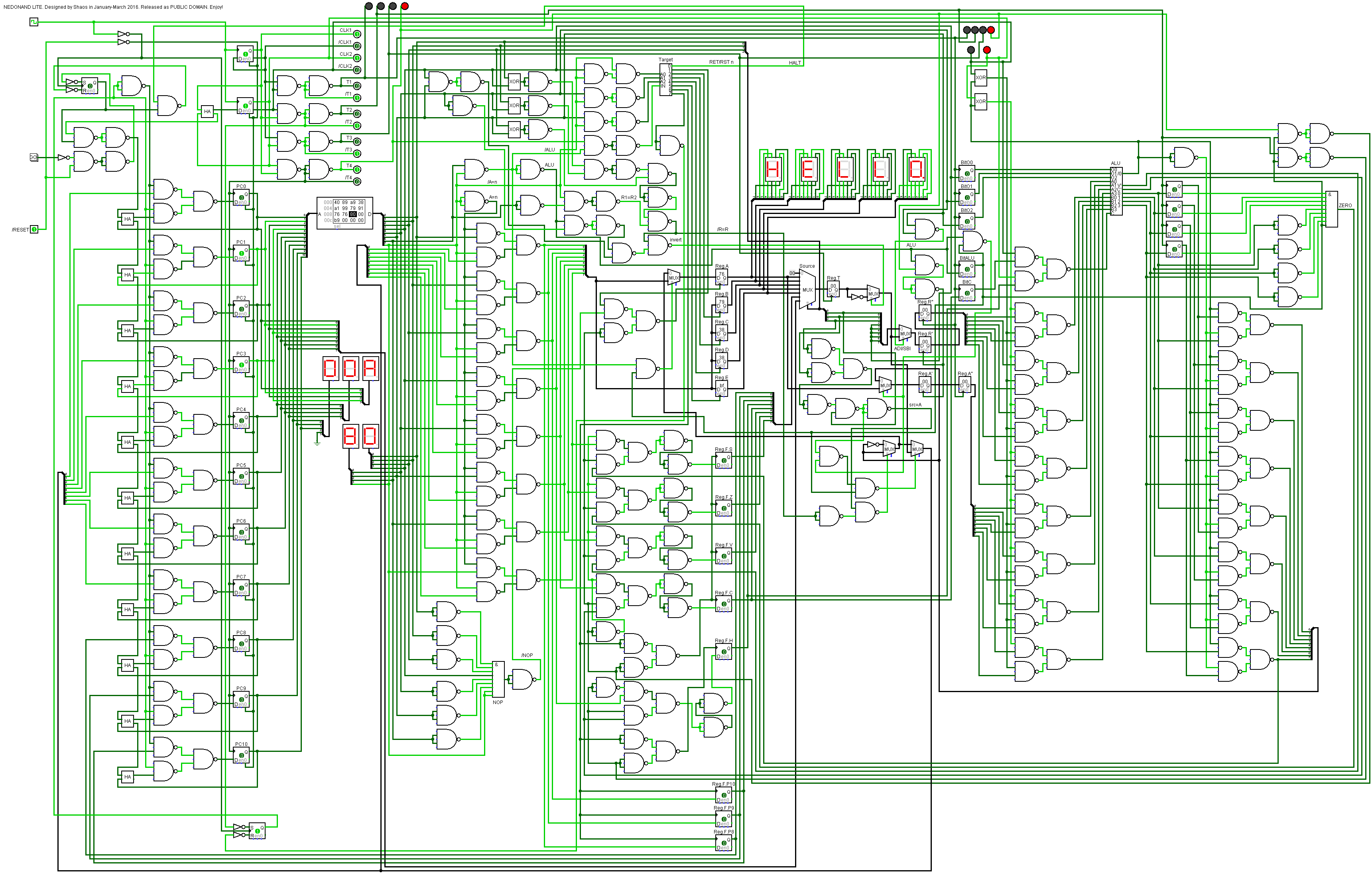
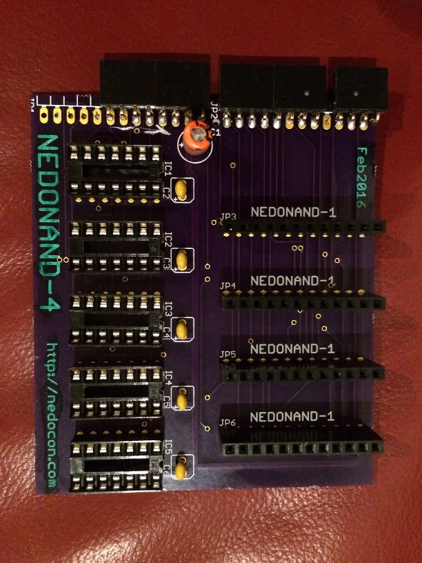
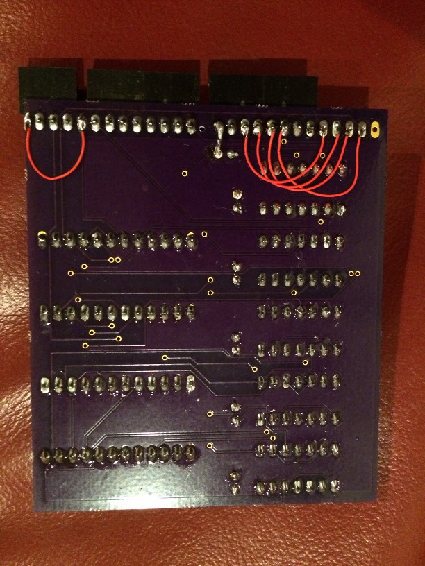
Wirewrapping Motherboard
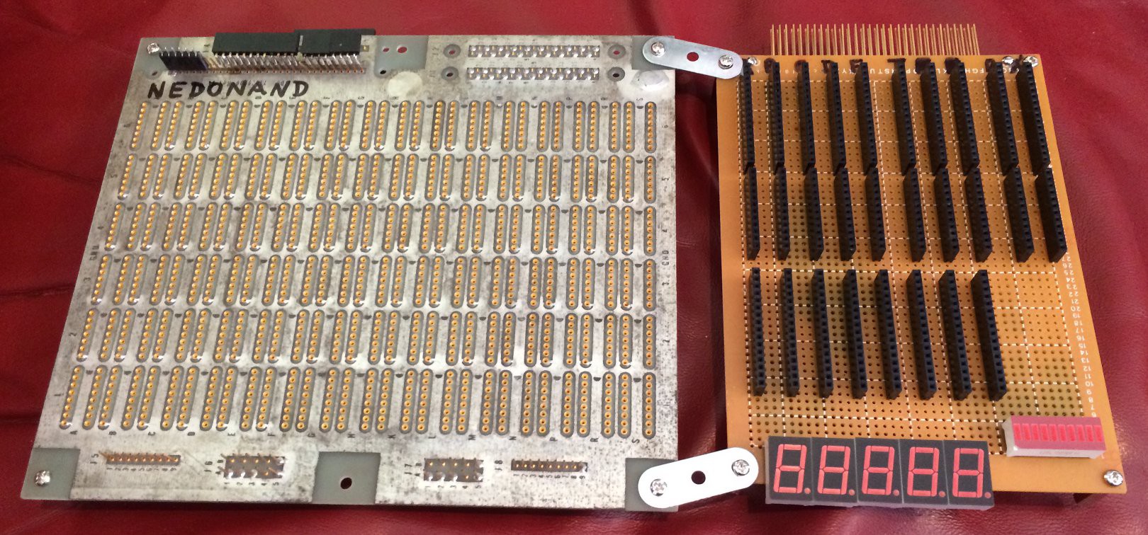
04/17/2016 at 22:10 • 3 commentsThis is a motherboard to connect all parts of NEDONAND together. I decided to use "wire-wrap" technique, but because female header receptacles are relatively new and not exist in wire-wrapping form (with long terminals with square post) I used "side-kick" soldered board where I collect all header receptacles for NEDONAND boards (probably I will need another one to host everything):
![]()
On the top of a side-kick you can see sockets for registers A,B,C,D,E and T (temporary register) and some other things as multiplexers and demultiplexers. Five 7-segment indicators will show registers contents (directly without decoding) for registers A,B,C,D,E and 10-LED bar graph on the right to show content of register F plus 2 additional signals (as ALU usage flag for example). Golden header on the very top of a side-kick is an interface between wire-wrapped universe and soldered universe to make things easier...
-
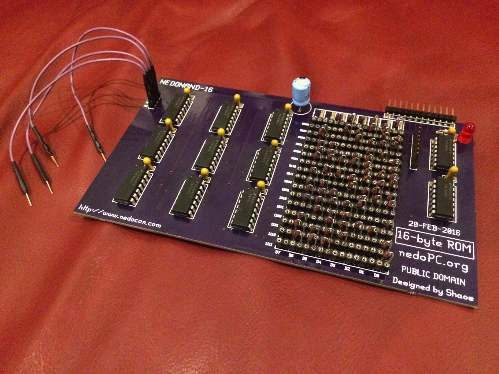
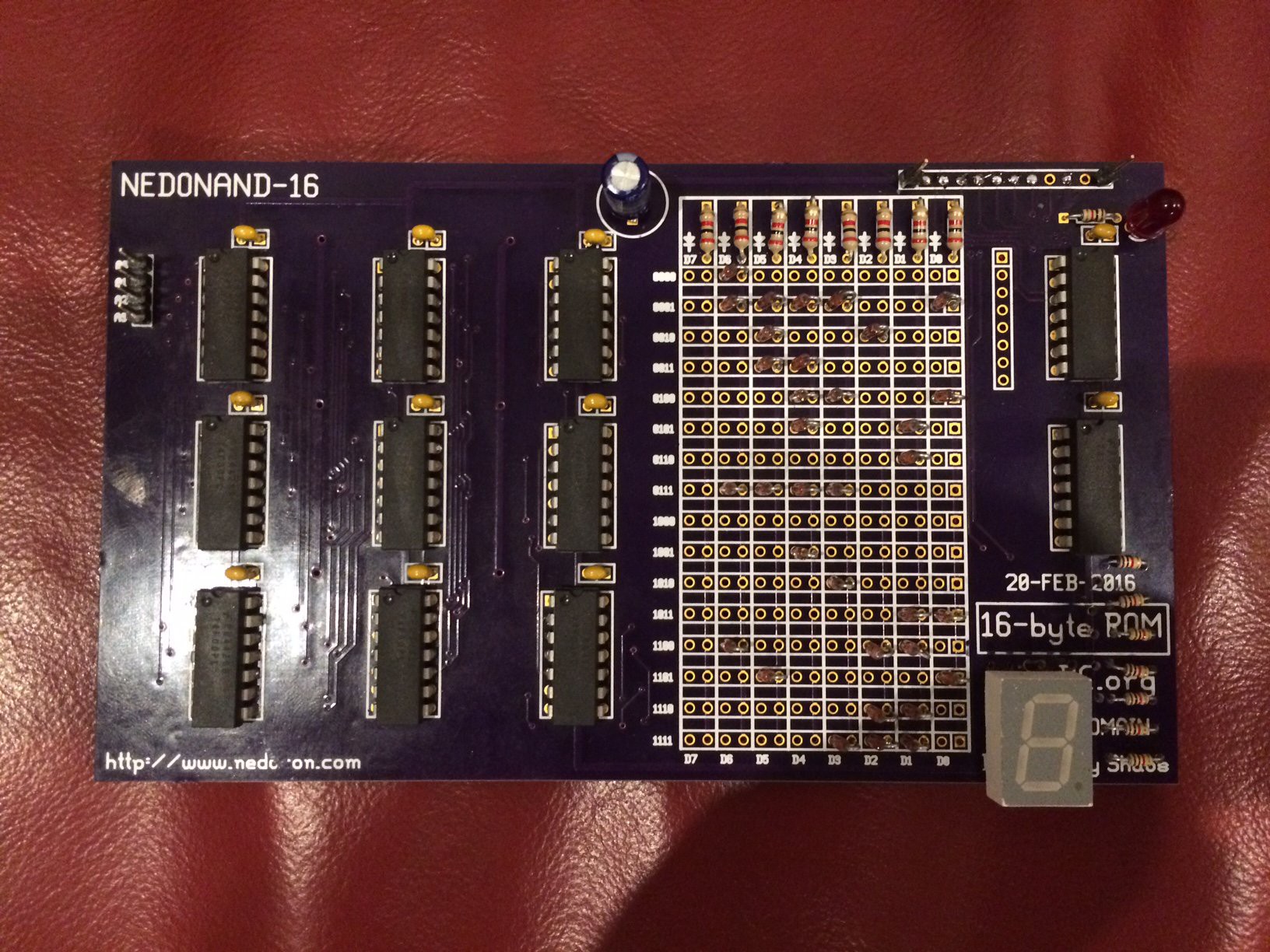
Board NEDONAND-16 tested
04/05/2016 at 04:36 • 2 commentsFinally I completely built and tested NEDONAND-16 board that is MPROM (Manually Programmable Read Only Memory ;)
![]()
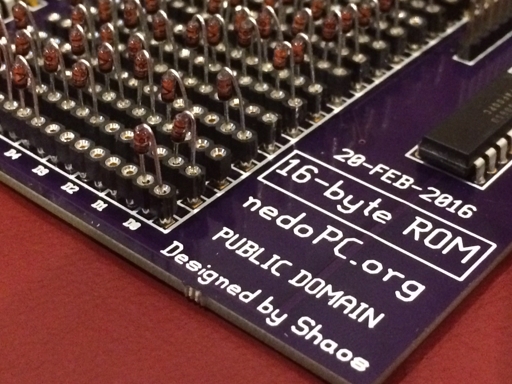
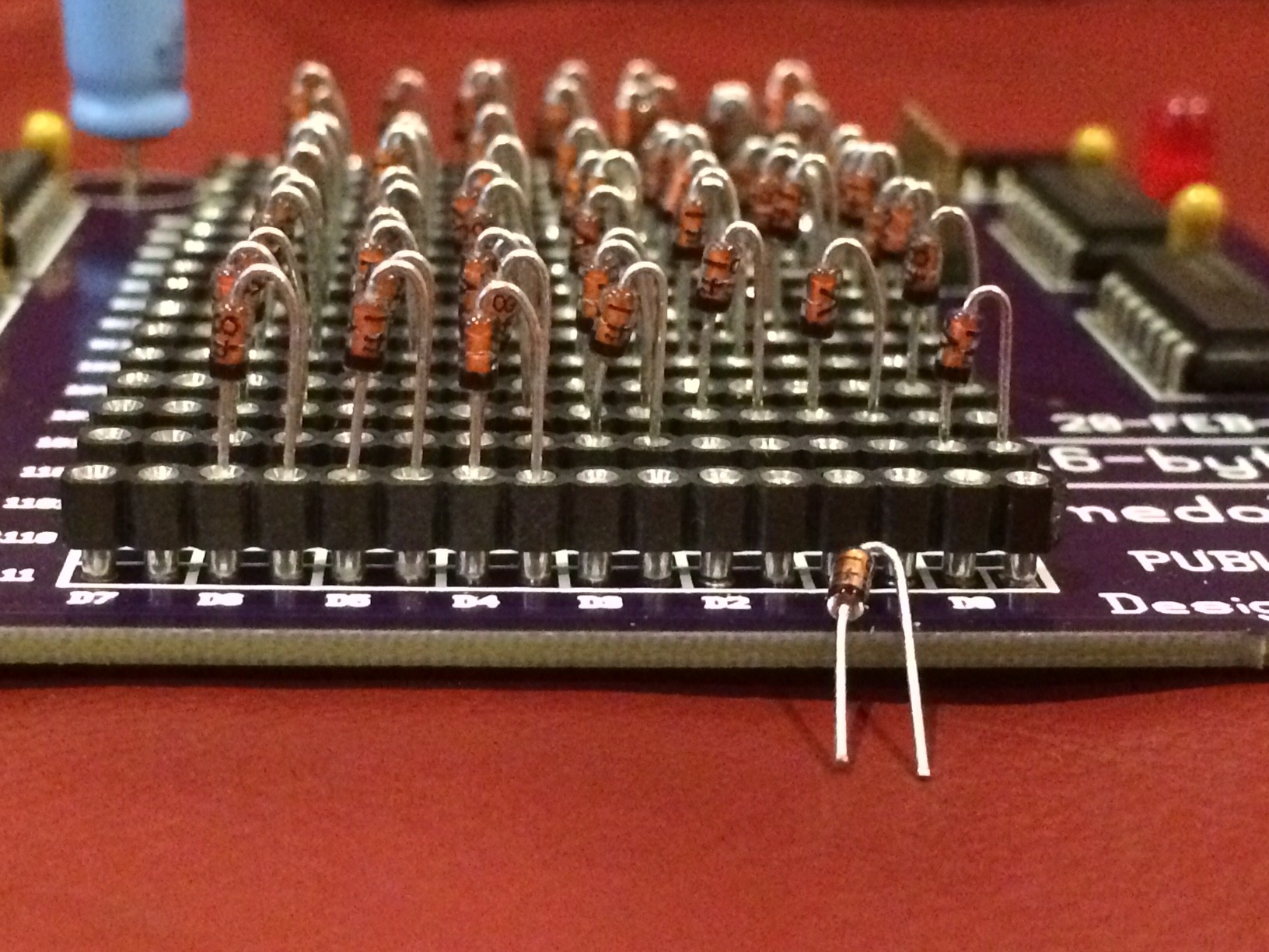
It's programmable by inserting diodes into holes in proper places:
![]()
In order to do that diode's terminals must be specifically formed:
![]()
I connected it to my Analog Discovery 2 and tested its limits in terms of frequency:
![]()
So this is 100 kHz:
![]()
And this is 1 MHz - should be good enough for TTL:
![]()
P.S. But I redo this board anyway, because couple wires still may short on some copies of the board...
-
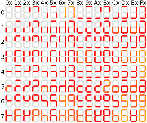
7-segment characters
03/27/2016 at 12:24 • 3 commentsThere is a very useful Wikipedia article about this topic:
https://en.wikipedia.org/wiki/Seven-segment_displayEspecially the table with 128 7-segment "characters" - I put hexadecimal digits around it to make it easier to see what to send to the register to display (and highlighted everything looks like numbers or letters):
![]()
NEDONAND LITE has this table for "characters" with codes from 0x00 to 0x7F - and next 128 characters with codes from 0x80 to 0xFF simply add a dot at the right-bottom corner. Five indicators display content of 5 registers A, B, C, D and E.
-
NEDONAND LITE with HALT mode
03/27/2016 at 01:35 • 0 commentsI added HALT mode into simulation - if any instructions from range 0x80...0x87 is executed (these are placeholders for future RET and RST n) then processor is HALT until user pressed GO button (on the left side of simulation):
![]()
It may help to run large test program when result of every sub-test is displayed on 7-segment indicators with following HALT and when user checked the result he/she may press GO button to run to the next sub-test and so on.
Logisim simulation file was updated: nedonand.circ
P.S. This behavior will still be available even in future full-scale NEDONAND when RET instruction is called from the main program (return stack is empty in this case)
-
NEDONAND lite simulation is ready
03/20/2016 at 12:44 • 0 commentsSimulation of all straightforward commands is ready (everything except RST n, RET, SAEFF and SANFF that require special treatment) with both pipeline stages (2nd stage is having 4-bit ALU that works sequentially in 2 steps to handle 8-bit data). The only special command added is NOP (0x88) and 0xBE,0xBF are still G=F,G=~G. Let's call this subset "NEDONAND lite" - it's pretty much usable even in this state, because bunch of edge-cases mentioned in previous log post was already handled - see Logisim screenshot:
![]()
Interesting thing is that in order to integrate 4-bit ALU (that itself consists of 30 chips 74F00) I added muxing-demuxing logic that consists of about 20 chips 74F00 or 66% of ALU, so it's just a little less than adding 2nd 4-bit ALU in parallel to achieve 8-bit operations. Another observation - having instructions that executed in different stages of instruction pipeline (some in 1st as register copying and some in 2nd as instructions with codes 11xxxxxx that use ALU) is very tricky and require precise edge-case analysis and handling in hardware...
P.S. Expected waveforms for actual hardware (should be slow enough to work with 2716 ROM):
            _________________
/RST ______|
     ______   _   _   _   _
CLK        |_| |_| |_| |_| |_  6.666 MHz
     ______     ___     ___
CLK1       |___|   |___|   |_  3.333 MHz
     ______         _______
CLK2       |_______|       |_  1.666 MHz


1st stage of pipeline (fetch and decode + simple execute):
     __________             _
/OE            |___________|   450 ns
           .        ___    .
REGRD _____________|   |_____  150 ns
           .       .    ___
REGWR _________________|   |_  150 ns

           | 300ns | 300ns |
           ^           ^
           |   450ns   |
           |           \data ready
           |
           \address ready

2nd stage of pipeline (complex execute through ALU):
            _______        .
HALF1 _____|       |_________  300 ns
           .    ___        .
ASTO1 _________|   |_________  150 ns
           .        _______
HALF2 _____________|       |_  300 ns
           .       .    ___
ASTO2 _________________|   |_  150 ns

           | 300ns | 300ns |
P.P.S. If you want to play with it you may download Logisim file from a file storage: nedonand.circ
-
Lets code a little 2
03/19/2016 at 01:42 • 0 commentsow let's code with remembering the fact that we have a pipeline with 2 stages. 3/4 of all instructions (with codes 0xxxxxxx and 10xxxxxx) use only 1st stage, because ALU is doing nothing when they executed - it's A=n, R=~R and R1=R2 including G=R that does jump to new value of program counter (I'm not sure yet about RST/RET and SAEFF/SANFF). Other instructions (with codes 11xxxxxx) use ALU so they took 2 cycles to work and because of that we may have some situations which require special treatment (with special circuitry around). For example, this is subprogram of 16-bit increment:
0) A=E ; no ALU involved on the next step
1) A=A+1 ; ALU will be used on the next step
2) E=A ; copy A to E, but in the same time ALU will change A
3) A=D ; no ALU involved on the next step
4) ADC 0 ; ALU will be used on the next step
5) D=A ; copy A to D, but in the same time ALU will change A
ALU instructions are on 1 and 4 steps. On steps 2 and 5 we have a conflict - A used and modified in the same time. So proposed solution is modify execution of such copy instruction in place - for example here E=A will turn into E=ALU & A=ALU (both registers get ALU output) and D=A will similarly turn into D=ALU & A=ALU. But what if two ALU instructions with A as an argument used one after another:0) RRC A ; on the next step A shifted right 1) RRC A ; on the next step A shifted again (new A stored?) 2) RRC A ; on the next step A shifted again (new A stored?) 3) ... ; here new A stored as a result of previous ALU instruction
Here we have a little conflict, because A will be copied in the same time when it's buffered for ALU - some tricky circuitry should be done in order to fix it. Slightly different situation when we set or clear flag C before ADC and SBC command - everything should work automagically (with flags at least). Another conflicting pair of instructions that will be widely used to calculate AND:0) NAN B ; on the next step ALU should calculate ~(A&B) 1) A=~A ; here A must be inverted and stored from ALU in the same time
In this case we should execute storing to A - not direct, but inverted! Next one - what if A is modified immediately after instruction with ALU? For example:
0) NAN B
1) A=B
Here ALU output must be ignored (only flags will be used). Accumulator will get value from B at the end on step 1 and not ~(A&B). But if it's direct modification of F:0) NAN B 1) F=0
then most likely we should use flags from ALU, but PC-bits from instruction... -
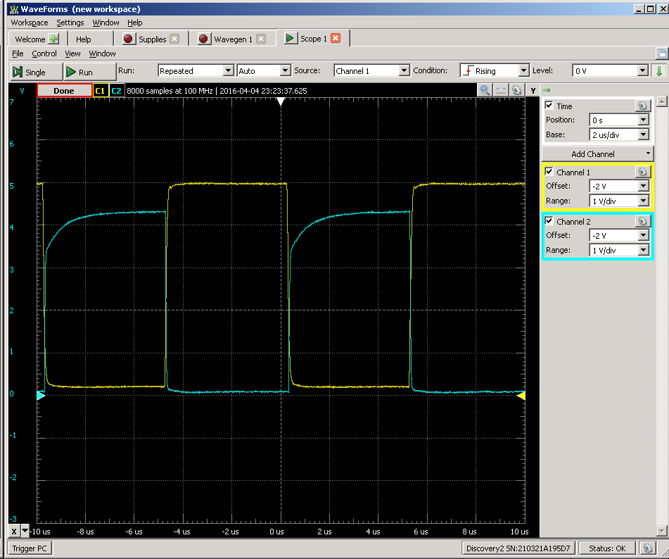
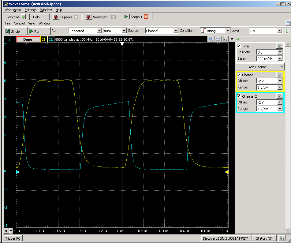
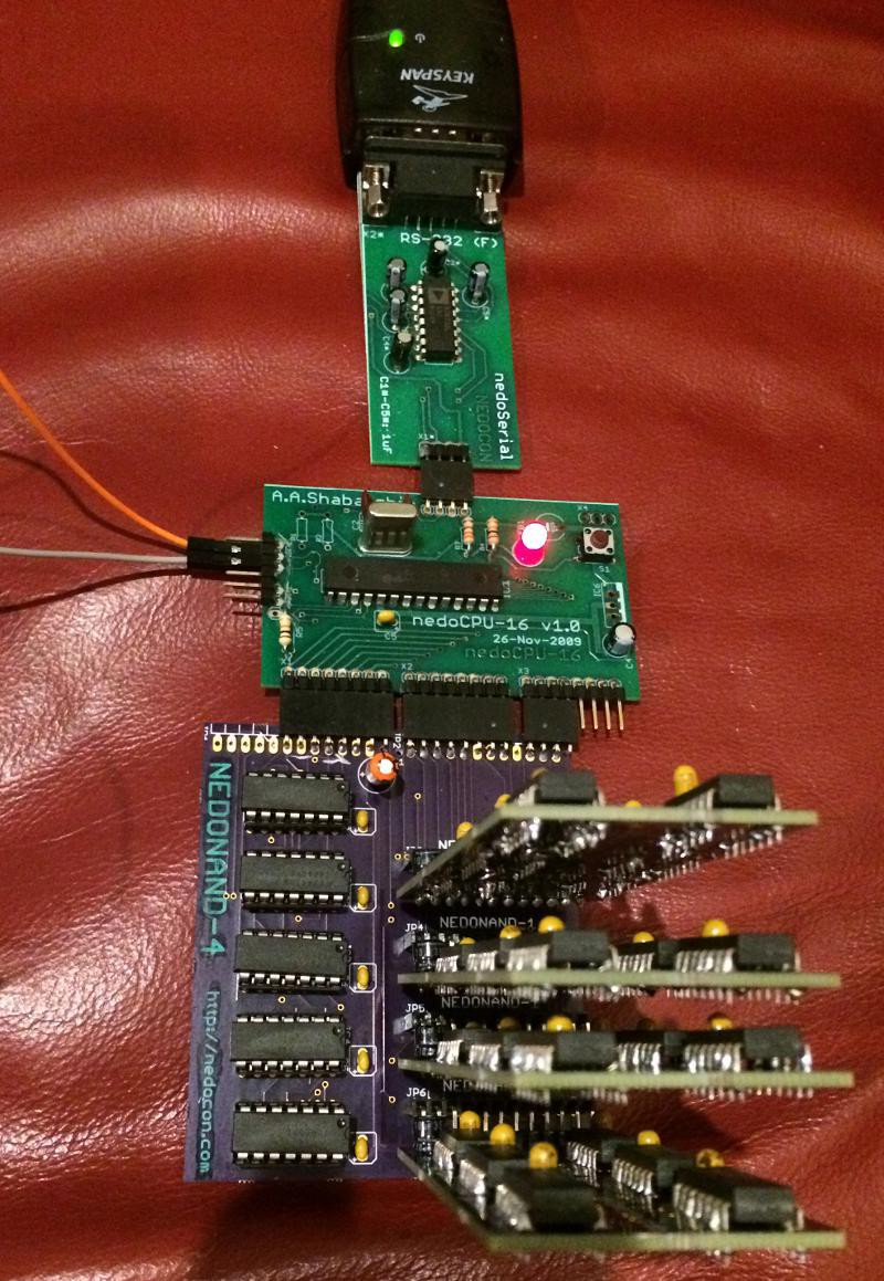
ALU tested by PIC
03/15/2016 at 23:28 • 0 commentsToday I successfully tested assembled 4-bit ALU (previous revision of NEDONAND-4 board with four NEDONAND-1 connected). In order to do this I slightly modified the board to connect nedoCPU-16 with it:
![]()
![]()
Then I wrote a simple program in PIC assembler that worked above PDBL (my Public Domain Boot Loader) to communicate with PC through good old RS-232. Program sent 4096 variants of input vectors (stressing ALU a little before every vector) and sampled output with delays 200ns, 600ns, 1.0us, 1.4us and 1.8us with logging every value:
![]()
Then I wrote C-program that analyze collected logs (see logs) and print report with incorrect values - it's appeared that some ADD operations were not be able to finish in 200ns, but all finished in 600ns (modified program collected 400ns moment also and all finished in 400ns as well - see logs). So ALU worst performance metrics are located somewhere between 200ns and 400ns. This is a little worse than I theoretically calculated using 74F00 spec - I expected 120ns delay (200ns in worst case if all chips have max allowed propagation delay 5ns), but in reality it's somewhere in 200...400ns range. Incorrect samples (here [0] means 200ns after inputs changed):
ADD 0EC[0] 3F a=-2 b=0 c=1 -> d=-1 (15) c=0 (1) v=0 (1)
ADD 0ED[0] 3F a=-2 b=0 c=1 -> d=-1 (15) c=0 (1) v=0 (1)
ADD 0EE[0] 3F a=-2 b=0 c=1 -> d=-1 (15) c=0 (1) v=0 (1)
ADD 0EF[0] 3F a=-2 b=0 c=1 -> d=-1 (15) c=0 (1) v=0 (1)
....
ADD F8C[0] 03 a=-8 b=-1 c=1 -> d=-8 (0) c=1 (1) v=0 (1)
ADD F8D[0] 03 a=-8 b=-1 c=1 -> d=-8 (0) c=1 (1) v=0 (1)
ADD F8E[0] 03 a=-8 b=-1 c=1 -> d=-8 (0) c=1 (1) v=0 (1)
ADD F8F[0] 23 a=-8 b=-1 c=1 -> d=-8 (8) c=1 (1) v=0 (1)
See full output here. So most of the time it's incorrect most significant bit and/or flags C/V (carry and overflow). And as I said at 400ns everything is correct. Inputs are in formats BBBBAAAACOOO (12-bits represented by 3-digit hexadecimal number before [0]). Outputs are in format DDDVC (5-bits represented by 2-digit hexadecimal number after [0]). Then numbers in parentheses show actual numbers from the board...
P.S. All source codes are available on GitLab (since June 2018):https://gitlab.com/nedopc/nedonand/tree/master/tester/preliminary
-
All boards received
03/12/2016 at 03:52 • 0 commentsThe rest of the boards just came:
![]()
I think I will connect them together through wire-wrapped "motherboard" (lets call it "NEDONAND-10" ; )
All of these NEDONAND components could be tested one by one using PIC microcontroller (connected to PC through RS-232) and one 30-pin socket:
    NN1  NN2  NN3    NN4   NN5  NN6  NN7  NN8  NN9  NN16
--------------------------------------------------------
 1) GND  GND  ---    GND   GND  GND  GND  GND  GND  GND
 2) O0   D1   ~Q0    D0    D0   O0   O0   I0   A    D0
 3) O1   ^C1  ~Q1    D1    D1   O1   O1   I1   B    D1
 4) O2   /R1  ~Q2    D2    D2   O2   O2   I2   C    D2
 5) A    Q1   ~Q3    D3    D3   O3   O3   I3   D    D3
 6) B    /Q1  IN     COUT  D4   O4   O4   I4   E    D4
 7) C    D2   ACT0   VOUT  D5   O5   O5   I5   F    D5
 8) H    ^C2  ACT1   /O0   D6   O6   O6   I6   G    D6
 9) L    /R2  /RESET /O1   D7   O7   O7   I7   H    D7
10) COUT Q2   CLK    /O2   STB  SEL  /ENO OUT  I    NC (/OE)
11) DOUT /Q2  NC     /ZERO NC   /SEL EN   NC   AND  NC (/CS)
12) VCC  VCC  VCC    VCC   VCC  VCC  VCC  VCC  VCC  VCC
13) ---  ---  GND    ---   ---  ---  GND  GND  ---  ---
14)                                  A0   A0        ~A0
15)           D0     O0    Q0   A0   A1   A1        ~A1
16)           D1     O1    /Q0  B0   A2   A2        ~A2
17)           D2     O2    Q1   A1                  ~A3
18)           D3     C     /Q1  B1
19)           D4     A0    Q2   A2
20)           D5     A1    /Q2  B2
21)           D6     A2    Q3   A3
22)           D7     A3    /Q3  B3
23)           D8     B0    Q4   A4
24)           D9     B1    /Q4  B4
25)           D10    B2    Q5   A5
26)           D11    B3    /Q5  B5
27)                        Q6   A6
28)                        /Q6  B6
29)                        Q7   A7
30)                        /Q7  B7
-
Another test
03/10/2016 at 05:57 • 2 commentsJust put together NEDONAND-3 with 2 NEDONAND-2 and NEDONAND-16 ROM "programmed" with 4-bit to Hex converter to display 4-bit address in human readable format:
This is ROM alone (I drilled a few holes and installed 7-segment indicator directly on the board):
![]()
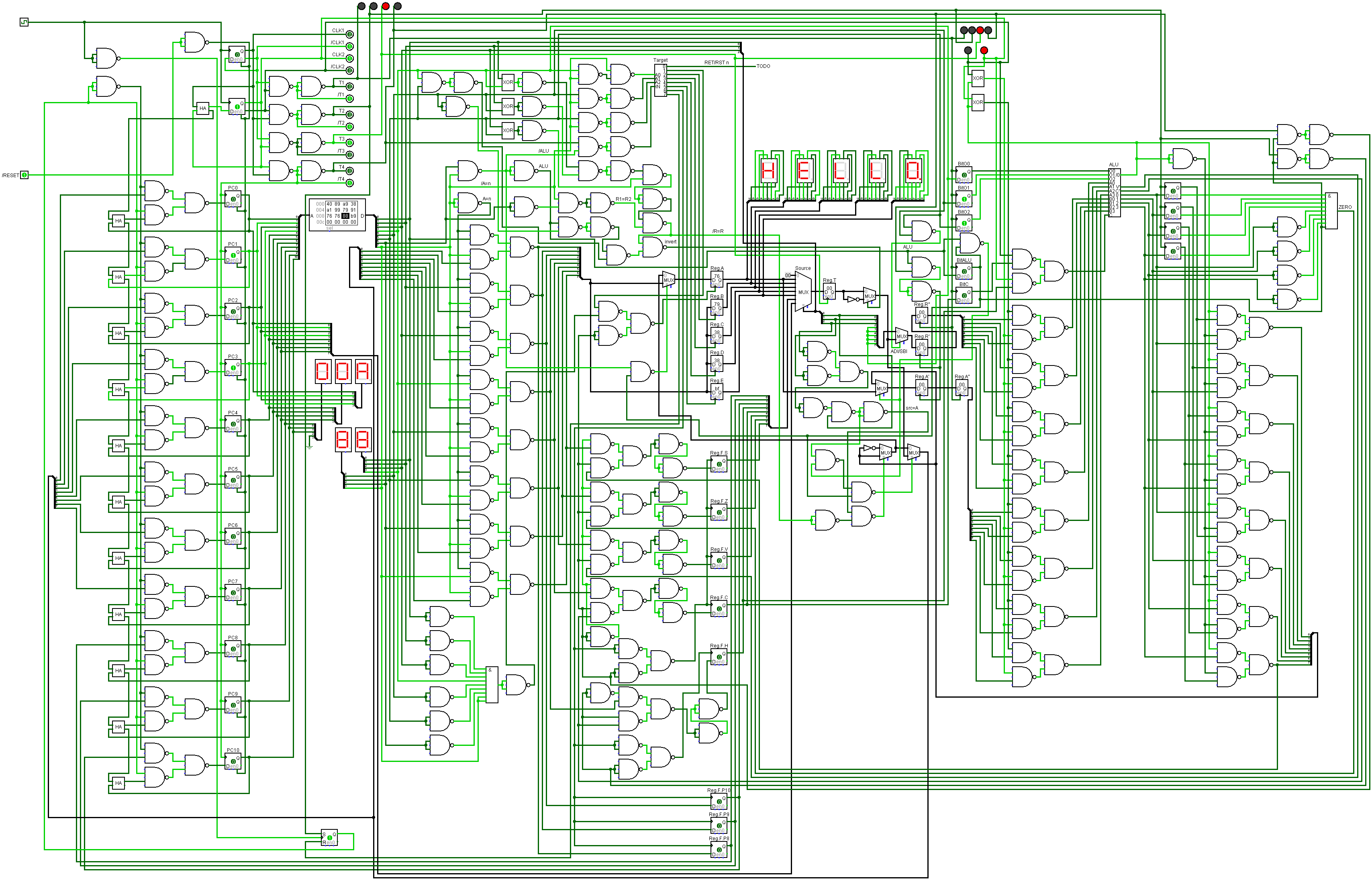
NEDONAND homebrew computer
NEDONAND is 8-bit homebrew computer entirely built out of many 74F00 chips (2-input NAND gates)