SHAOS
SHAOS-
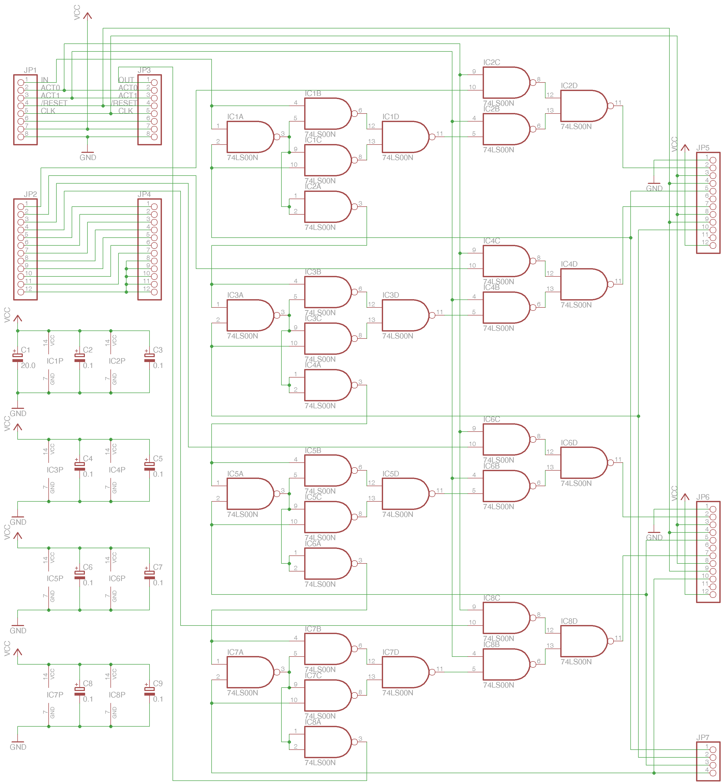
Board NEDONAND-3
02/24/2016 at 02:25 • 1 commentNEDONAND-3 is 4-bit part of NEDONAND program counter that uses 2 board NEDONAND-2
![]()
Pins description (2 rows - male for inputs and female for outputs):
1.1) IN (OUT) - count enable
1.2) ACT0 - external writing signal "0"
1.3) ACT1 - external writing signal "1"
1.4) /RESET - master reset
1.5) CLK - clock signal
1.6) NC - not connected
1.7) VCC - power +5V
1.8) GND - ground2.1) D0 - bit 0 for writing
2.2) D1 - bit 1 for writing
2.3) D2 - bit 2 for writing
2.4) D3 - bit 3 for writing
2.5) D4 - used in next stacked boards
2.6) D5 - used in next stacked boards
2.7) D6 - used in next stacked boards
2.8) D7 - used in next stacked boards
2.9) D8 - used in next stacked boards
2.10) D9 - used in next stacked boards
2.11) D10 - used in next stacked boards
2.12) D11 - used in next stacked boards (in case of 2K memory it's "0")This board could be used as a single one for 16-byte program memory or as stacked together up to 3 (to use all 2048 bytes that is max by NEDONAND spec and D11 might be counter overflow flag):
![]()
-
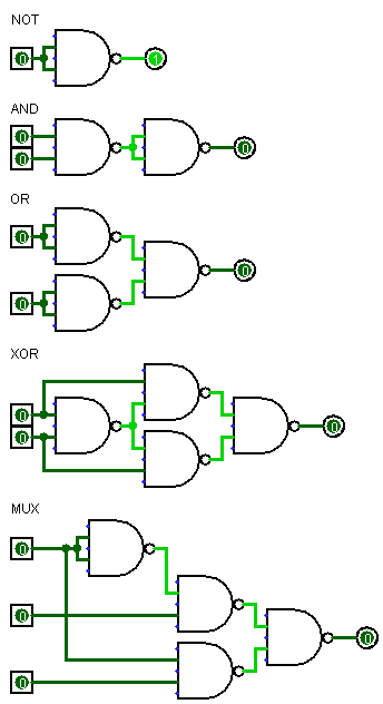
Basic NANDology ;)
02/22/2016 at 03:23 • 0 commentsIt is known fact that using just NAND-gates it's possible to build everything else (so NEDONAND should prove it). For now I can show some basic things - getting NOT, AND and OR from NANDs is kind of obvious excercise:
![]()
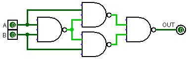
Last one is not so obvious - it's 2:1 multiplexer (that could be used to build bigger ones) - most used building block in NEDONAND. Now very recognizable XOR circuit:
![]()
And it could be extended to be a true "half-adder":
![]()
And finally, already mentioned before transparent D-latch:
![]()
This is it for the first lesson of NANDology from Shaos ;)
-
2 first boards are ready
02/22/2016 at 03:07 • 0 comments![]()
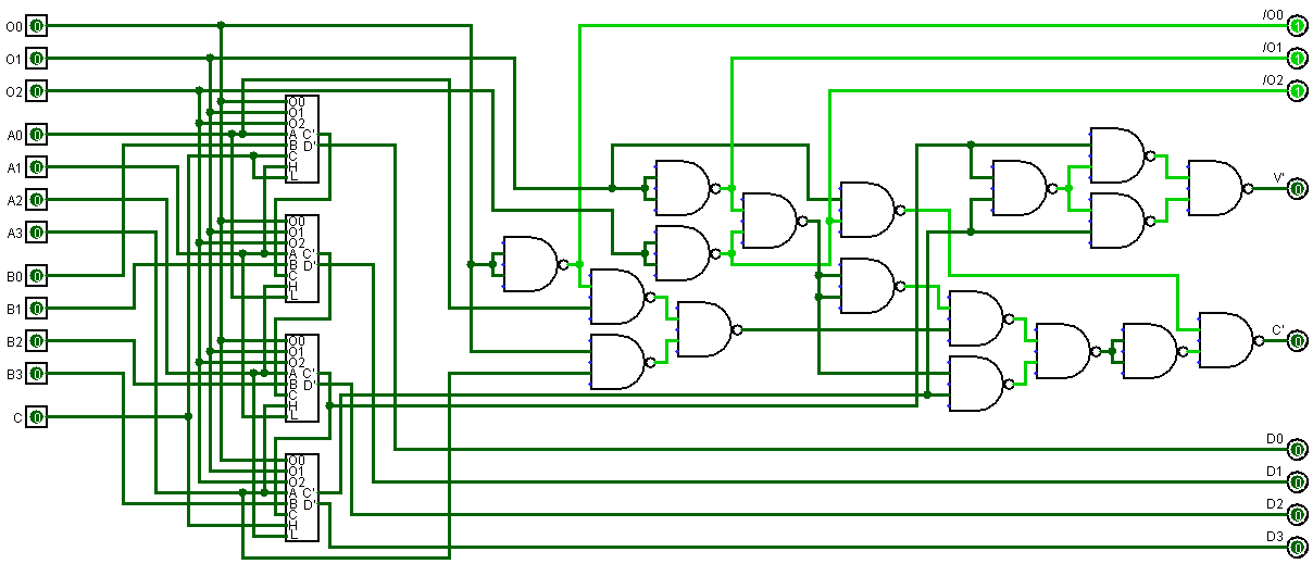
4-bit ALU could be built from 4 ALU slices (NEDONAND-1 board from above):
![]()
Here you can see carry out C and overflow V flags formation (C is always 1 with logical operations)
-
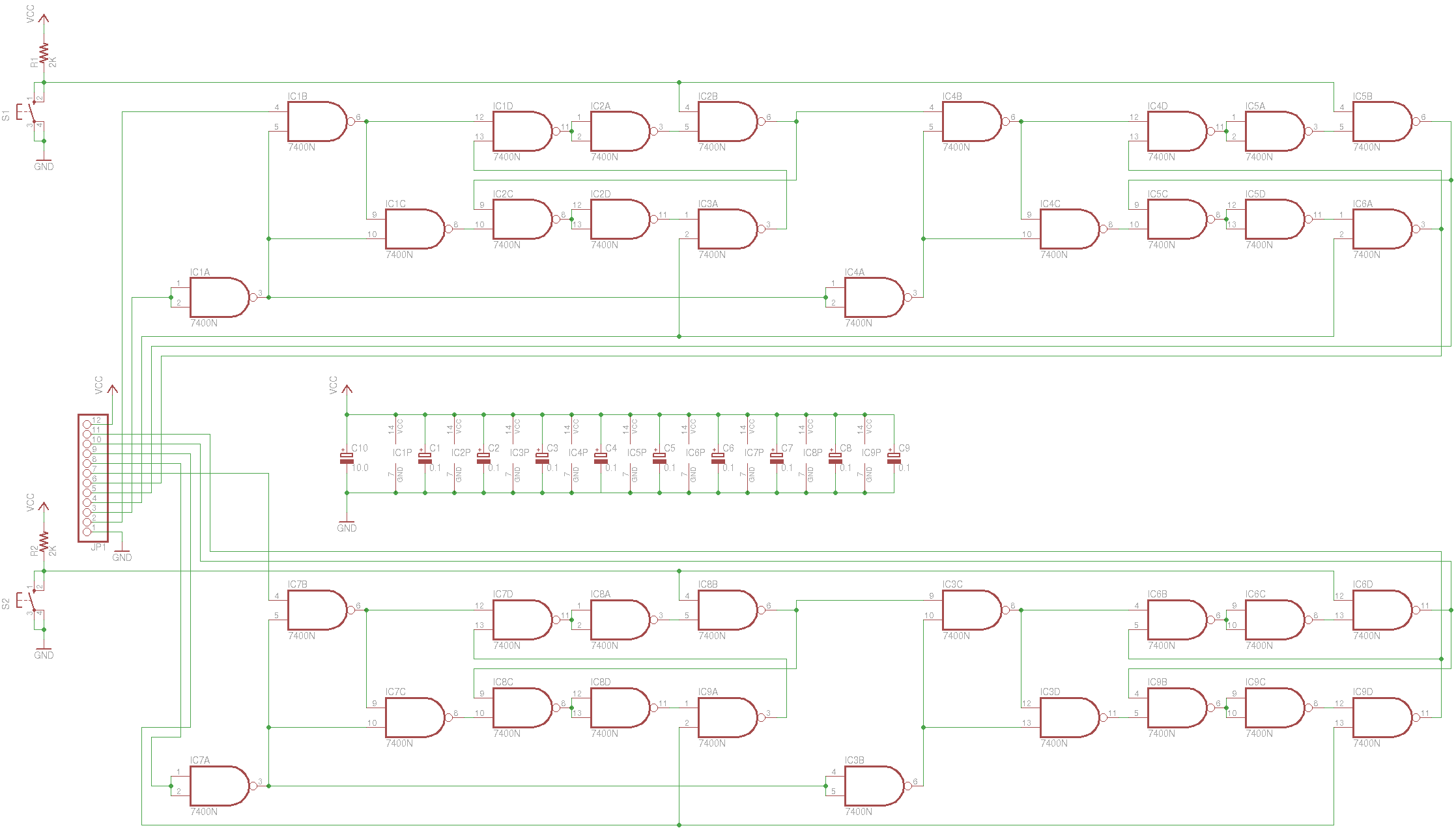
Board NEDONAND-2
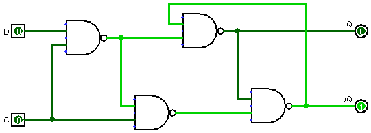
02/22/2016 at 02:57 • 0 commentsNow we need D-trigger. Simplest possible one is this:
![]()
Problems: it's transparent (when C is "1" then Q transparently outputs value from input D) and there are no ability to clear it besides D/C. So we will use more sophisticated one - this board has 2 of them (it's like functional analog of 7474 chip, but with buttons for set):
![]()
Pins description (from right to left):
1) GND - ground;
2) D1 - first data input;
3) ^C1 - first clock input (front active);
4) /R1 - first reset input;
5) Q1 - first straight output;
6) /Q1 - first inverted output;
7) D2 - second data input;
8) ^C2 - second clock input (front active);
9) /R2 - second reset input;
10) Q2 - second straight output;
11) /Q2 - second inverted output;
12) VCC - power +5V.![]()
-
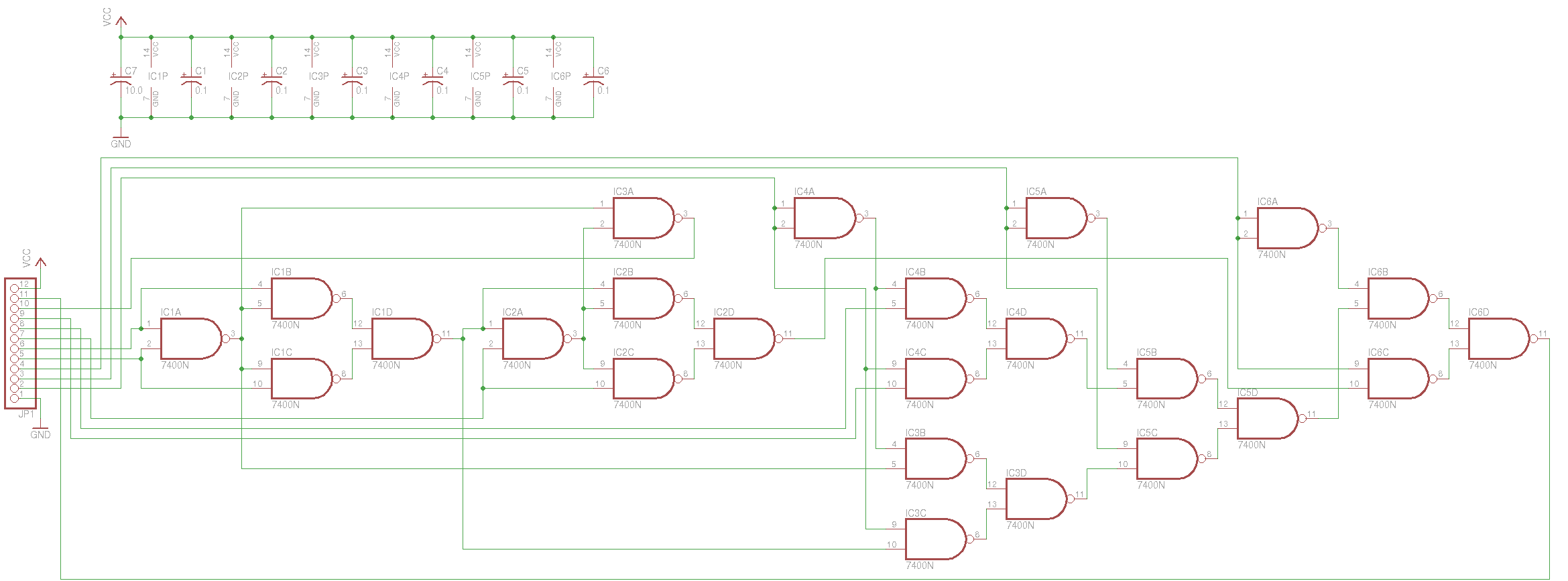
Board NEDONAND-1
02/22/2016 at 02:45 • 2 comments1st board for this project is NEDONAND-1 that is 1-bit slice of NEDONAND ALU:
![]()
Pins description:
1) GND - ground;
2) O0 - bit 0 of ALU operation;
3) O1 - bit 1 of ALU operation;
4) O2 - bit 2 of ALU operation (if it's "1" then O0 and O1 are ignored);
5) A - input bit A (always from accumulator);
6) B - input bit B (might be from register or number);
7) C - input bit C (carry);
8) H - higher bit for rotation right;
9) L - lower bit for rotation left;
10) COUT - carry out;
11) DOUT - data out;
12) VCC - power +5V.![]()
NEDONAND homebrew computer
NEDONAND is 8-bit homebrew computer entirely built out of many 74F00 chips (2-input NAND gates)