robert.c.baruch
-
Quick update: 10-tube test
07/23/2016 at 18:44 • 0 commentsI decided to use a Raspberry Pi 3 to run the display, and tested it using a simple program that uses WiringPi.
Since I'm pretty confident that all the hardware works, I'll be focusing on the software now.
-
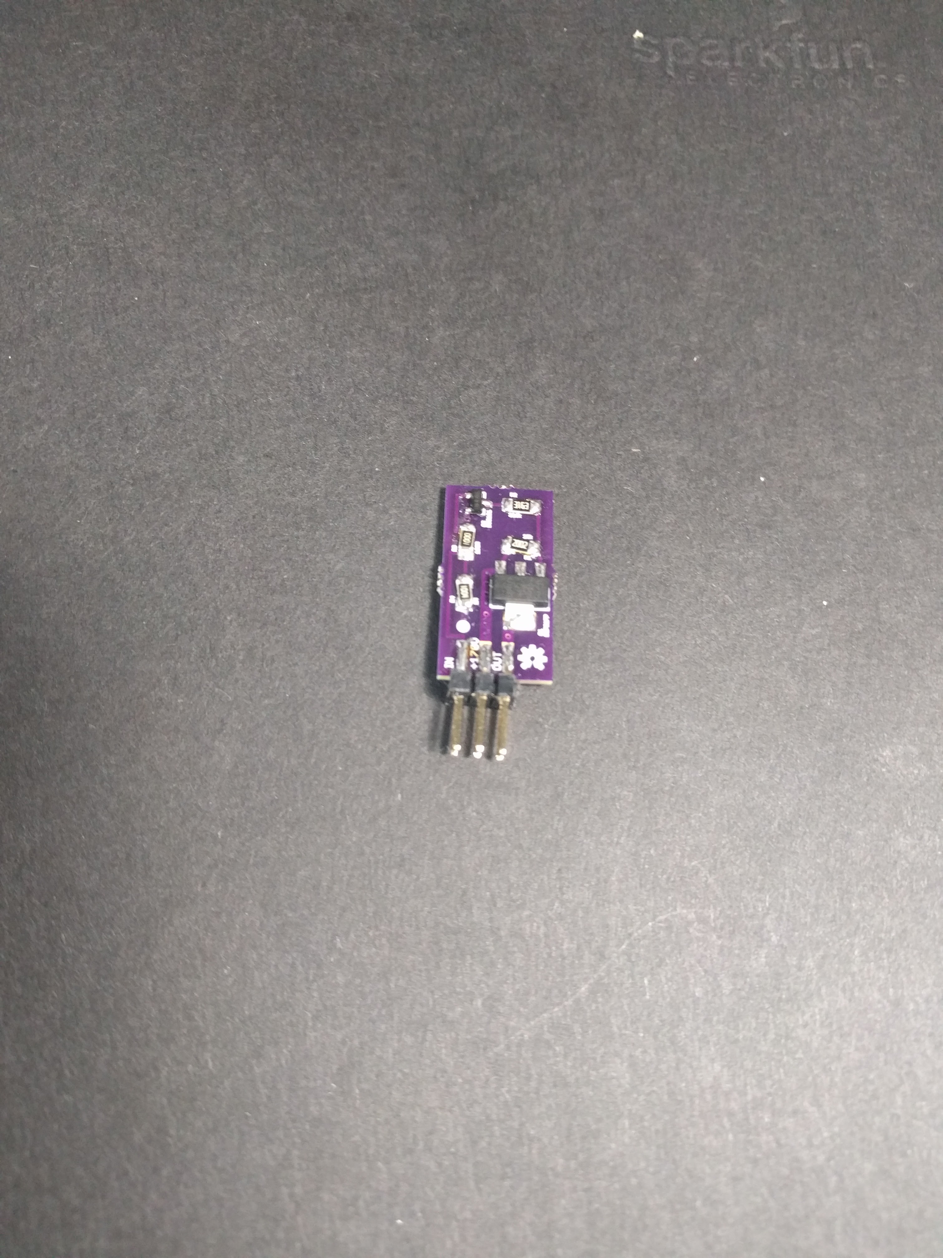
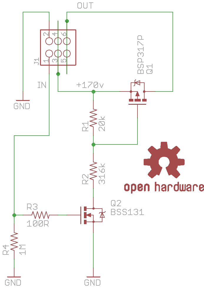
High side switch
06/20/2016 at 22:02 • 0 commentsPreviously I mentioned that I needed a high-side switch that the processor could control to enable +170VDC power to the Nixies when it was ready. I prototyped it 2 weeks ago, but it wasn't until today that OSHPark came back with the boards. I didn't make it breadboard-compatible, since it's just intended to be a little module.
It must have +170VDC to switch or else the voltage divider for the high-side MOSFET doesn't give the gate the right voltage. But then you can use 3v3 or 5v to turn it on.
Eagle and Gerber files in the Files section.
![]()
![]()
-
Keyboard
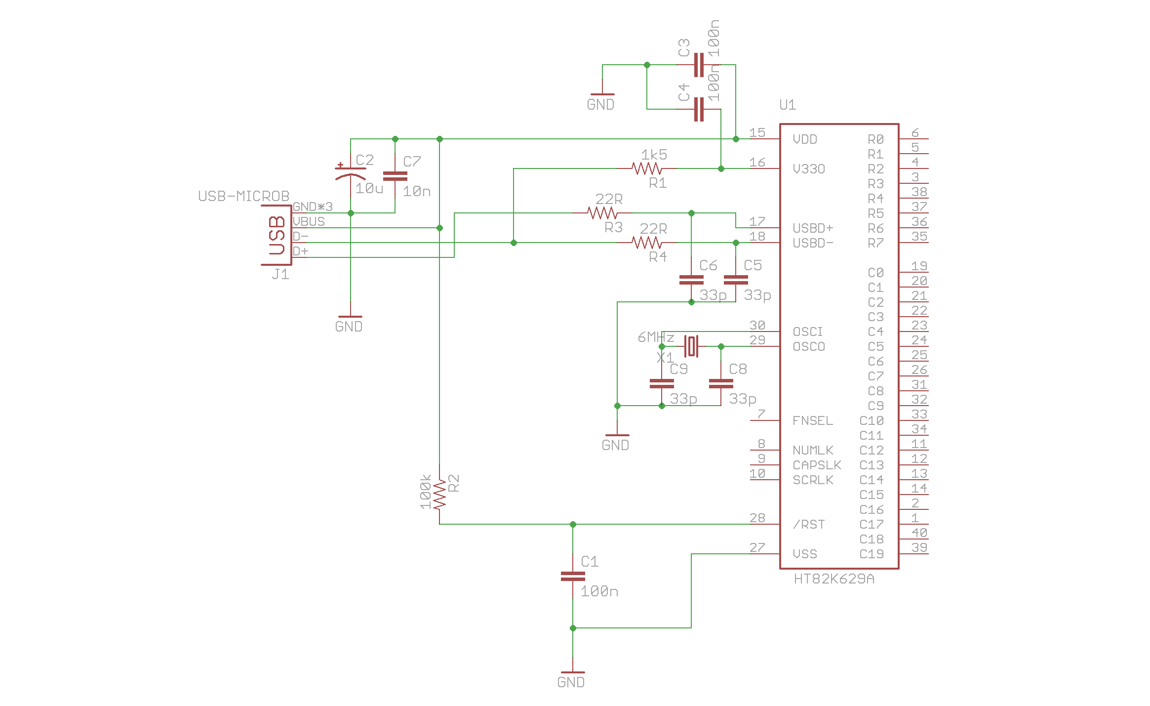
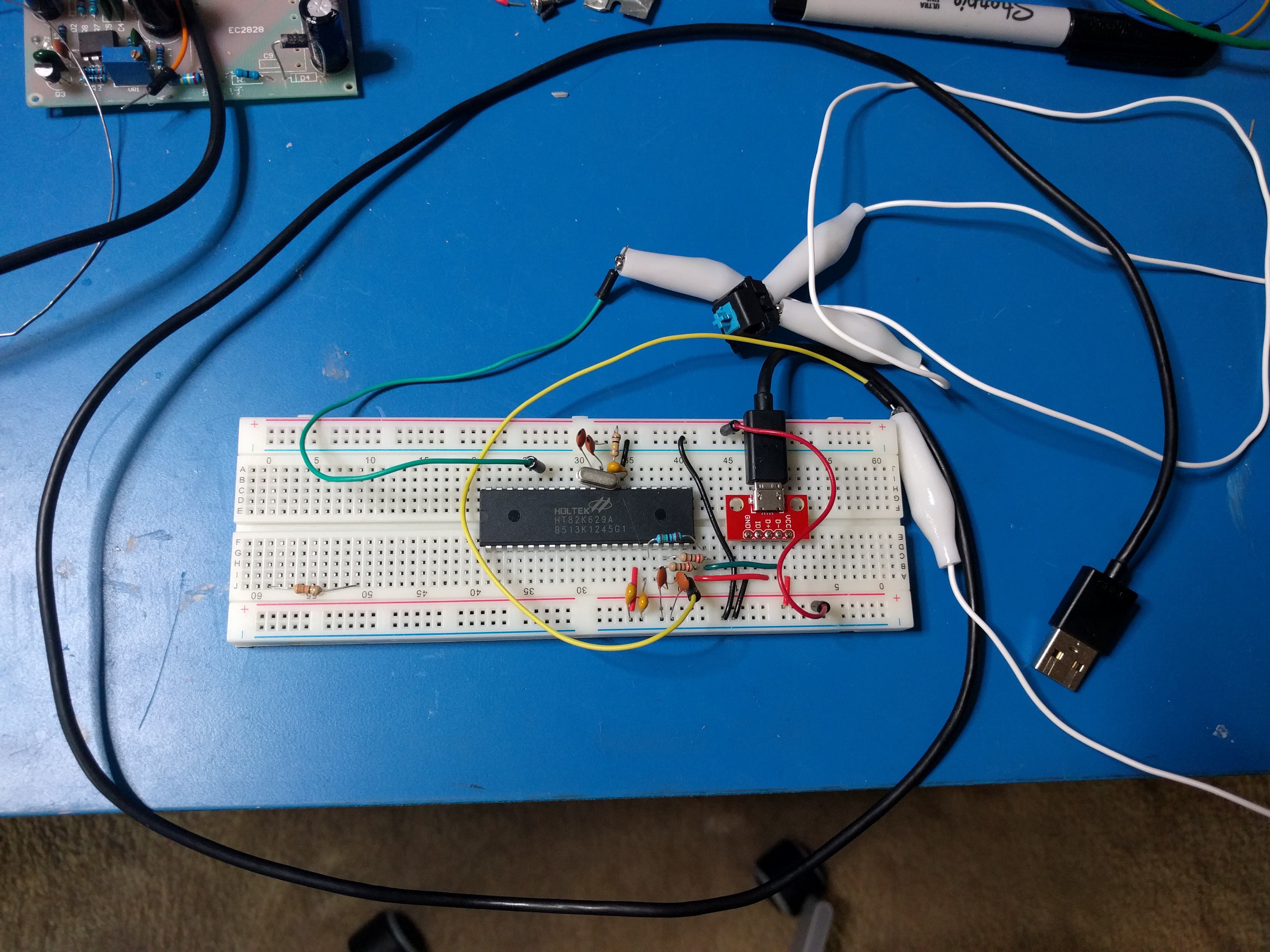
06/02/2016 at 02:34 • 2 commentsI found a cheap USB keyboard controller chip! It is the Holtek HT82K629A. It requires a minimum of passives, plus a 6MHz crystal, and you're done -- just hook it up to USB and it looks like a standard keyboard.
![]()
You don't get to say which key is which: a given intersection of row and column is hardwired to be a given key. I've hooked up the "1" key. When I plug it in to my computer, it works great. I can type 1's all day. So now I don't need an FRDM board to run the keyboard.
![]()
-
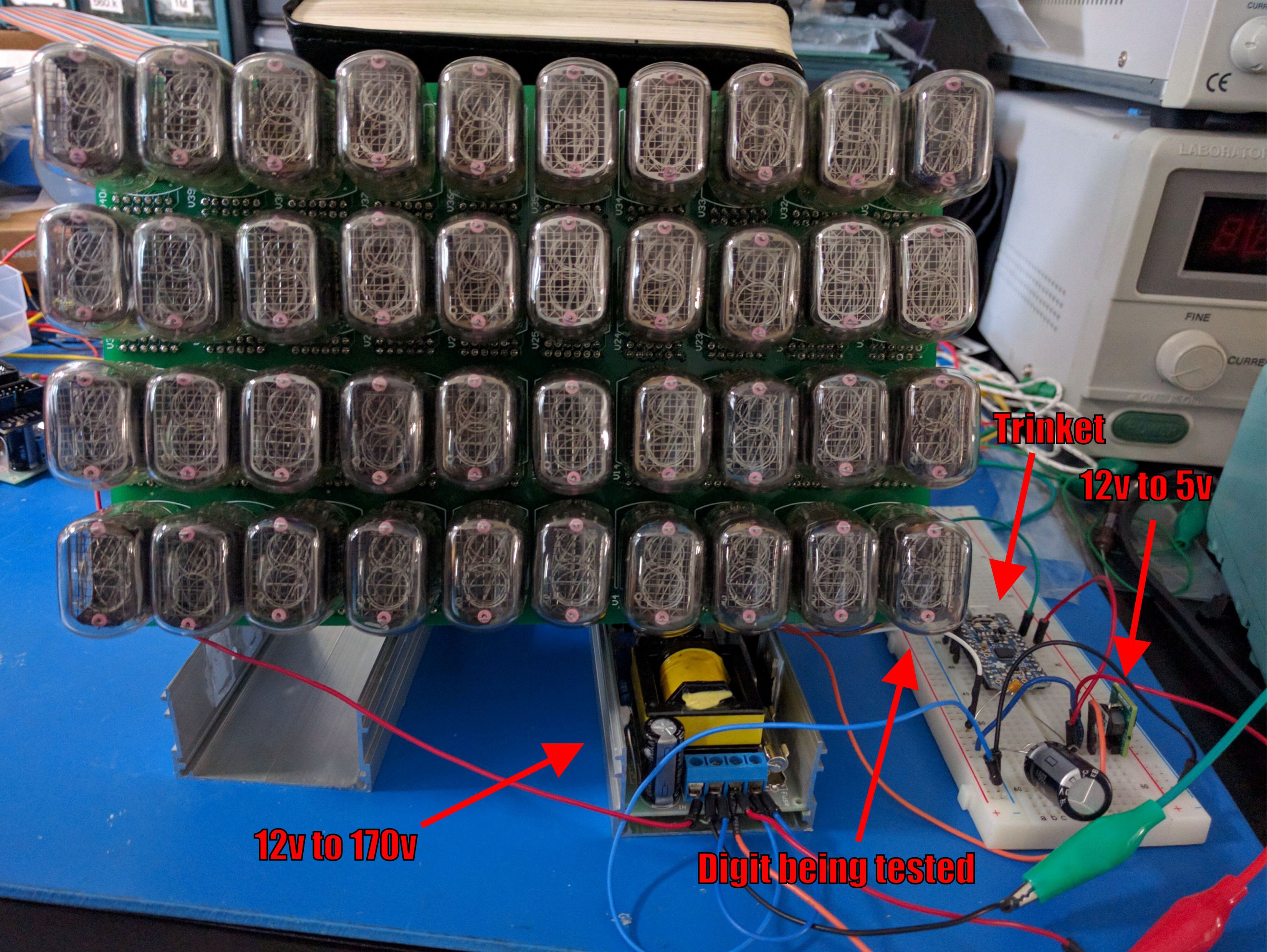
Initial testing of the driver board
05/28/2016 at 20:52 • 0 commentsWith the high voltage power supply sorted out, I wrote a quick Arduino sketch for an Adafruit 5V Trinket Pro to drive one Nixie digit via the pseudo-SPI. I am using a Murata OKI-78SR-5/1.5-W36-C 3-terminal DC/DC converter to convert the 12V input power supply to 5V for the Trinket and the driver board.
Normal SPI has clock and data, plus a slave select line which goes low before transmitting data, and high after the transmission is done. However, the VFD driver requires a latch pulse after the transmission is completed to latch the clocked-in data to the output buffers. Also, there is no slave select line.
The sketch goes through all the digits, and adds the latch pulse at the end of every transmission.
![]()
Note that there's a problem. When the thing powers up, the default state of the VFD driver output is low, which turns on a digit. Well, with all outputs at low, all digits are on until the Trinket starts and sets the state properly.
I will probably need a switch to disable the 170v line until the controller is ready.
-
China 1 Rob 0
05/22/2016 at 00:18 • 0 commentsYeah, I couldn't get the boost converter I designed to work. It was fine up to about 4 mA out, but then the voltage would sag.
Rather than waste time on chasing down why the circuit doesn't work, I'll just stick with the power supply from China. It works.
-
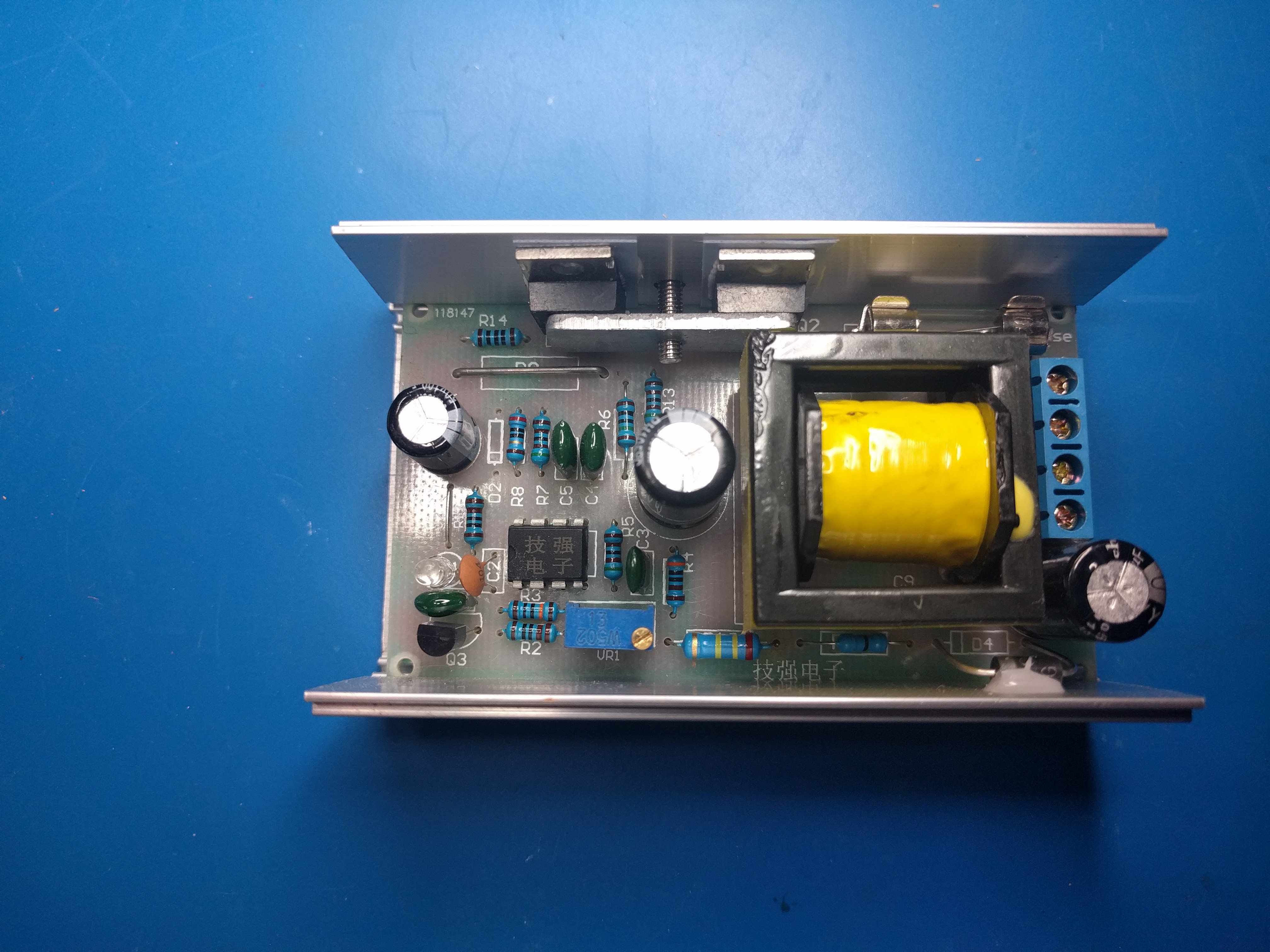
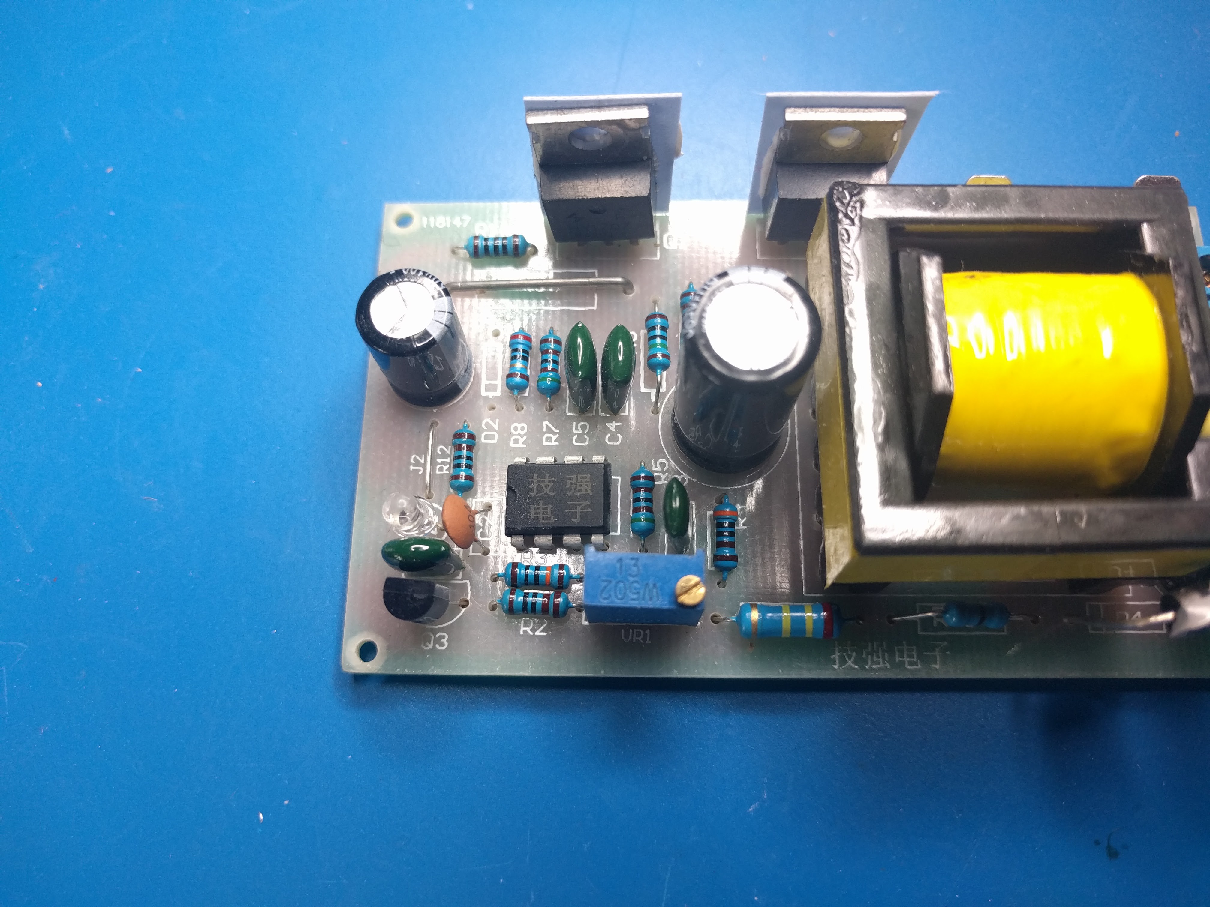
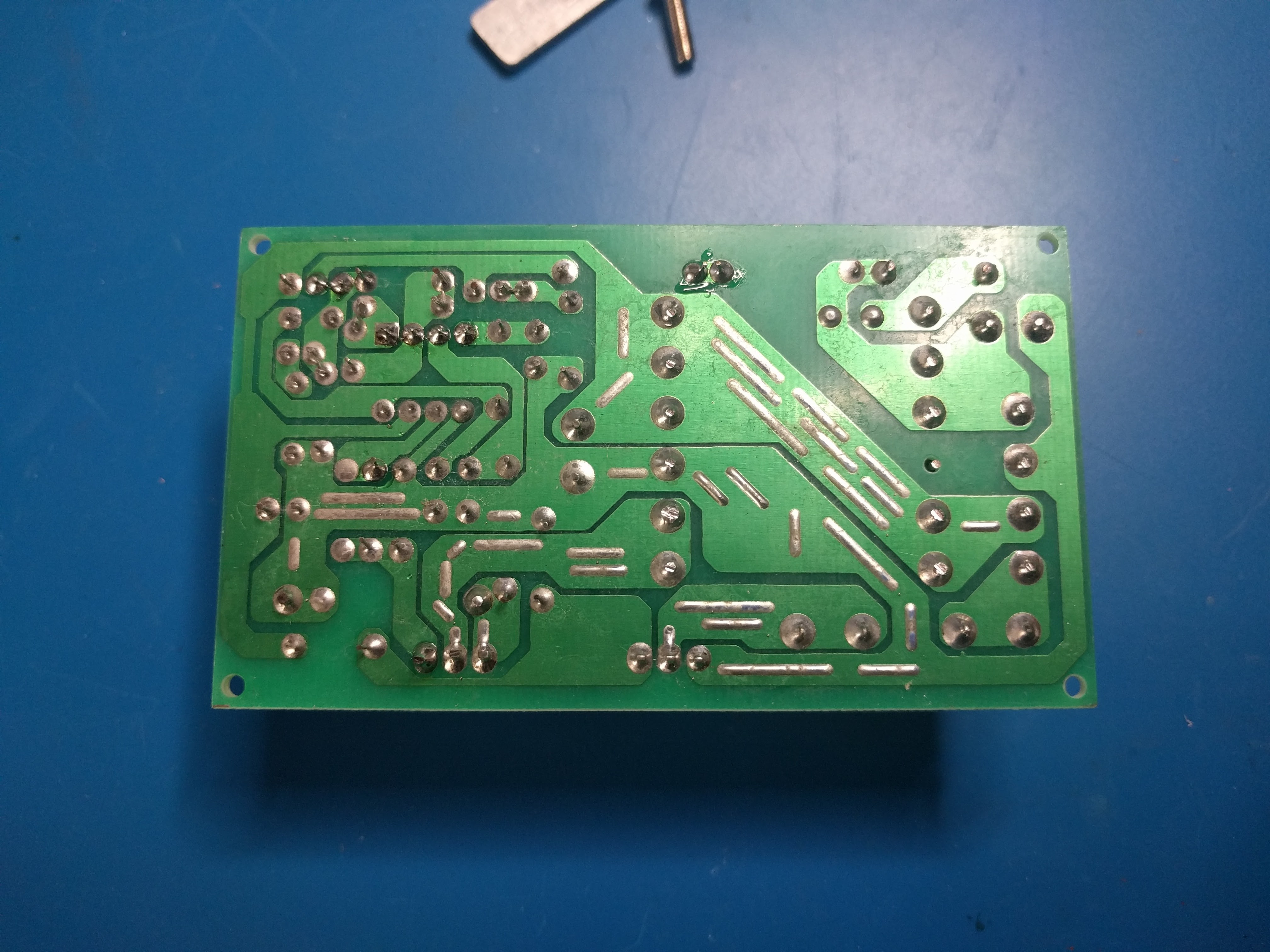
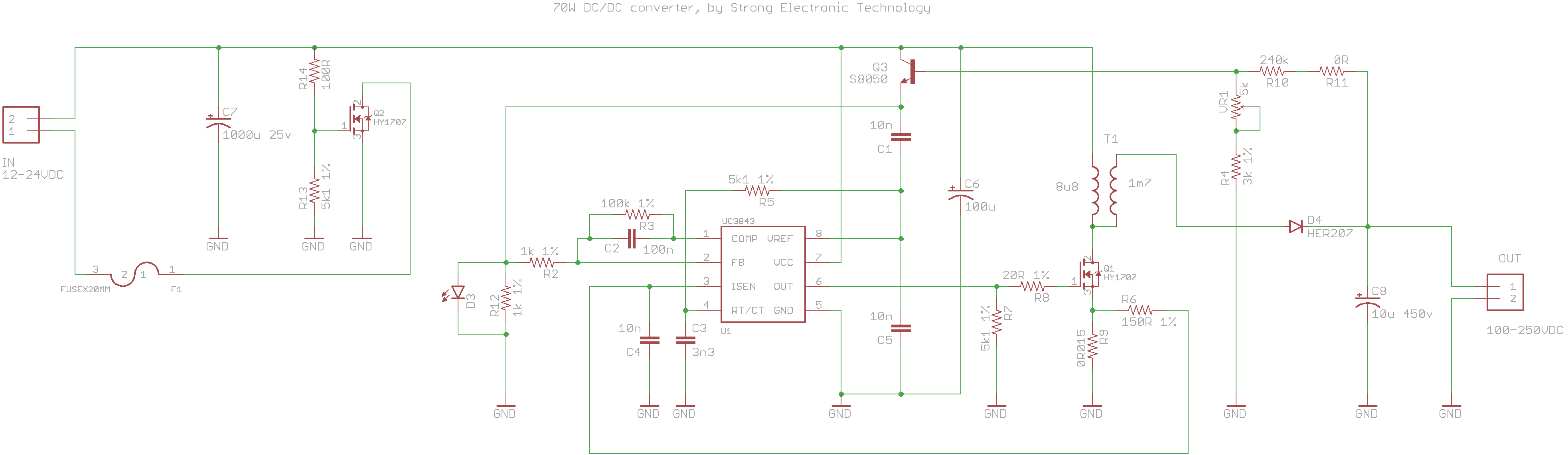
Reverse engineered boost converter
05/19/2016 at 02:53 • 12 commentsSo I got the Chinese DC/DC converter, and it seems to work. Powered with 12VDC and set for 170VDC loaded with 150mA, efficiency is 75%.
![]()
The chip, as well as the board, is labelled with the Chinese for "Strong Electronic Technology". Note the two heatsinked MOSFETs. The switching diode is in the lower right.
I didn't turn it on, I took it apart first.
![]()
![]()
The schematic (click to embiggen):
![]()
(Updated to show a transformer T1 instead of a single inductor. It probably has a turns ratio of 1:14, but I won't be sure unless I sacrifice the transformer and unwind it. Also corrected the current sense circuit.)
The bright minds over at the eevblog forum identified the chip from its topology as the UC3843 SMPS controller.
The only weird thing here is that input MOSFET. It appears to be for reverse input polarity protection. A MOSFET and two resistors when a single diode would do. I must not be seeing something.
In any case, now that I designed my own, with fewer parts, maybe I can get better efficiency?
-
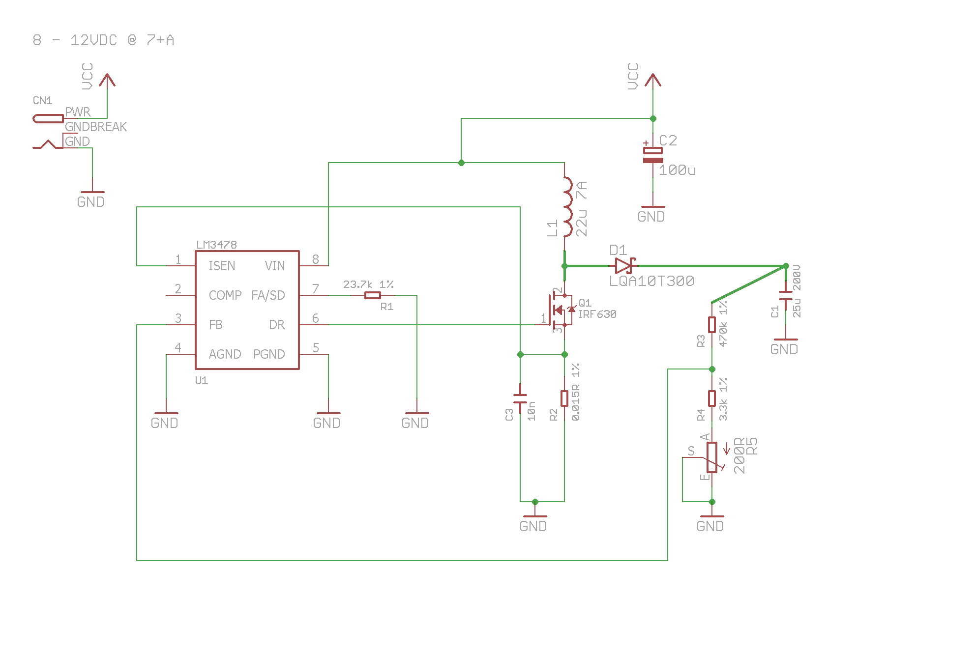
A boost converter design
05/12/2016 at 02:09 • 1 commentGoal: Design a boost converter that gives 170VDC at 0.15A from a 12VDC supply.
Adafruit has a nice boost converter calculator, assuming you're using the simple single-inductor version. To power my boost converter, I'd like to use a 12VDC wall adapter. I don't know, but suspect that the output voltage of the adapter will drop under load, so I'm just going to go ahead and specify a minimum input voltage of 8VDC. Min and max output voltage are 170VDC, output current is 0.15A, I'll specify an output ripple voltage of 2V, and a switching frequency of 150kHz. I hate low-frequency converters with their whining. Shut up already, converter!
This gives me a required inductance of at least 17.5uH capable of handling 4.25A. Also a duty cycle (switch on-time to total time) of 0.953. This rules out the popular MC36033, which has a max duty cycle of 0.857.
TL;DR: After the design procedure, here's what I ended up with:
![]()
Design procedure
The LM3478 datasheet provides a nice series of design procedures for various converter topologies. Here's the one for the boost converter:
Switching frequency
First, choose a switching frequency between 100kHz and 1MHz. I chose 150kHz because I wanted it to be above the minimum, but not so fast that all my components had to be super-fast.
Duty cycle
Next, compute the duty cycle, D. We got this from the Adafruit calculator, 0.953. Also convenient is the inverse duty cycle (proportion of off-time to total period), D' = 1 - D.
Note that the converter will adjust the duty cycle based on the output voltage and switch current, so this is only a value for calculation.
Minimum inductance
Compute the minimum inductance required. Again, this is from the Adafruit calculator, but here is the formula:
So with a maximum input voltage of 12V, and an output current of 0.15A, I get L > 12uH. Note that the Adafruit calculator (correctly, in my opinion) uses the lowest of two possible duty cycle based on the minimum input and output voltage, because this will result in the highest minimum inductance. In any case, I chose L = 22uH as a convenient value.
Maximum inductor current
Compute the maximum current flowing through the inductor. Again, Adafruit gives this as 4.25A, but the formula is:
And so I get a current of 4.92A. Again, Adafruit correctly is using the D based on the maximum input voltage, but I'm using a higher value for extra safety margin.
So based on the inductance and current, I can choose an inductor that can handle this current. Thus, I chose the Bourns 2105-H-RC, capable of 7A.
Frequency adjust resistor
The LM3478 uses this formula:
With my chosen frequency of 150kHz, I get 135.4k. I chose a 133k 1% resistor which slightly increase the frequency to 152kHz. I'll keep using 150kHz in the calculations as it doesn't matter much.
Current sense resistors
One of these is the resistor that goes between the switch and ground. This resistor protects the circuit against overload currents. We use the maximum inductor current from above, plus an additional 20% margin, to set the overload threshold:
And so I get a sense resistor of 0.014 ohms. I chose a standard resistor of 0.015 ohms (Stackpole BR3FB15L0). With that resistor, the current limit would be 5.52A, well within the maximum required 4.92A and the 7A spec for the inductor.
There is a second resistor which goes between the current sense pin of the converter and the current sense resistor. The datasheet recommends adding this resistor when the duty cycle is above 50% to prevent sub-harmonic oscillations (that is, oscillations lower than the switching frequency) caused by instability in the loop. No whiny converters!
We first calculate the maximum sense resistor for current mode loop stability (loop stability is always a good thing):
I get a maximum sense resistance of 0.004 ohms. Our chosen sense resistor is bigger than this by a factor of 3.75, so we need to add that second "slope compensation" resistor:
This yields 6.325k as the minimum slope compensation resistor.
The problem is that addition of this resistor modifies the current limit:
We must now change both the sense resistor and the slope compensation resistor so that the current limit is sane and the slope compensation resistor is above the minimum. Doing so (without going through the math) shows that it is not possible to pick a reasonable sense resistor while still maintaining a good current limit.
The cause of this is the insanely low maximum sense resistance from above. There are two ways to raise that maximum sense resistance: raise the frequency, or raise the inductance. Doing that also has a knock-on effect of lowering the inductor current. So this is really a good thing.
Thus, instead of a maximum sense resistance of 0.004 ohms, let's get this above 0.015 ohms so we can use the nice current sense resistor I found. This means raising the frequency (or the inductance) by at least a factor of 3.75. Since I kinda like the inductor I chose, let's raise the frequency from 150kHz to 600kHz and try again.
Our modified values with this frequency are:
The new current limit, of course, didn't change from before because we chose the same sense resistor. However, we now do not need a slope compensation resistor, and everyone is happy.
Diode selection
The diode has to be able to carry the maximum inductor current. It must also be able to withstand a reverse bias of the output voltage minus the input voltage. And, a Schottky diode is recommended for high speed. I chose the Power Integrations LQA10T300 diode, which has a max reverse bias of 300V and a current limit of 10A. The datasheet also says it is capable of 1A/ns, so presumably it can turn off a current of 3.62A in 3.62ns.
MOSFET selection
Look at the frequency, and then the duty cycle. The off-time is 0.047 / 600kHz = 78ns.
The LM3478 datasheet, however, kind of gives up on being able to choose a MOSFET. Other than being able to withstand the output voltage at the drain (max Vds) and the inductor current (max Id) and being able to turn the MOSFET on in the first place (threshold Vgs < 7.2V), the only real recommendations are for a low on-resistance and for it to be "fast". Clearly such a switch has to shut off well before 78ns.
I chose the STMicro IRF630 MOSFET. It can withstand at least 200V to the drain, and has a gate threshold of at most 4V. It can handle currents up to 9A, and has an on-resistance of 0.35 ohms.
Can this thing switch fast enough? Nobody will know unless we try it. If not, there are chips specifically designed to drive MOSFET gates at higher currents to force them on and off quickly.
Output capacitor selection
You want something big with low ESR. I chose the Panasonic EZP-E50256LTA, 25uF, 500V, ESR of 8.8 mohm.
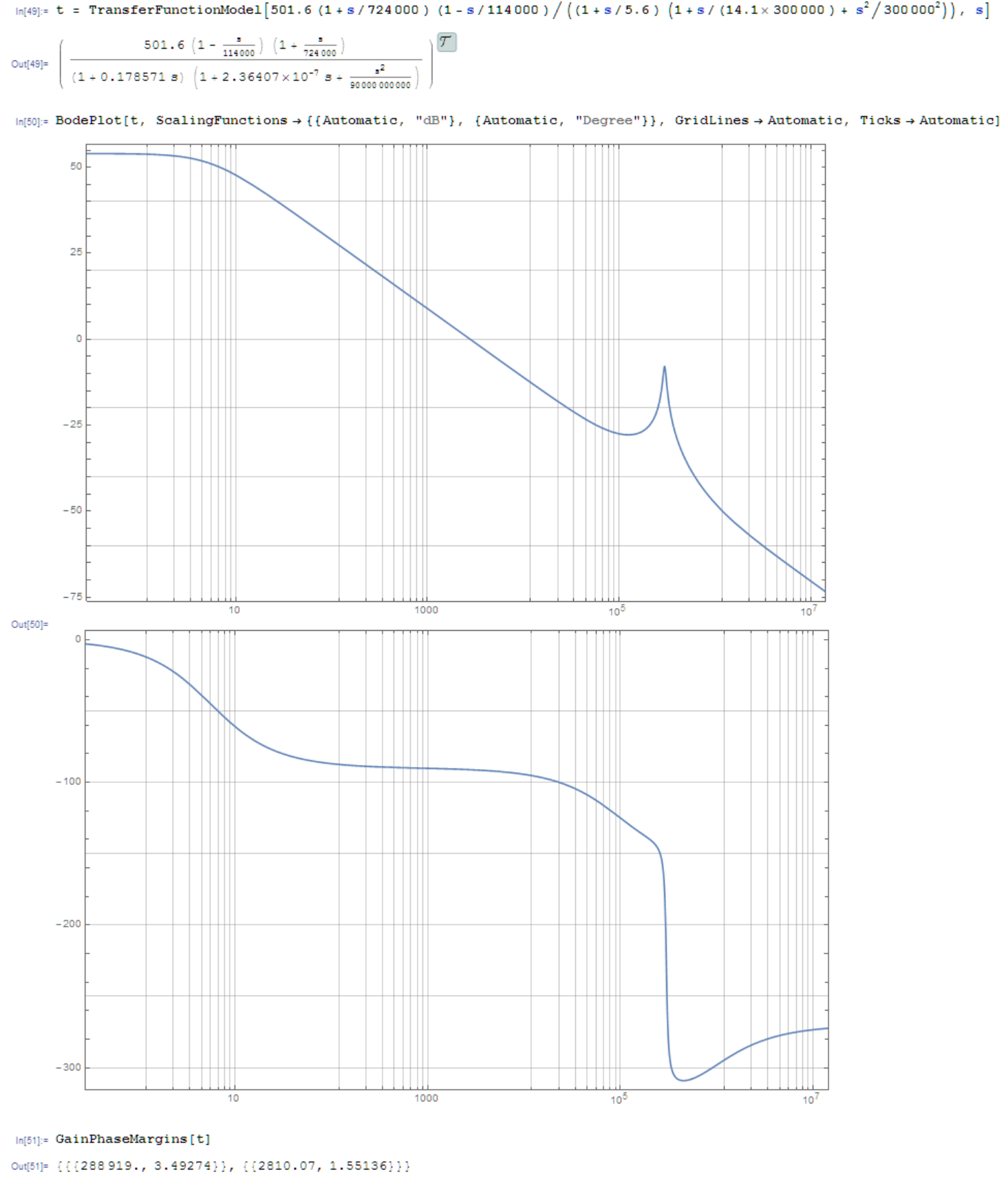
Compensation
There's a COMP pin on the converter where you put a resistor and capacitor in series. They are there to add stability to the converter. The converter is a feedback loop, and such feedback loops need to be stable, otherwise your power supply might fail at certain frequencies. We will be following Application Note 1286, Compensation for the LM3478 Boost Converter. If you don't know anything about control theory, you probably want to skip this section. The problem is, without knowing control theory, it will be difficult to select the compensation components. Maybe start with this list of videos?
So, let's take a look at the application note to see what the transfer function looks like without this compensation.
We see that there are two zeros, one pole, and one complex pole:
The first zero, z1, is caused by the output capacitor with its ESR. The second zero, z2, is caused by the inductor and the load on the power supply. The pole is caused by the output capacitor with the load, and the complex pole is caused by the switching action.
Let's locate the zeros:
From this, we have (I'll show frequencies in Hz rather than rad/s):
Note that the second zero is a right-hand plane zero. This means that in gain it acts like a zero, but in phase it acts like a pole.
Next, we locate the simple pole as follows:
And so:
And now for the complex pole. We need to find Q, which is the damping factor. If Q were infinite, the thing would vibrate itself to pieces and catch fire at half the switching frequency. But, of course, this will not be the case.
Remembering that VSL = 92mV from the datasheet, we have:
And, of course, this pole is located at half the switching frequency:
Now that we have our pole and zero frequencies, we need to know what the DC gain is. It is:
where VFB is the feedback threshold voltage, 1.26V from the datasheet. So, we have:
OK, at this point I could draw a Bode plot by hand, but I have Mathematica, so I'll just leave this here:
![]()
The top plot is gain in dB vs frequency in Hz, and the bottom is phase shift in degrees vs frequency in Hz. You can see the resonance at half the switching frequency.
The phase margin is 180 degrees plus the phase at which the gain is unity (0 dB). We can see that unity gain occurs at 2.81 kHz and the phase margin there is 1.551 radians (88.9 degrees). This is fine, since the application note states we want a phase margin between 30 and 100 degrees.
The gain margin is minus the gain at which the phase is -180 degrees. Here we see the gain margin is 3.5 = 10.9 dB at 289 kHz.
These margins are important because the poles and zeros shift with varying load and input voltage, and without these margins your circuit could go unstable. However, the margins cannot be too great otherwise the system doesn't react quickly to changes.
The datasheet doesn't state this, but ideally the gain margin should be somewhere between 6 and 12 dB. And indeed it is.
So, in fact, this converter with the components so far needs no compensation network, and we can leave the COMP pin unconnected.
Conclusion
Well actually there is no conclusion until I actually get the parts in to build this thing. Will it work? We'll find out in the next project log.
-
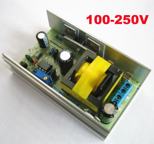
Power
05/11/2016 at 03:50 • 3 commentsIn the previous log I was pretty happy with my transformer power supply. Then I realized that at full load the voltage out dropped too much. I would like to keep the output at 170VDC.
So, I wanted to find a regulated high-voltage power supply. First I designed a boost converter that takes 12VDC in and yields 170VDC out. It might work, I just need the parts to come in. The problem with such high voltage ratios is that they lead to a slow charge time for the inductor, followed by a very fast drain into the output capacitor. So it requires high-quality high-speed low-ESR parts.
Apparently you can use a transformer instead of an inductor, but I hate transformers because I don't know how to wind my own (I really should learn, though), and almost inevitably the specs I need aren't anywhere to be found.
In the meantime, I found a Chinese manufacturer on ebay that makes 12VDC in to 100-250VDC out, 70W open-frame supplies. It looks like a plain old boost converter with a big transformer. The chip, predictably, has its top dremeled off so that we can't see what it is, but of course it's going to be an 8-pin dc/dc converter chip, so it doesn't really matter what it is.
![]()
I bought two. One for testing and one for tearing apart to reverse engineer and post here. If it works, great. If it doesn't, oh well, it was only USD 12.50.
The power supply is arriving via ePacket from China. This is basically a free shipping thing that the US and China has going. But it takes a while, like up to three weeks. I've had better shipping times, though, since I'm on the west coast of the US. So hopefully I'll have this soon.
-
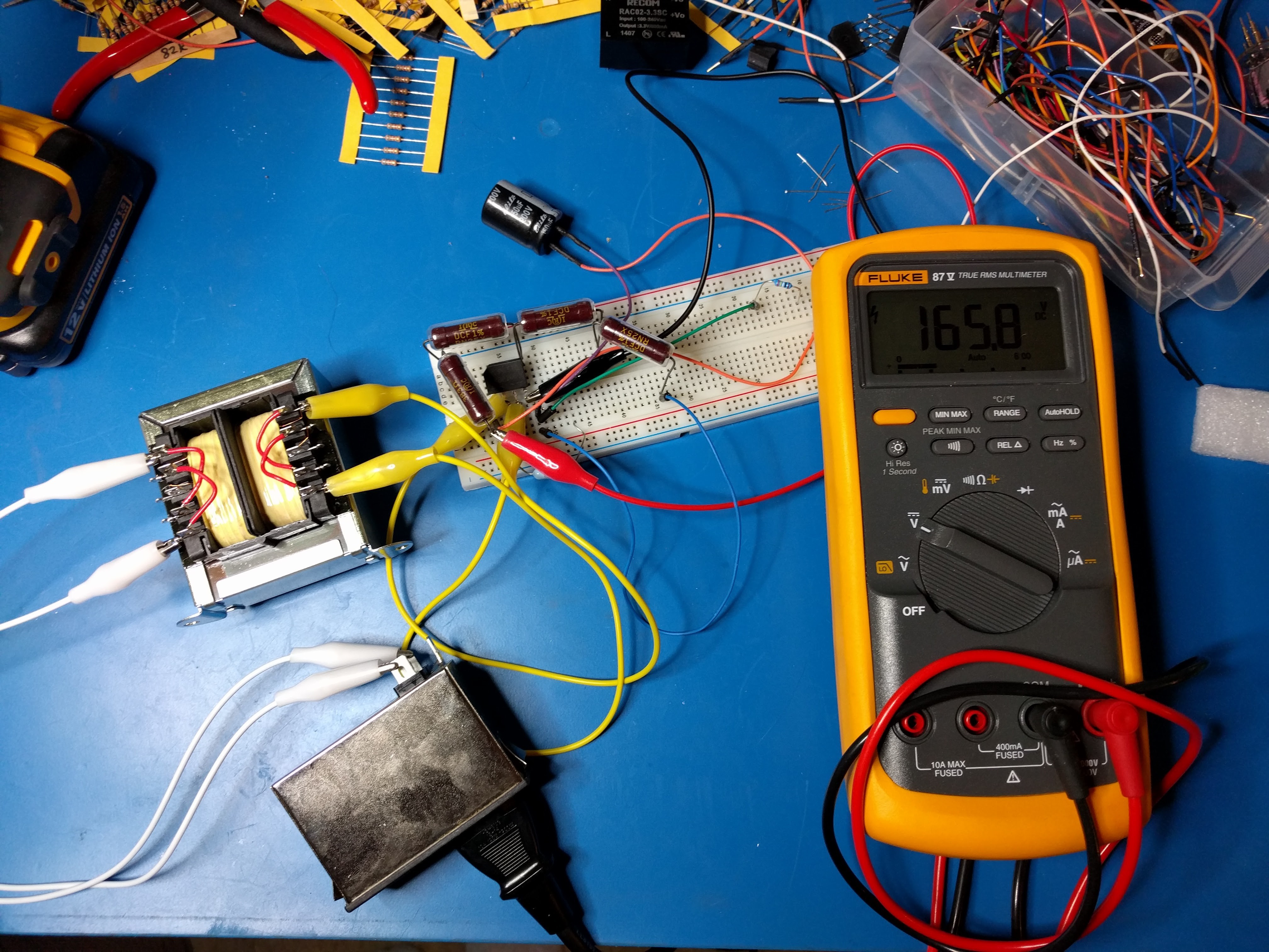
Transformer part 4
05/02/2016 at 03:28 • 0 commentsSuccess! A 1:1 transformer (Triad Magnetics VPS230-190, a 43W transformer) worked much better than a step-down followed by a step-up transformer.
![]()
I hit 166VDC at 110mA. I did some more science to get power losses.
![]()
A few interesting things. First, the 1:1 transformer isn't quite 1:1. In fact, turning the transformer around got me only 127VDC, so I have to keep the orientation correct. Second, there is between 3.6W and 4W being lost in the transformer. Finally, the power lost in the rectifier/capacitor is 1W at the low end, and 6W at the high end.
The inlet I used (Delta Electronics 06AK2D) is an EMI filter, switched and fused for 6A.
With the power circuitry decided upon, I can finally get to the business of testing the Nixie driver board.
-
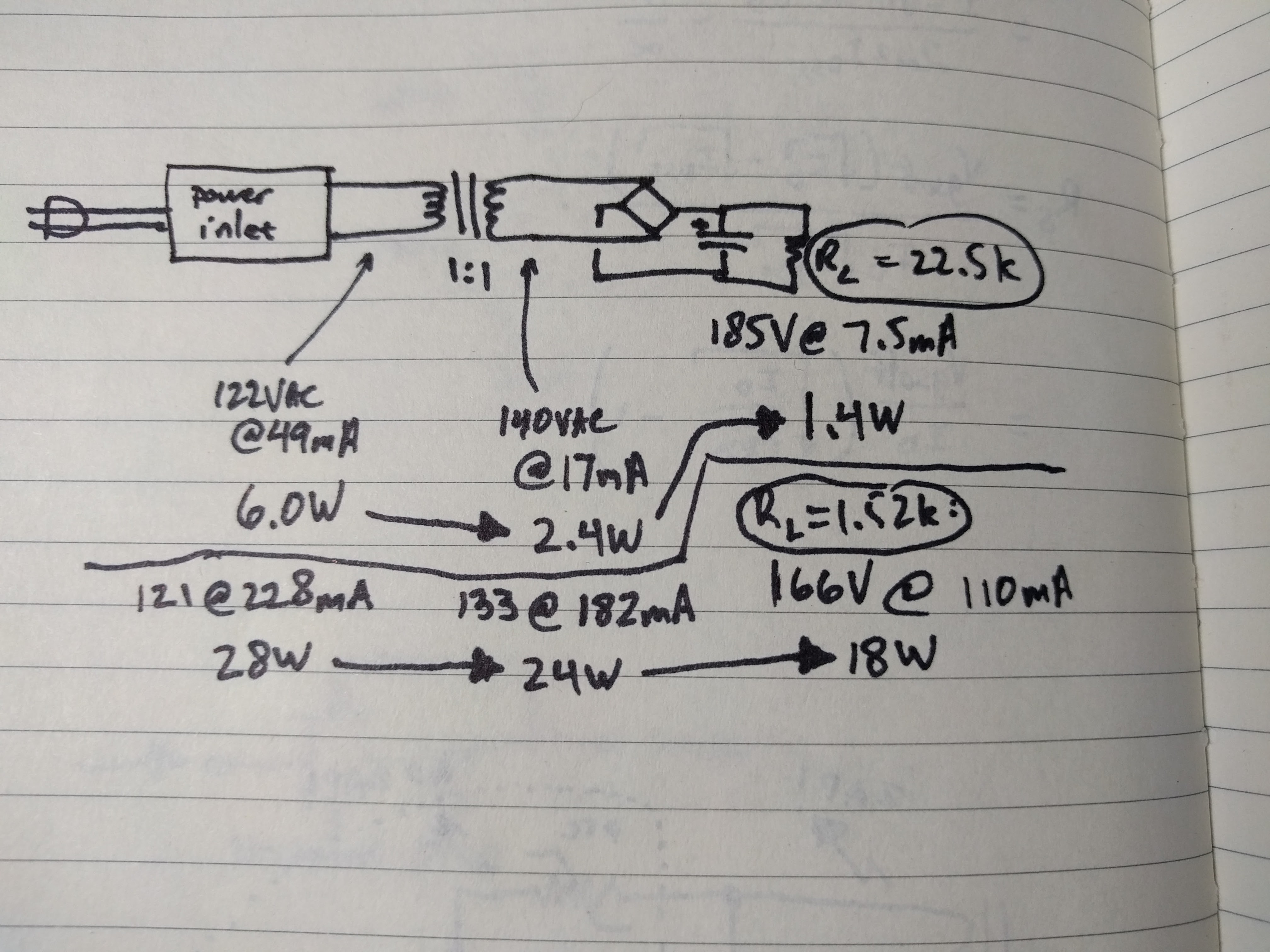
Transformer part 3
05/01/2016 at 05:11 • 0 commentsI feel like I've taken a crazy pill. I measured the voltage and current at four points in the circuit. First, at the wall. Next, between the two transformers. Then, after the two transformers (the input to the bridge). Finally, the DC output across 22.5k.
At the wall: 150mA AC @ 122VAC (18.3W RMS power)
Between the transformers: 460mA AC @ 15.6VAC (7.2W RMS power)
At the bridge: 13.1mA AC @ 115VAC (1.5W RMS power)
At the load: 6.2 mA DC @ 154 VDC (1.0W)
That's an immense power loss. The first transformer is losing 11.1W and the second transformer is losing 5.7 watts! And then the bridge (and maybe the capacitor) is losing us another 0.5 watt. No wonder this thing is not performing the way I expect, especially when I load it down with more current and the voltage output drops. Maybe these transformers are just crap?
I loaded the output down with 1.52k (four resistors in series, each 25W) and measured an output voltage of merely 118VDC. That's terrible and that's just about halfway to what I really need.
The reason that I chose this step-down step-up configuration was for safety, so that you'd never have to plug in something lethal. The lethality would come after the step-up transformer.
On the other hand, we plug in 120VAC appliances to the wall all the time. Perhaps I should start thinking of just using a 1:1 isolation transformer and live with the fact that both sides of the transformer are now lethal.
RPN Nixie Calculator
A programmable RPN calculator using way too many Nixie tubes