Close
0%
0%

FPGATED

Reimplement the TED chip of Commodore 264 series in FPGA

Similar projects worth following
A cycle exact FPGA core for the MOS 7360/8360 TED chip written in verilog.
The final goal is to have an fpga core that could be used as a drop in replacement for the MOS 8360 chip which is the heart of the Commodore 264 series 8 bit computers, namely the Commodore 16, Commodore Plus 4 and Commodore 116. This core can be the basis of a complete C16 or Plus 4 SoC implementation.

The idea of the project came when my 30 years old Commodore Plus 4 has suddenly died and I suspected that TED was the main cause. After an extensive troubleshooting it turned to be that the 8551 ACIA chip was the guilty one and I have fixed it, however by that time this project has been born in my head. I have checked the internet and was surprised that no one has created a TED FPGA core before.

Although there are some TED documents available on the internet, they are incomplete, not precise and do not fully describe the inner secrets of the chip. There is no point in creating a chip which is not cycle exact, doesn't emulate TED scan lines and events properly. An extensive research started on the hardware using own written test codes, logic analyzer, oscilloscope and source code analysis of Plus 4 emulators. I quickly realized that due to the inner multiplexed architecture of TED certain events are initiated at the specified time (described in 7360R0 preliminary data sheet) however they happen later in time after 1-2 single clock cycles. This behavior was emulated in certain emulators like Plus4emu, which made the emulator code much more difficult to understand.

Two years of analyzing the hardware, documents and code writing has led me to a working TED chip which is capable of running most of the programs and demos the same way as the original hardware. The project is not finished though, I am planning to refine it further and make it available to everyone.

The code is written in verilog language and uses Gadget Factory's Papilio One 500k developer board. This board has a Xilinx Spartan 3E 500k FPGA which is more than enough for implementing a whole Commodore computer except its main memory. The FPGA has only about 40Kbyte RAM which is not enough for a 64Kbyte computer especially if we think of the 16K Kernal and Basic ROMs. The TED core module doesn't use any Xilinx specific HW blocks or macros so it is very easy to reuse on other Vendor's FPGAs. Later on I have continued the development on the more advanced Papilio Pro board with Spartan6A FPGA and onboard sdram. Although I wanted to implement the TED chip , it was clear that I need to implement other supporting components (CPU, ROM, keyboard matrix) to test the chip on the FPGA board. As several 6502 CPU FPGA codes exists I did not want to reinvent the wheel and decided to use a publicly available one which has illegal opcode implementation also. I have chosen Peter Wendrich's 6502 vhdl code from the fpga64 project. Peter has confirmed via email that I can use the CPU part of his code for my FPGATED project and include its source in FPGATED sources.

Papilio TEDwing

First step of the project was to create the hardware developer environment, which means building a suitable wing board for the Papilio One FPGA board. Gadget Factory has already created an Arcade Megawing however it lacks the memory part which is crucial from the TED system's point of view. It was however a good starting point for the TEDwing design. These were the main design criteria for the Papilio TEDwing:

  • 12 bit VGA/RGBS output
  • 2x 4464 DRAMs
  • IEC serial bus connector
  • PS2 keyboard connector
  • Stereo audio out with low pass filter
  • RS232 serial output
  • Reset button
  • Jumper to configure VGA or RGBS mode

The board schematic was inspired by the following other designs

  • VGA, audio and PS2 part from Papilio Arcade Megawing
  • IEC serial bus from SD2IEC design
  • DRAM from Quickswitch QS3 voltage level translation application note AN-11A
  • RS232 from MAX232 application notes

I have used Eagle 6.2 to create board schematic and layout. Size of the board fits to the limitation of Eagle free edition. All traces of the PCB was manually routed by me then sent for manufacturing. SMD soldering of components were done by me without hot air gun.

The above mentioned features fully utilize free Papilio I/O ports so there is no space left for joystick connections or user port. This is a small drawback however the original goal was...

Read more »

FPGATED v1.3.zip

Improved TED core (v1.3). DMA delay is fixed and challenging games like Alpharay, Pets Rescue work now correctly. Some additional output signals defined for ted module in order to connect chroma/luma generator and real C16/Plus4 bus.

x-zip-compressed - 2.19 MB - 01/13/2021 at 21:27

Download

FPGATED v1.2.zip

Check out the latest bug fixed FPGATED core (ted.v) and a modified C16 system (c16.v). Compatibility is highly increased thus FLI/HFLI pictures are shown correctly!

x-zip-compressed - 2.19 MB - 10/04/2019 at 15:27

Download

FPGATED v1.1.zip

Joystick emulation added on PS2 keyboard numeric keypad. c16.v and c16_keymatrix.v modules are modified to implement joystick emulation. F11 selects between joy0 or joy1, numeric keypad directions are joystick directions, numeric 0 key is the fire button.

Zip Archive - 2.00 MB - 08/23/2016 at 20:05

Download

FPGATED v1.0.1.zip

Source files of FPGATED v1.0.1 Minor bug fix on c16.v

Zip Archive - 2.00 MB - 08/08/2016 at 21:52

Download

Papilio TED wing.zip

Eagle schematic and board files for Papilio TED wing

Zip Archive - 103.42 kB - 05/05/2016 at 09:24

Download

  • 1 × Papilio One 500K developer board Gadget Factory's Open Source FPGA development board based on the Xilinx Spartan 3E FPGA
  • 1 × Papilio TED wing An own designed and built wing for the Papilio One 500K board
  • 1 × VGA to Scart cable An own built RGBS video cable (same as Minimig scart cable)
  • 1 × Papilio Pro FPGA development board Gadget Factory's Open Source FPGA development board based on the Xilinx Spartan 6 FPGA

  • FPGATED HW Version 3.0

    István Hegedűs02/22/2024 at 14:05 2 comments

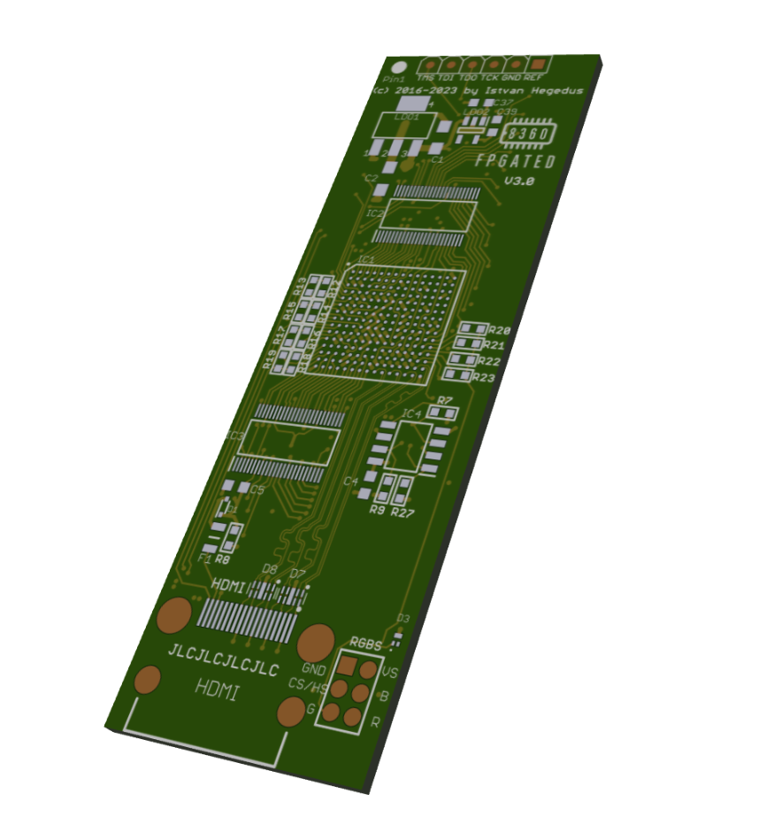
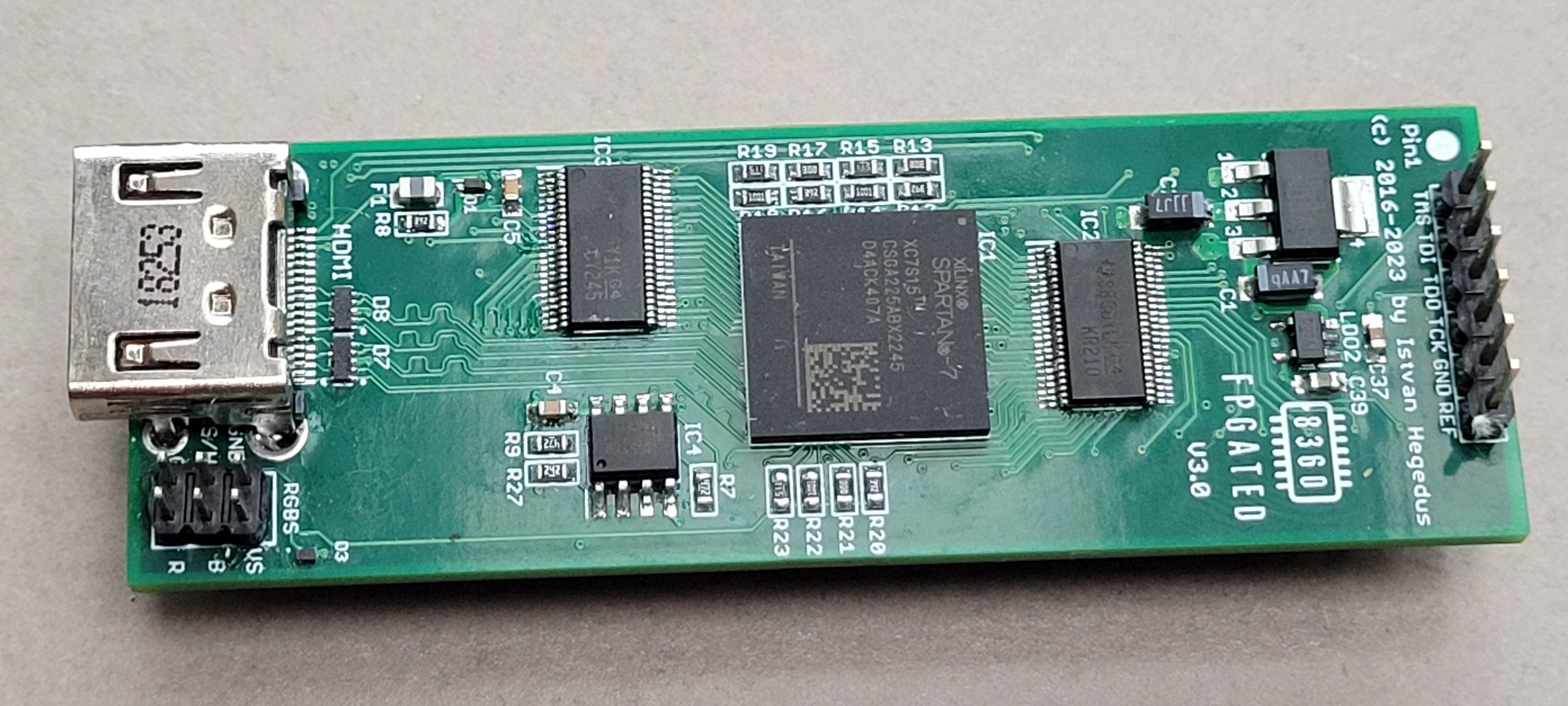
    As we have reached the end of chip shortage period I am glad to announce that I have finally finished the HW design and prototype testing of FPGATED. The last years were challenging, especially with Xilinx AMD acquisition and the production stop of Spartan 6 FPGAs. My original design was based on the Spartan 6 FPGA and even though I had two prototypes working, I had to come up with a successor that can be produced for the audience. An obvious path was to use the Xilinx Spartan 7 but as much as it was easy to modify the internal code it was challenging to redesign the PCB for Spartan 7. Hardware version 3.0 is the result of this redesign and I can proudly say that it works flawlessly! 

    FPGATED HW version 3.0 has the following features:

    - Xilinx Spartan 7 XC7S15CSGA225 FPGA

    - Most resource utilizations are below 50% thus plenthy of room to add new features!

    - Original analog Chroma and Luma output to get picture via RF modulator

    - RGB header onboard which is software programmable between 15KHz SRGB and 31KHz VGA output

    - HDMI connector with digital output with 720x576/50Hz or 720x480/60Hz output

    - Digital audio output on HDMI connector, so you can hook up the C16 or Plus4 to a modern flat TV

    - Software switchable scanline effect on HDMI and VGA outputs

    - 4 software selectable color translation tables for HDMI, VGA or SRGB outputs (FPGATED Caclulated, Plus4emu, YAPE, Custom) 

    - 1 software programmable custom color table (out of the 4 tables) to be able to adjust RGB colors (CVBS is not affected)

    - theoretically firmware upgradeable from Plus 4 side (but 1 floppy is not enough for firmware)

    - ESD protection on HDMI connector and VGA header

    What is next?

    Calculating HW cost and seeking for HW production possibilities. My plan is to start with batches and sell them via e.g. Amibay. Also I am going to write a software to modify configuration registers and the custom color table. The configuration is saveable to flash!

    Further development is ongoing to add a SID chip implementation and improve TED core compatibility,

    The VGA/SRGB header requires a special cable that will be sold separately (or can be built by anyone).

  • Hardware revision 2.0

    István Hegedűs05/14/2022 at 20:10 2 comments

    Dear followers,

    I know it has been a long time now I last posted update on this project, however I can assure everyone that this project is not dead. As everyone knows there is a global chip shortage which impacts the commercial release of FPGATED. Unfortunately at the moment the prices and delivery times of FPGAs are not making this replacement a cost effective solution.

    In the meantime I have redesigned it to v2 HW version using a smaller BGA chip and a HDMI connector. Also the bus switch I have used is End  of Sale so I had to redesign it using TI chip for voltage translation.

    At the moment I am in the challenge of hand soldering it and then test the HDMI output. When ready I will post more pictures and video about it. 

    After that the production can start and I want to make it available. In order to make it even more cost effective I am planning to shift to Spartan7 FPGA in v3 version (which I am currently unavailable to procure even for prototyping).

    Please be patient.

  • FPGATED prototype is working in a C16!

    István Hegedűs01/14/2021 at 21:06 3 comments

    Hi,

    Heading into 2021 here is an awesome news for those who are waiting this moment for 4 years now! I have managed to build the first prototype of the FPGATED IC which is a direct drop-in replacement of MOS 8360R2 IC. 

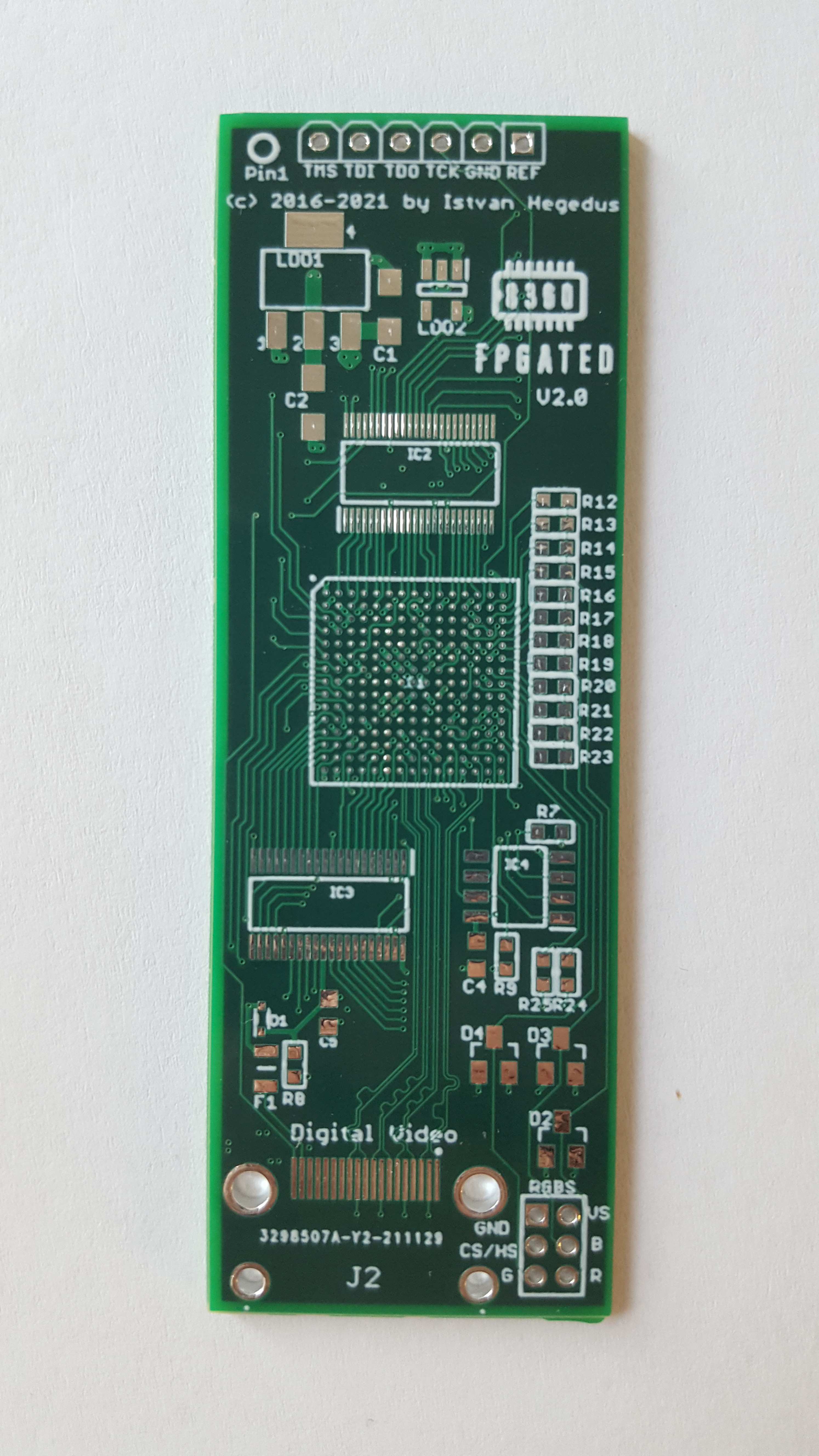
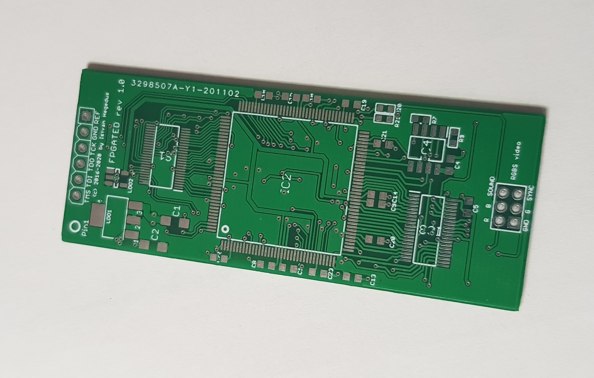
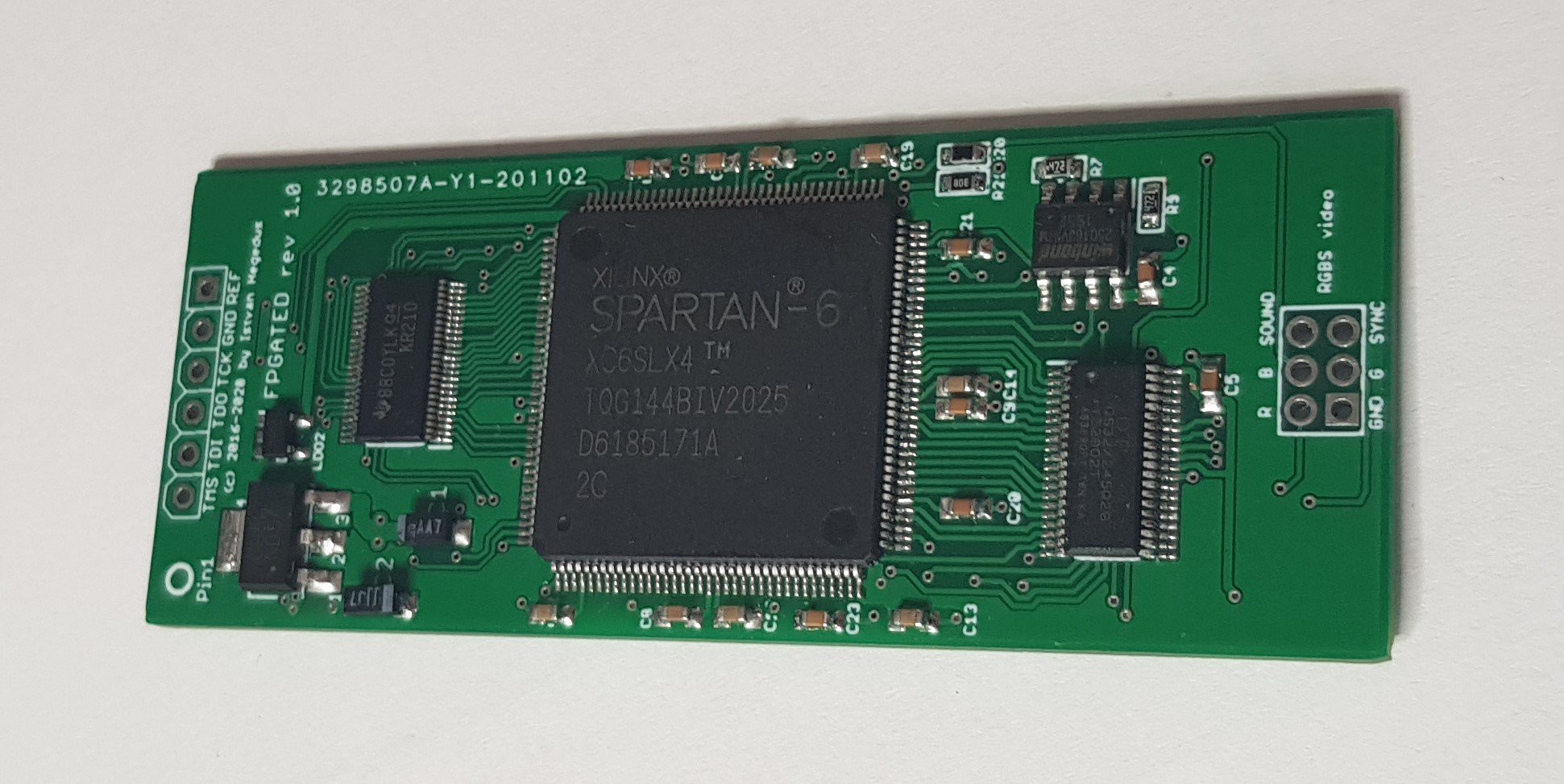
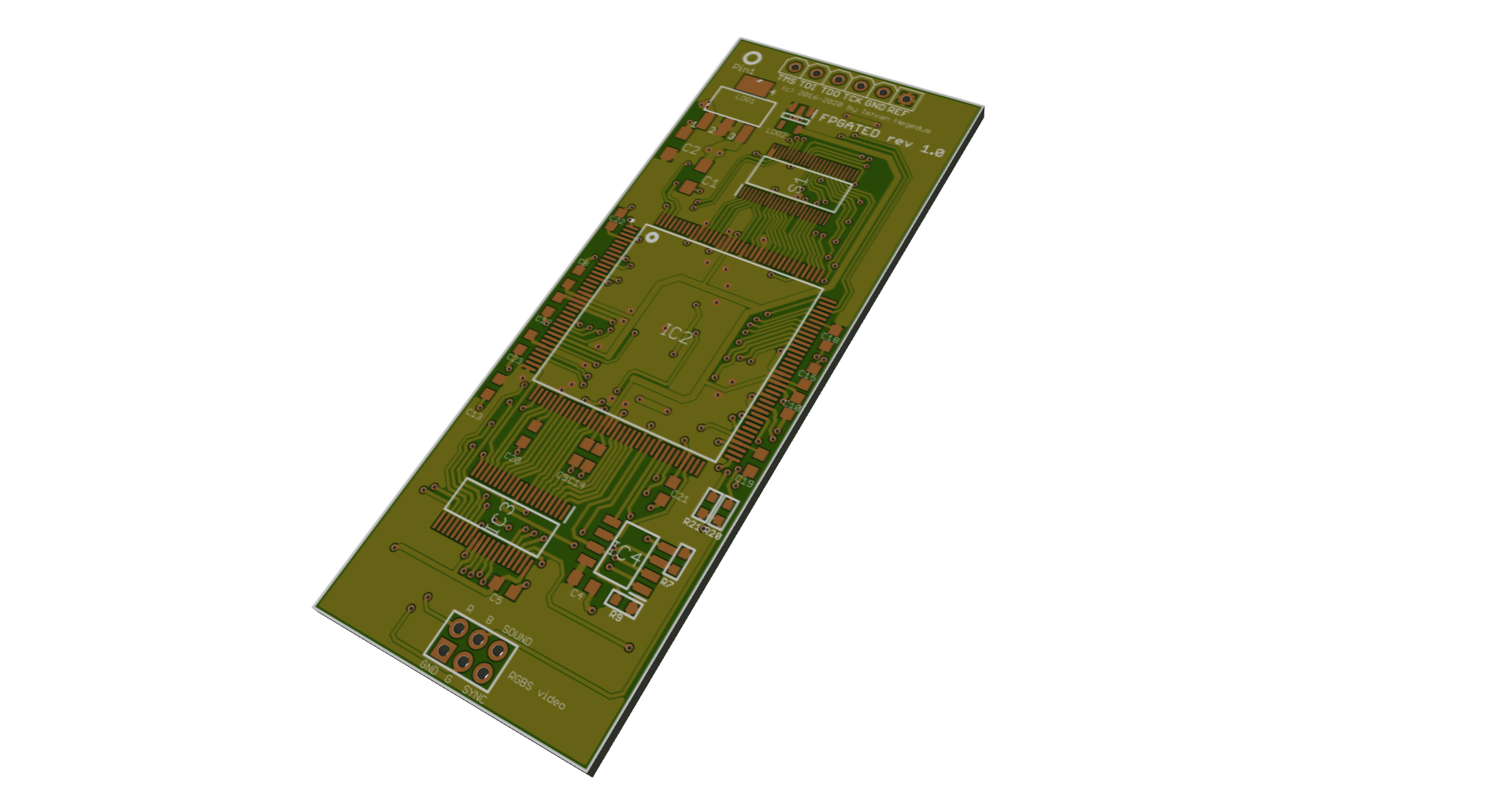
    Here you can see how the empty and populated PCBs look like on the top.

    FPGATED PCB
    RAW PCB Top
    FPGATED populated board
    FPGATED top

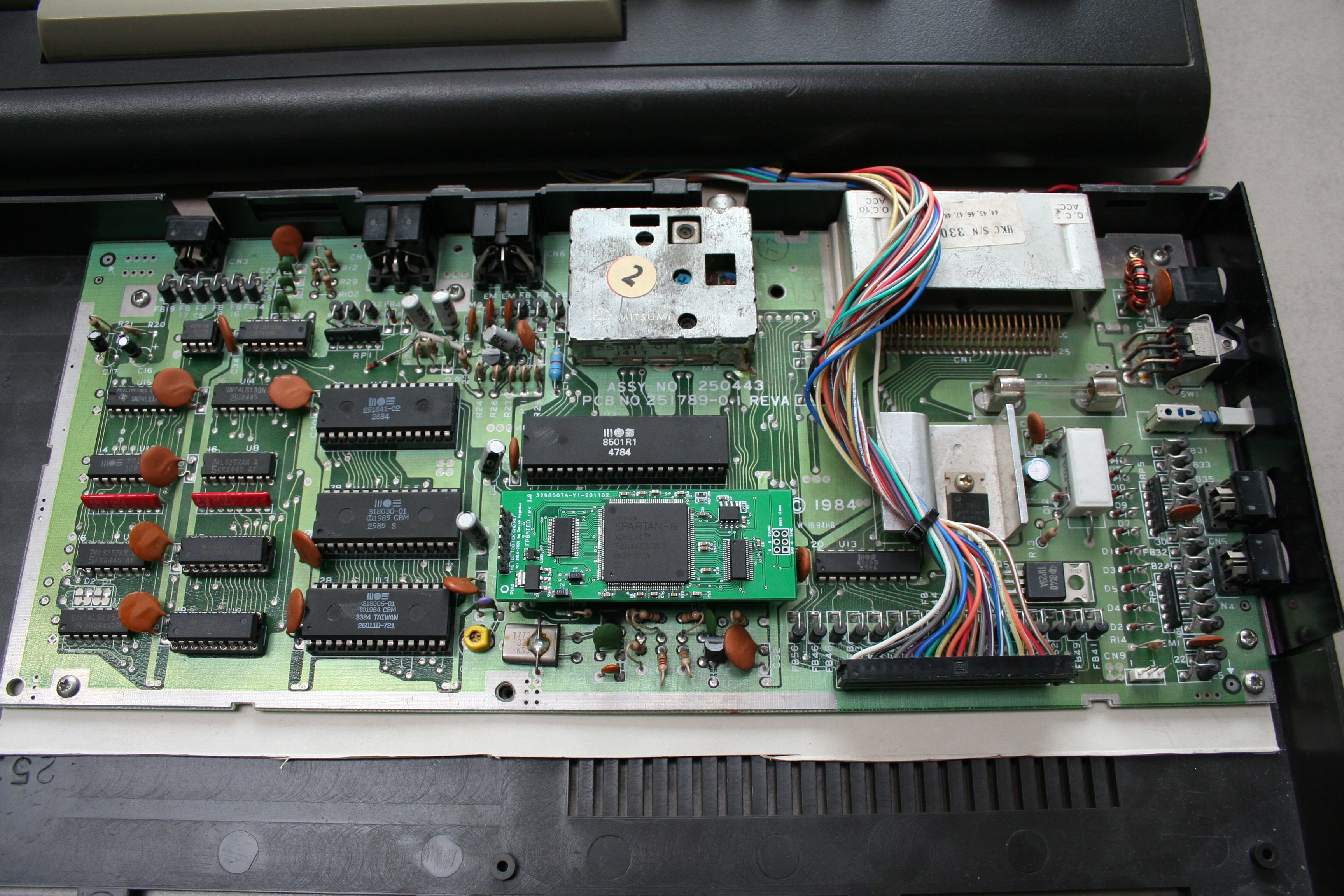
    The size of PCB just fits into a Plus4's TED shielding and fits easily in a C16. Although I have tested it in both machines further testing is done using the C16 because it has more space and it is easier to load the firmware via the JTAG connector. 

    The board has two level shifters for those signals which need it. Outputs from TED's point of view don't need level shifting because they are LVTTL compatible, only bidirectional or input signals are translated. Interestingly the motherboard's clock signal stays  under 3.3v (see PLus4 or C16 schematics which gives explanation) so it is directly connected to the FPGA. Two cascaded LDOs create 3.3v and 1.2v supply voltages from 5v. As the 2nd LDO is supplied from 3.3v the heat dissipation is minimal and the component stays cool during operation. 

    Inside a C16
    It fits easily Inside a C16

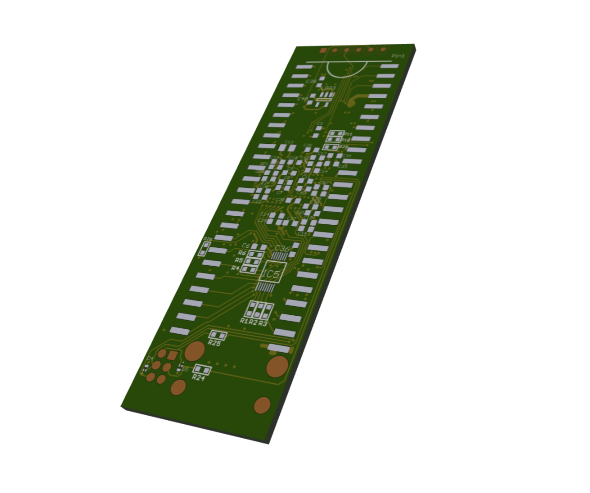
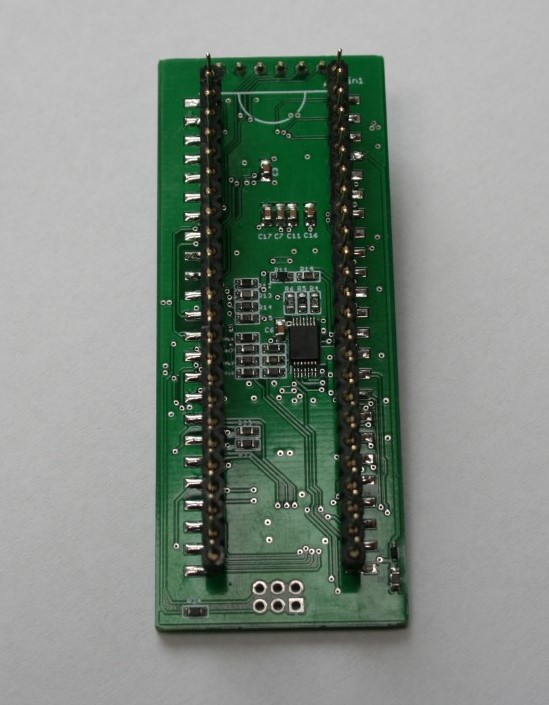
    The backside of the PCB has an SMD IC header which together with the FPGA are the most expensive parts of the whole device. To keep cost as low as possible a Xilinx Spartan6 LX4 FPGA is used which still have empty space left inside for further improvements, but it can be replaced by an LX9 if needed (of course not by users).  As the SMD IC header has still not yet arrived I had to create a temporary solution using straight through hole IC headers. As these are for through hole applications, the shorter pins which are normally soldered inside the PCB holes are now soldered to the smd pads. Benting them would break them so this was the easiest way to test the device without the final header. I was surprised how solid it is when soldered! The only drawback is that the device is now too high when inserted to the TED socket (which is not an issue in a C16, but might be problem in a Plus4). But hey this is just a prototype!

    FPGATED backside
    Back side of the PCB

    The components I have soldered with my hands (takes time but not that difficult when you have a microscope). 

    I was afraid that during power up the configuration of FPGA will not finish by the time the reset cycle finsihes (about 500ms), so in the design I have taken this into account. In order to speed up the configuration time during power on, the onboard SPI flash has a quad connection and the bitstream utilizes it with a 10Mhz configuration clock. Needless to say that it works perfectly! 

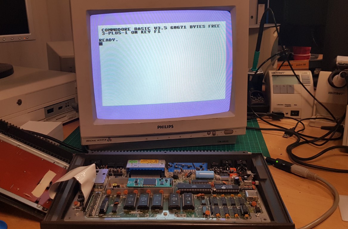
    I have programmed it via iMPACT and turned on the Plus4 with high hopes (yes, first I have tried it in a Plus4).

    FPGATED in a Plus4
    First power on in a Plus4

    It works! Thanks to the careful design, individual part testing it works perfectly! The image is generated via the composite video out and RF modulator (I was surprised how much better the Plus4's RF modulator is compared to the C16. It gave much sharper and clearer picture). I have adjusted the color phases to be as close to the original as possible, I have even done measurements on real TED via oscilloscope and calculated phase angles from time differences between burst and color signals. 

    Since the first power on I have used it a lot and tested serveral games, demos. I have fixed DMA delay in TED core (see release latest source code) and now everything I tested so far works fine!

    So what are next steps?

    I am waiting for the smd IC pin headers and can build some more units (I have components for about 10 now), The PCB has an SRGB header also which I have not yet tested. What I regret is that this header does not have hsync/vsync just csync. So if I want to implement scandoubler I need to redesign this part.

    • I am going to design a 4 layers PCB for the cheaper and smaller BGA Spartan6 using through hole pin header (v2). ...
    Read more »

  • FPGATED hardware rev 1.0

    István Hegedűs11/04/2020 at 21:23 2 comments

    FPGATED hardware prototype is now in the finish!

    The schematic and board layout was finalized, ready for PCB manufacturing.

    This is hardware revision 1.0 using a TQFP144 Spartan6 FPGA. It is only a 2 layers PCB so most probably rev 1.0 is not the final production one. The main goal is to test all functionality in a C16 or Plus4 and then shrink it even further. 

    The production version will use a smaller BGA package FPGA with 4 layers PCB and cheaper IC socket connector. This one features an SMT mounting socket connector at the back in order make space for the TQFP144 on the top. Good news is that I have managed to route the RGBS signals to a small 2x6 connector on the top, so besides composite, RGB video signal will be available too.

    I am now sourcing components but 2 items on the list has a bit longer lead times than I expected, so expect it running in Q1 2021!

    Stay tuned!

  • TED analog part implemented

    István Hegedűs06/12/2020 at 15:55 0 comments

    I am glad to report that the analog picture generation part of the drop-in TED replacement is ready!

    The luminance signal is implemented with a look up table and a smart external circuit which is not a DAC so it generates perfect voltage levels for the various luminance signals (I don't want to release the circuit details at this point).

    The chrominance signal was easier than I thought, however the DDS phase accumulator I had to increase to 24 bits because it turned out that the PAL standard requires very precise 4.433618 MHz frequency. Unfortunately I cannot test NTSC as I don't have an NTSC monitor but I am implementing that part too!  I will leave that later for test users from US region.

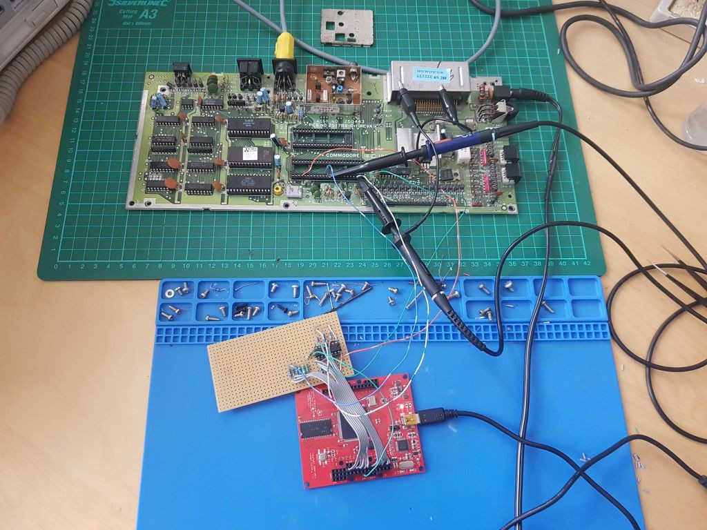
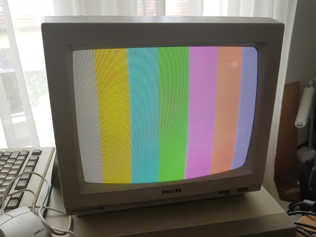
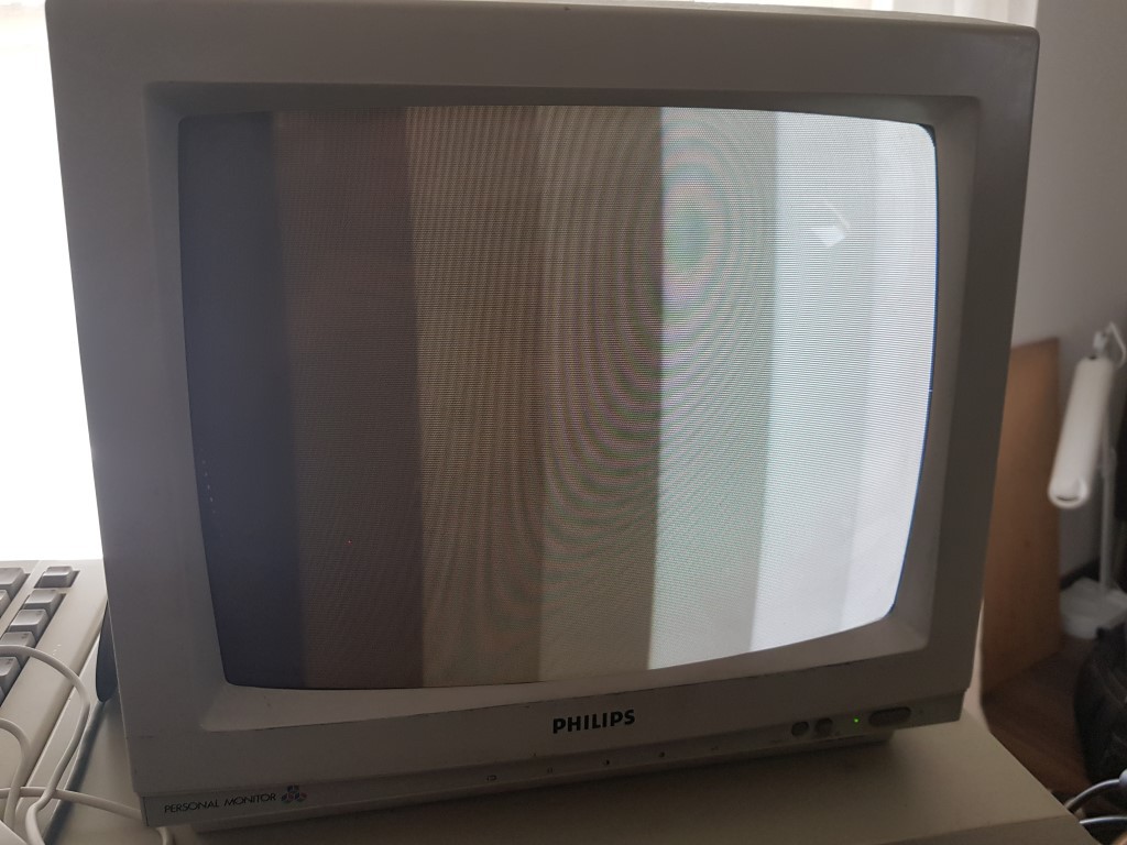
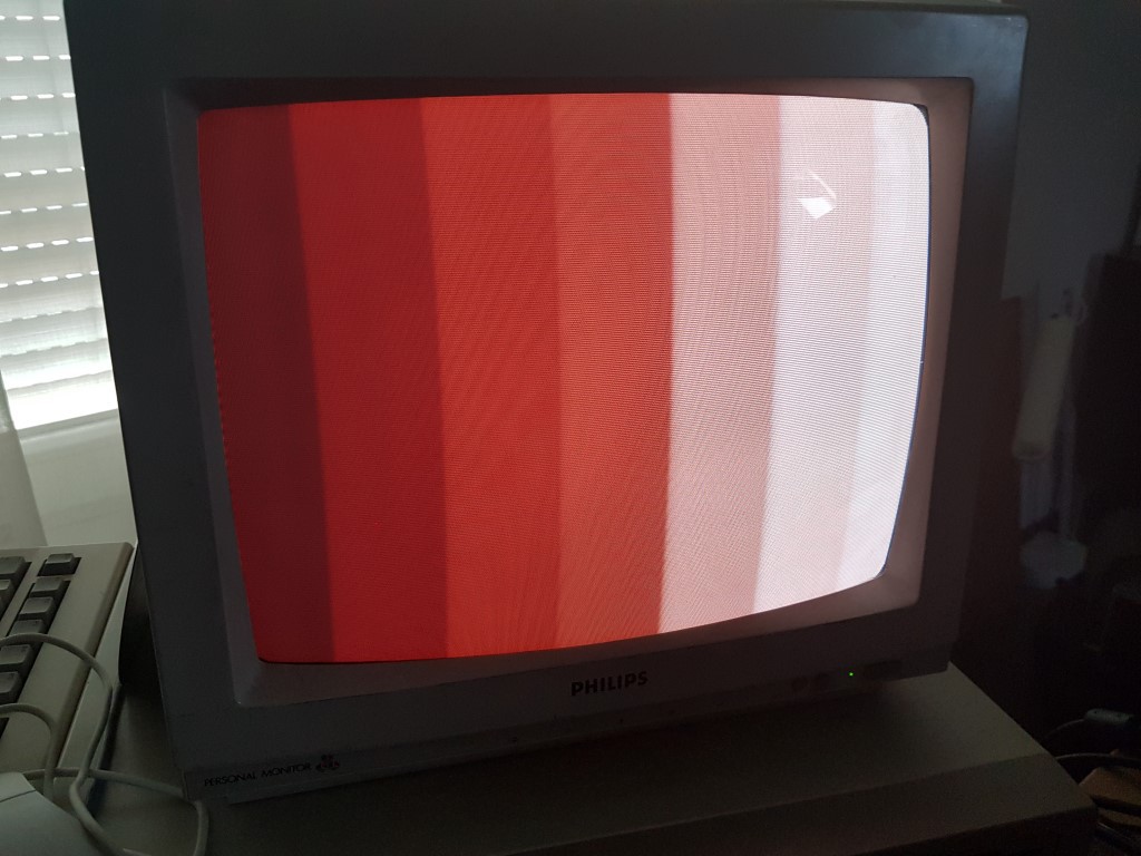
    To test the result I have created a PAL test screen top module which generates SMTPE bars and/or different color bars that I can change in code. The FPGA board I have hooked up to a C16 motherboard via TED chip socket's Sync and Color pins in order to see the real composite output on my monitor. The result pictures speak for themselves.

    This is my testbench using a Papilio Pro board and some analog components on the test board.

     SMTPE color bars generated via the FPGA and C16 RF modulator. 

    (those moisters are visible only on the photo, but in real life they are not visible)

    Testing luminance levels with white color (grayscale).

    Same luminance test with red color bars.

    Next step is to start to design the PCB! It will take some time as I have never designed a 4 layers PCB with BGA chip on it. Current FPGA choice is Spartan 6 LX4 or LX9. My goal is to keep cost as low as possible to create a competitive chip in price.

  • Drop in replacement progress

    István Hegedűs05/13/2020 at 08:38 0 comments

    Update on FPGATED drop in IC replacement.

    The drop-in TED replacement's biggest challenges are

    - the analogous part of the IC (Luma and Chroma generator)

    - component sizes on the PCB to fit the small space in the Plus4's metal cage (C16 is not an issue)

    Over the last months I have been investigating these and created some proof of concepts. Unfortunately I had to rule out the using of an external video signal generator like the AD724/AD725 IC because the RF modulator of Plus4 and C16 delays the chroma signal too much (about 100ns) which requires a luma delay circuit to get them in phase. Delaying an analogous signal is much more difficult than delaying digital one thus I have turned to a different approach.

    The luma signal can be created relatively easily in the FPGA using LUT for the luma values and requires just a few external components (resistors) before connecting to the RF modulator. Here the only challenge is the external voltage levels which should be between 0 - 4.8v. This part has been solved.

    The chroma signal requires DDS to create the sine wave and modulate its phase. This is not too difficult either, however it requires some careful planning in order to have an optimal design and not to over complicate things. Some of the questions are, how large should be the phase accumulator and the DAC resolution? Do we need a high precision DAC? What should be the internal clock frequency for the DDS keeping in mind that we need to implement PAL and NTSC both? I have done simulations in Matlab which shows some good results using 12bits phase accumulator (no truncation) and 6 bits DAC.

     Again the biggest challenge is how can I fit all these components to the small PCB? I need to find an optimal FPGA in physical size, most probably with BGA package. 

    TED module needed some modification too because I have not yet implemented the burst signal which is also handled by the horizontal events decoder. In addition an output buffer enable signal is needed from TED to signal when it puts data to the databus (e.g. when we read one of its registers). This signal controls the FPGA's bidirectional data bus IO pins and not available on the final IC legs.

    The result will be shared when it is the right time.

  • Bug fixed FPGATED core released

    István Hegedűs10/04/2019 at 15:36 0 comments

    Improved FPGATED core is released now!

    After a deep inspection and debugging I have managed to identify a bug in the DMA fetch pointer latch mechanism which has caused some FLI/HFLI pictures not shown correctly. The problem is fixed in the new (v1.1) ted.v core and added FPGATED v1.2 download.  In addition the c16.v core has better PLA implementation for ROM chip selects which now resembles the motherboard schematics. This might further improve compatibility with software/demos.

    If you are interested in a Plus4 implementation using Papilio Pro FPGA then read the previous project log and check out the sources at Github!

    Now its time to work on the drop-in replacement board to test the core in a real C16 or Plus4!

  • FPGA Plus4

    István Hegedűs10/02/2019 at 17:51 0 comments

    During the last years I was away for a while from hackaday, however I am resurrecting my project now. 

    Despite my silence I was not completely passive and I have developed an FPGA Plus4 based on FPGATED core and moved the project to Papilo Pro platform. See https://github.com/ishe/plus4

    The Plus4 core uses the sdram of Papilio Pro board, has flash storage for extra Kernal, Basic and Cartridge ROMs. I have developed a special kernal to do the switching between ROM versions and ROMs are saved together with the FPGA bitstream on the onboard SPI flash. Here are some of the implemented features:

    - sdram controller for the Micron MT48LC4M16 64mbit sdram chip, synced to Plus4 bus cycles

    - a special bootstrap code to load ROM images and FPGA Plus4 configuration bytes during startup from SPI flash to sdram

    - a special Plus4 Kernal developed in assembly to handle Kernal switching (Kernal starts when ESC key is pressed during power up or reset)

    - half of sdram is used for ROM images. 16x Kernal, 16x Basic, 16x Function low/high, 16x Cartridge1, 16x Cartridge2 ROM locatrions (4MB for ROM images)

    - prepared addressing mechanism to use the other half of sdram for RAM extension (extra RAM is not yet used)

    ...and finally I have identified a bug in FPGATED core that caused some of the FLI demos not to work correctly (especially the ones created by MMS. E.g. Boredom). The bug has just been fixed and I am now testing this latest build. Now all FLI images are displayed correctly so the core is highly compatible with the original chip. Bug fixed core will be released soon in the coming weeks.

    from now on I will concentrate on creating a small snap in board for replacing dead TED chips.  The challenge here is the analogous Color PIN of the chip which provides a PAL or NTSC encoded signal. Probably an external chip will be needed that encodes the digital signal, however if someone has some usable idea for it, don't hesitate to contact me!

  • Plus4 module with sdram controller and bootstrap

    István Hegedűs10/17/2017 at 19:50 2 comments

    Development of FPGATED has not stopped! Although during this year I was slower than I expected I have a working PLus4 in FPGA which uses the Papilio Pro platform's sdram and onboard flash chip to store/upload ROMs. I am currently working on the improvement of the flash memory controller which can already load the Plus4 ROM images from the user data location of the FPGA external flash ROM chip during power up. I decided to create a special Kernal that will be load during power up when the user keeps a special key pressed. This Kernal will provide configuration options with which the user can configure ROM versions to use and turn on/off special hardware extensions like memory expansion, sid card, etc. ROM version registers and configuration registers however need to be written back to flash memory and this write routine does not exists at the moment. When I am ready with it I will publish the latest Plus4 wrapper top module with sdram controller and bootstrap modules.

  • Development progress update

    István Hegedűs11/14/2016 at 09:19 0 comments

    Hi all,

    I have been quiet recently however in the background I have not stopped development of FPGATED.

    Current focus is on creating a Plus4 version for Papilio Pro FPGA board. These are the statuses of my progress

    1. SDRAM controller for FPGATED using Papilio Pro's onboard sdram. Ready.

    2. Bootstrap to load ROM files from flash chip to sdram on startup. In progress.

    3. Implement Hannes/Csory ram expansion, plus develop new RAM extension method. Planned.

    The SDRAM controller works perfectly and makes use of the whole 8MB RAM of the Papilio Pro board. 4MB will be available as RAM for TED and 4MB for alternative ROM images (Original Kernal/Basic, Jiffy DOS, Function ROMS, Cartridge ROMS).

    I will release next code when point no 2 is done. Hopefully soon so come back to see.

    Istvan

View all 15 project logs

Enjoy this project?

Share

Discussions

István Hegedűs wrote 10/07/2024 at 14:30 point
For those who are waiting for the HW. I am working on the production of the 1st batch and will let you know when they are ready and purchaseable. Plan is to have them still this year. Note that 1st batch is limited amount (20 pieces).

  Are you sure? yes | no

mikey351 wrote 06/30/2024 at 06:19 point

This is an awesome project, thank you for giving us the ability to revive or Plus/4 computers. Can't wait for this to become available to buy!

  Are you sure? yes | no

Jeff Schaap wrote 04/28/2024 at 02:53 point

I am sure there are many people who are eager to purchase a TED replacement and bring their Plus/4 or 16's back to life! I know I would need at least two.

  Are you sure? yes | no

István Hegedűs wrote 02/23/2024 at 17:05 point

Just a quick preminilary check, who would like to get one?

  Are you sure? yes | no

mikey351 wrote 06/30/2024 at 06:18 point

I would like one, and I have a friend with a Plus/4 that needs a TED, so add him too.

  Are you sure? yes | no

kokika76 wrote 07/17/2024 at 07:39 point

I want at least one if it's not too expensive.

  Are you sure? yes | no

Marcel Prisi wrote 10/07/2024 at 14:05 point

I am interested too !

  Are you sure? yes | no

charleslawler wrote 05/11/2023 at 11:55 point

The ideas and initiatives in this project are greatly appreciated!

  Are you sure? yes | no

atomlabor wrote 07/29/2022 at 09:16 point

OMG I need it. 

Where can I buy one for my C16?

Best Jens

  Are you sure? yes | no

claude wrote 03/25/2022 at 09:10 point

Amazing progress, also I would not rule out a sprite implementation on the plus 4 it would be a fantastic addition, I remember it was one of the main features I wished the plus 4 had back in the day as it makes game programing so much easier, so much so that I inquired a few years ago if anyone would be able to create an expansion board for the plus 4 with a VIC-II chip :)

  Are you sure? yes | no

István Hegedűs wrote 01/13/2021 at 21:43 point

The design easily fits in a Xilinx Spartan6 LX4 FPGA which is now not expensive at all. It is about $12-$13 and has 2 DCM/PLLs which are really important to create needed clock signals. I would not use CPLD. Now my focus is on the drop-in prototype which will be a DIP-48 IC. Later I plan to create separate SoC wich can be used as a Commodore Plus4. Even a new motherboard like the Ultimate C64. As improvement first I thought of implementing sprites but then it came into my mind that there is no point in it, that will not be a Plus4 anymore. I have a much better idea for the future. An FPGA can be reconfigured so why not implement VIC-II, add its bitstream to the SPI flash and make it possible to switch a real Plus4 to a C64 on the fly. Certain translations/bridges are needed to make the Plus4 motherboard usable for the VIC-II but I have some ideas...

  Are you sure? yes | no

Starhawk wrote 11/05/2020 at 07:37 point

*Extremely* interesting! ...and quite cool :) How hard would it be, though, to implement your replica TED chip in eg CPLD+peripheral form? (Also: I assume the very old trick of embedding combinational logic into a ROM chip need not apply? I have philosophical objections to the presence of a modern microcontroller such as an ATMega in a role such as this)

You see, FPGAs, even the lowest-end such ones, are quite expensive to me. I won't pay $30 for an Arduino Mega, an (eg) Altera dev board at $50+ doesn't have a fighting chance.

Besides, it's easy for me to drop a DIP or PLCC socket into a perfboard for that, along with a few others for the RAM, ROM, peripheral/support chips, glue logic... pin headers to wire up the keyboard and some connectors... passives and whatnot in their places.

I wonder as well, how hard it would be to adapt the TED design to a 6510 as well, I have one from a C64 that didn't make it :-/

I also wonder what would be involved in *improving* the overall 264 architecture design into more what it could've and should've been, a budget C64 design ("C64 Starter Edition"? lol) that was at least mostly compatible, in terms both of software and of peripherals, but somewhat less sophisticated.

For software compatibility in particular (hardware is likely a simple matter of modifying the internal ROMs for the job), you'd need a way to "translate" C64 software to something the TED chip and all could digest... I can picture it working with a pair of 64k SRAMs, a toggle switch, and a ROM chip. It could be made fairly simply as an add-on box for existing units as well -- you'd stick it on the cartridge port and it would accept another cartridge as well. It would simply act as a pass-through when off, but flipping the toggle would enable it, boot with it enabled and you get a simple menu to load a disk or Datasette cassette or cartridge.  It loads it into one SRAM chip and then iterates through the program, substituting code (or not) as directed by the ROM. The new code stores in the second SRAM chip, and, upon completing the translation, the system runs from there.

  Are you sure? yes | no

Benjamin wrote 12/30/2018 at 03:23 point

After another of my TEDs died a few days ago, I stumbled across this fantastic project, which could make the 264 series immortal. It's so amazing to see what you already achieved. Did you make any progress in 2018?

  Are you sure? yes | no

Richard FAulkner wrote 09/27/2018 at 07:07 point

Fantastic Project. You could resurrect hundreds of 264s from the dead with this project.

  Are you sure? yes | no

SukkoPera wrote 01/19/2018 at 21:47 point

Great project! This could be used to create FPGA-based TEDs and 8501 CPUs for replacement on actual C16/Plus 4 machines. I really wish this project got that far, since there are a lot of broken machines around which deserve a better ending!

  Are you sure? yes | no

István Hegedűs wrote 10/17/2017 at 19:39 point

Thanks for the nice feedbacks! Unfortunately this year I have slow down a bit due to several reasons but I have not forgotten the project. On the Papilio Pro platform I have created a Plus4 top module which loads Kernal, Basic and Function ROMs from the flash memory to sdram. This is the same flash memory which is used to store the FPGA bitsream. Currently I am working on the improvement of  flash memory controller which will make it possible to store FPGATED configuration registers (active ROM versions, memory expansion enable/disable, etc) and load them on power up. When this is ready I will make the code available and it will allow the port of the core to more platforms using sdram. HW development will continue after this. I want to make a 8501 drop in replacement and of course the TED drop in replacement as well!

  Are you sure? yes | no

Stinger wrote 04/04/2017 at 21:23 point

István, this is simply amazing what you've already achieved and to where you're looking forward. I think you know absolutely, what this project means for the entire 264 fanbase with a thousands of dead Plus 4/116/C16 machines (including myself, with a dead TED's in my Plus4 & C116). You can save them, revive them with the enthusiasm and excellence of your entire project. I think this is why this job (or calling it fanatism :) is so powerful.


Please let us know, If we can help you in anything for production, or manufacturing once you think that you reached a milestone. At AmigaSprit.hu forum a lot of talented and well-experienced hw developers are sharing their experiences about various homemade accelerators and other enhanced multi-produced hardware which were built on a very similar way like yours (not to mention our hardware tech folks at BME who were excited about your work when they heard about it. 

So again: kudos, can't wait to see more and best wishes from Budapest! :) 

In Hungarian: elképesztő amit elértél, hatalmas gratulációm! Remélem, hamarosan tesztelhetjük ezt az életmentő csodát. :)

  Are you sure? yes | no

zoltanmarkus wrote 03/18/2017 at 19:21 point

This is pure fantastic. I have 3 dead Plus/4, most probably with defective TEDs. I did not throw them out, though I know I could revive them only on the price of an other 264 series computer. Your project may help to revive some dozens of them, though I know for that you need factory or someone able to produce them cheap. (that is also a challenge).
Egy nagy gratula Nagykanizsáról, nem semmi projekt!

  Are you sure? yes | no

claude wrote 12/02/2016 at 10:38 point

This is fantastic!!, been waiting 10 years for a +4 SBC, PLZ, PLZ, PLZ, add user port support.

  Are you sure? yes | no

István Hegedűs wrote 12/03/2016 at 15:07 point

Although the original aim was to create the TED chip only, we cannot make much use of it without building a computer of it. Thus my sources include a C16 top module. At the moment I am working on a Papilio Pro version which will use the flash chip to store rom data and it will make possible to create a Plus4. The user port support should not be difficult as the 6529 code is already in the sources. I believe it is just a HW challenge, building an 5v translation for it. I am thinking on designing a PCB with a Spartan6 and that could have the user port too.

  Are you sure? yes | no

claude wrote 12/04/2016 at 09:00 point

honestly, this sounds very exciting, add me to the buy list

  Are you sure? yes | no

gertk wrote 08/01/2016 at 16:48 point

I would definitely leave in the CPU support since the CPU's of the C16 and Plus4 are about as delicate as the TED chips. Would be nice to have a small replacement board you could put in the TED socket, remove the CPU and have a reliable system.. I already did something similar with a Raspberry Pi replacing TED and CPU, Pi is programmed in 'Bare Metal' mode so it can boot up instantly. It has CVBS (through the original port) and HDMI video out. Keyboard is connected to GPIO pins so can be read directly too.

  Are you sure? yes | no

Peter Edwards wrote 11/22/2016 at 15:15 point

Sounds like an interesting project, do you have any links / further info?

  Are you sure? yes | no

István Hegedűs wrote 12/03/2016 at 15:02 point

Hi,
Currently this is my only page on it. I am planning to create a github page also soon in the near future.

  Are you sure? yes | no

Kilobytemagazine wrote 07/15/2016 at 07:26 point

Hi there, this looks great! Would like to know a bit more and write an article about this - please drop a line at kilobytemag[at]gmail[dot]com. Thanks!

  Are you sure? yes | no

István Hegedűs wrote 05/03/2016 at 16:31 point

Hi Jack,

This is the project I have mentioned to you once on one of the Papilio forums. In the coming weeks I will fill in all information and publish source codes. 

Stay tuned!

Istvan

  Are you sure? yes | no

Jack Gassett wrote 05/02/2016 at 22:40 point

This looks like a great project!

  Are you sure? yes | no

Similar Projects

Does this project spark your interest?

Become a member to follow this project and never miss any updates