István Hegedűs
-
FPGATED Webpage
05/20/2026 at 19:20 • 0 commentsI have started to publish my dedicated FPGATED webpage for those who have it.
Go and visit www.fpgated.hu for more information.
Batch 3 is ready and is shipping to those who were interested!
-
Production batch updates
11/18/2025 at 21:38 • 0 commentsThe 1st batch with HW version 3.0 has been sold out. HW version 3.1 has a slight improvement in signal integrity with additional series resistors on RAS,CAS,CS0,CS1,PHI0,MUX,AEC,BA signals. This eliminates overshoots and undershoots on these signals and improves stability.
Batch 2 was created based on HW version 3.1 and is sold out too.
Batch 3 will come early 2026 after further improvements with pullup resistors on the keyboard lines. It was required because the FPGA's internal weak pullup resistors could not always provide enough current to the joystick port diodes resulting in joystick control issues similar to TED keyboard latch problems. By the way, my feeling is that dead keyboard latch TED ICs can be fixed using external pullup resistors (2.7k-3k) on the K lines. I will test it when I find one dead TED.
This modification has been added to batch2 HW with a special HW mod under the SMD DIP socket.
All required modifications can be done to HW version 3.0, so if you have one of those early batch versions and notice joystick issues contact me.
If anyone is interested in batch3, drop me a mail to info@fpgated.hu
-
First production batch available
05/13/2025 at 20:22 • 0 commentsHi Everyone,
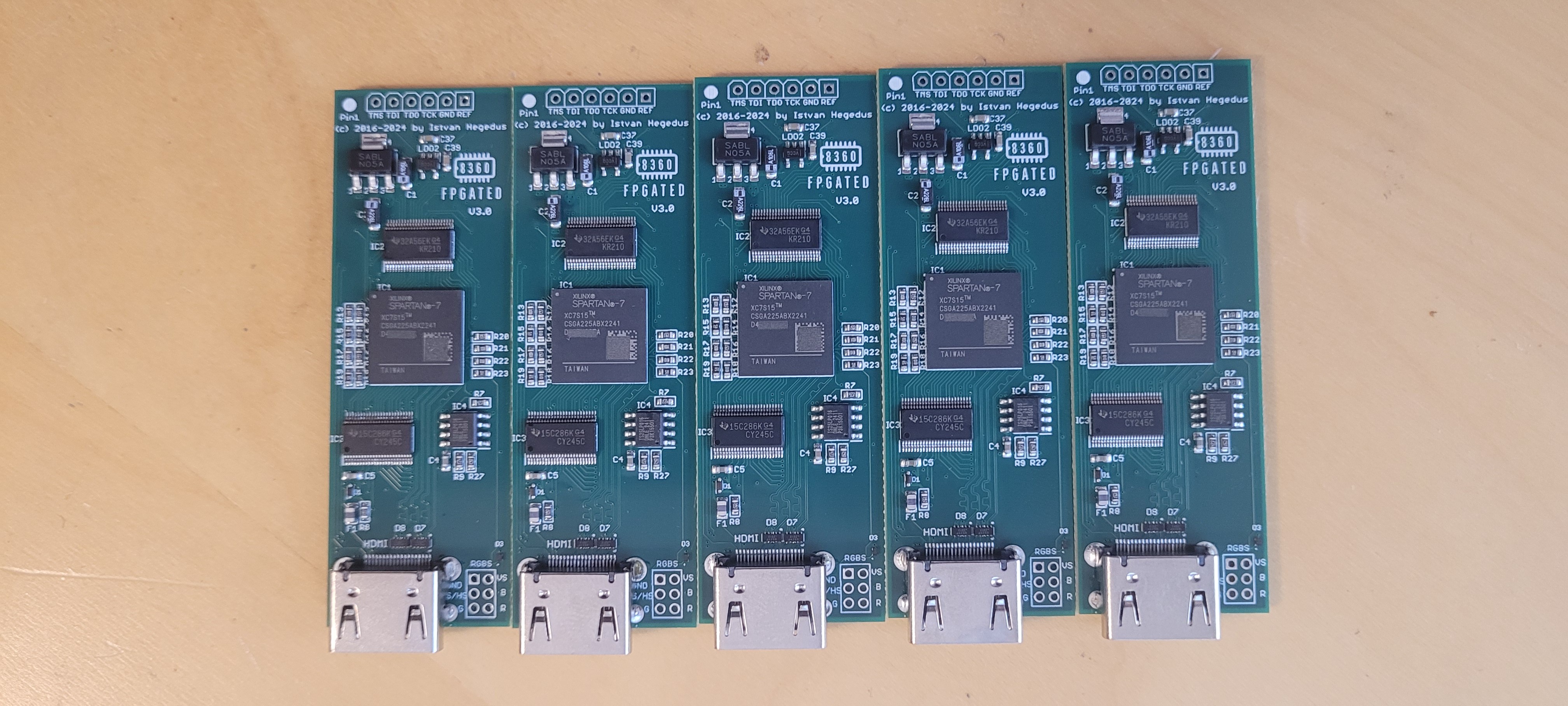
I am glad to announce that I have created a few FPGATED devices (HW ver 3.0) which are available for sale! As this is still a development, these are available in a limited number for those who are interested and are willing to do tests and report any issues.
![]()
The board perfectly fits in a C16 and Plus4, however in the Plus4 due to space limitations a 90 degree HDMI connector cable must be used (right angled to straight).
I use the following one: https://www.aliexpress.com/item/1005006299127375.html
I recommend to replace the 48 pin IC socket of the C16 with a precision one as it requires strong force to insert the board in the factory socket. However if that is not a possibility, it is ok to use in the original socket too.
The installed firmware and SPI flash includes a configuration software I have written, but at the moment using it requires a short starter code that I will share later.
If you are interested please send a mail to info@fpgated.hu for contact and price details.
-
FPGATED HW Version 3.0
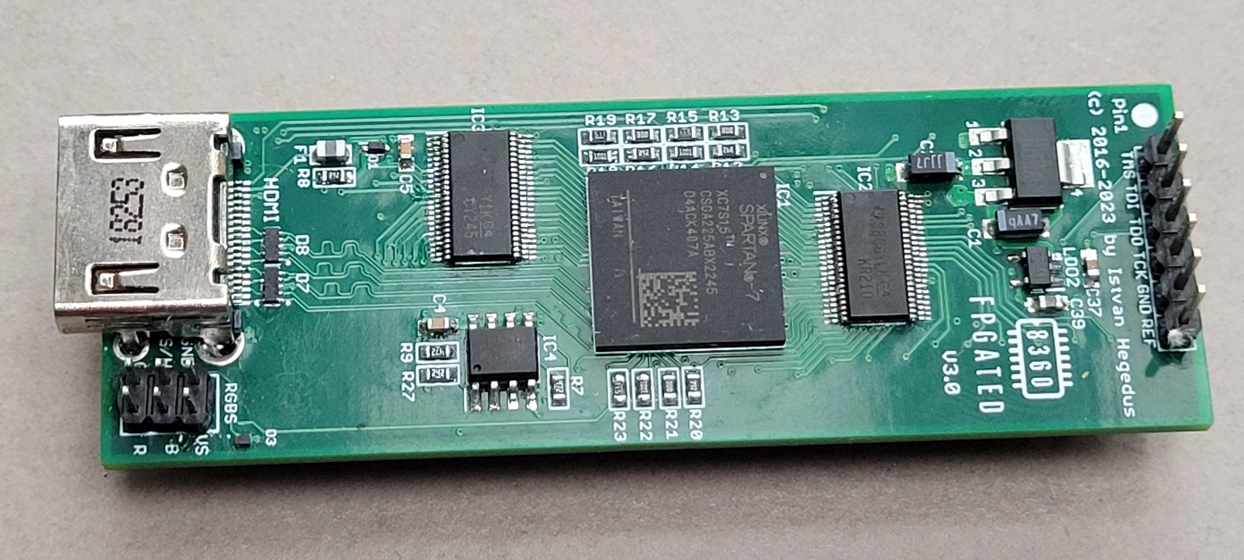
02/22/2024 at 14:05 • 2 commentsAs we have reached the end of chip shortage period I am glad to announce that I have finally finished the HW design and prototype testing of FPGATED. The last years were challenging, especially with Xilinx AMD acquisition and the production stop of Spartan 6 FPGAs. My original design was based on the Spartan 6 FPGA and even though I had two prototypes working, I had to come up with a successor that can be produced for the audience. An obvious path was to use the Xilinx Spartan 7 but as much as it was easy to modify the internal code it was challenging to redesign the PCB for Spartan 7. Hardware version 3.0 is the result of this redesign and I can proudly say that it works flawlessly!
FPGATED HW version 3.0 has the following features:
- Xilinx Spartan 7 XC7S15CSGA225 FPGA
- Most resource utilizations are below 50% thus plenthy of room to add new features!
- Original analog Chroma and Luma output to get picture via RF modulator
- RGB header onboard which is software programmable between 15KHz SRGB and 31KHz VGA output
- HDMI connector with digital output with 720x576/50Hz or 720x480/60Hz output
- Digital audio output on HDMI connector, so you can hook up the C16 or Plus4 to a modern flat TV
- Software switchable scanline effect on HDMI and VGA outputs
- 4 software selectable color translation tables for HDMI, VGA or SRGB outputs (FPGATED Caclulated, Plus4emu, YAPE, Custom)
- 1 software programmable custom color table (out of the 4 tables) to be able to adjust RGB colors (CVBS is not affected)
- theoretically firmware upgradeable from Plus 4 side (but 1 floppy is not enough for firmware)
- ESD protection on HDMI connector and VGA header
![]()
![]()
What is next?
Calculating HW cost and seeking for HW production possibilities. My plan is to start with batches and sell them via e.g. Amibay. Also I am going to write a software to modify configuration registers and the custom color table. The configuration is saveable to flash!
Further development is ongoing to add a SID chip implementation and improve TED core compatibility,
The VGA/SRGB header requires a special cable that will be sold separately (or can be built by anyone).
![]()
-
Hardware revision 2.0
05/14/2022 at 20:10 • 2 commentsDear followers,
I know it has been a long time now I last posted update on this project, however I can assure everyone that this project is not dead. As everyone knows there is a global chip shortage which impacts the commercial release of FPGATED. Unfortunately at the moment the prices and delivery times of FPGAs are not making this replacement a cost effective solution.
In the meantime I have redesigned it to v2 HW version using a smaller BGA chip and a HDMI connector. Also the bus switch I have used is End of Sale so I had to redesign it using TI chip for voltage translation.
![]()
At the moment I am in the challenge of hand soldering it and then test the HDMI output. When ready I will post more pictures and video about it.
After that the production can start and I want to make it available. In order to make it even more cost effective I am planning to shift to Spartan7 FPGA in v3 version (which I am currently unavailable to procure even for prototyping).
Please be patient.
-
FPGATED prototype is working in a C16!
01/14/2021 at 21:06 • 3 commentsHi,
Heading into 2021 here is an awesome news for those who are waiting this moment for 4 years now! I have managed to build the first prototype of the FPGATED IC which is a direct drop-in replacement of MOS 8360R2 IC.
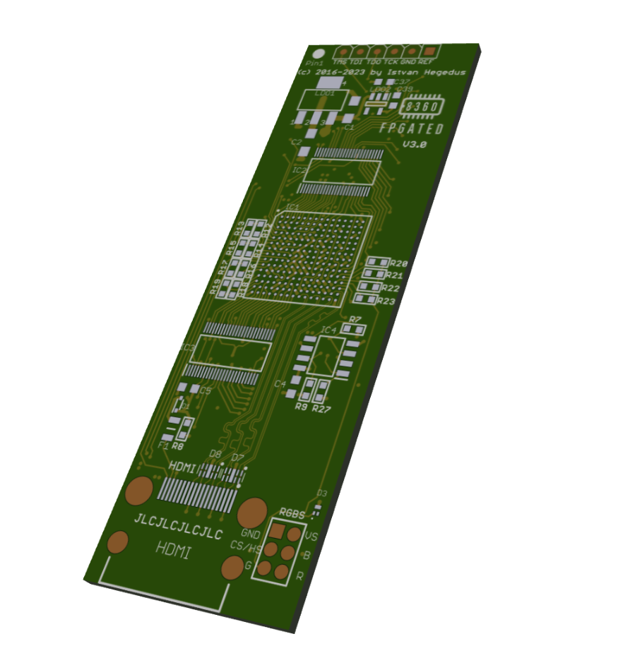
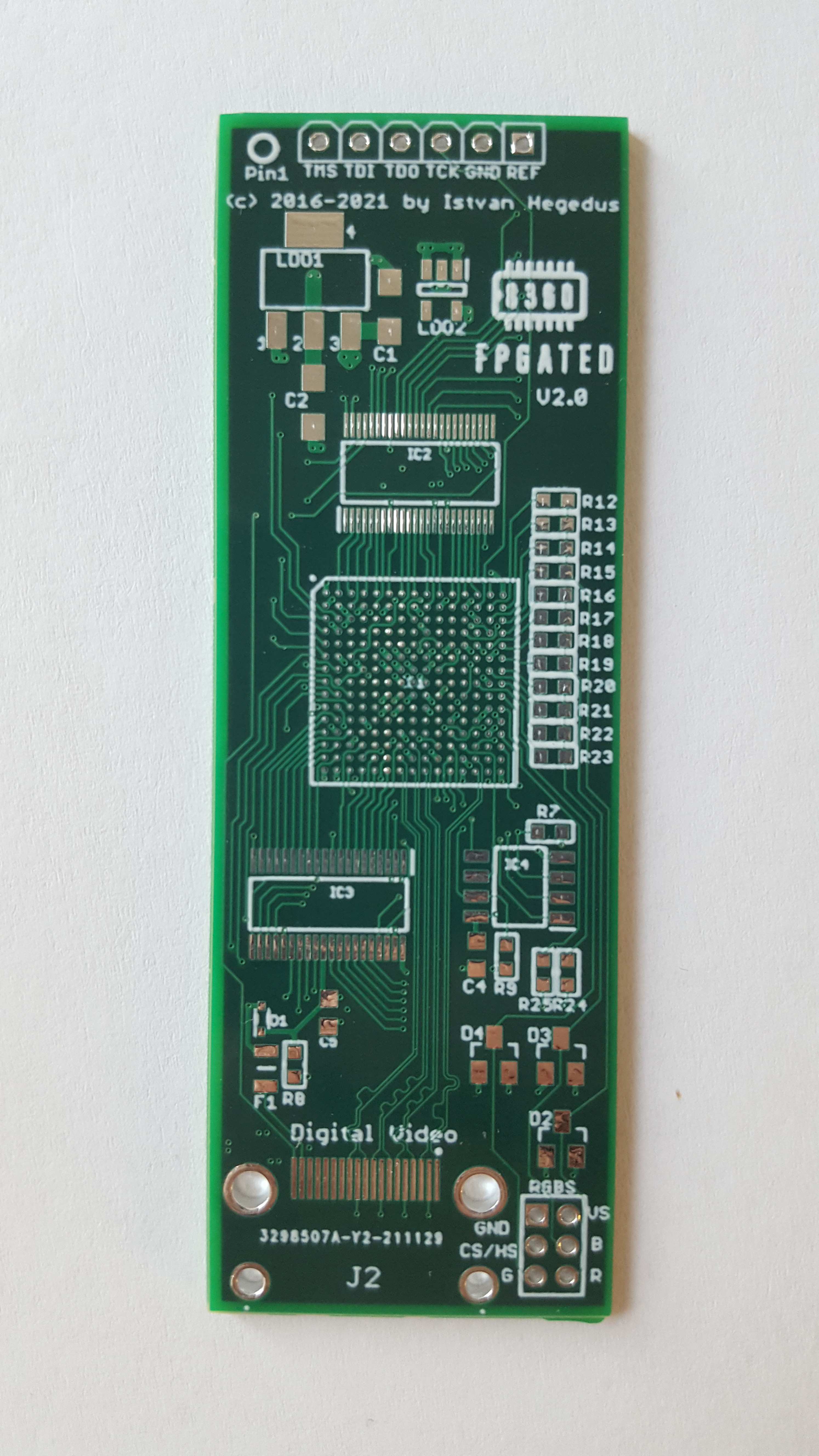
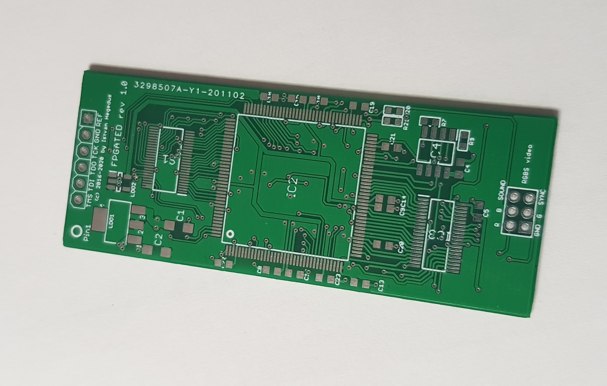
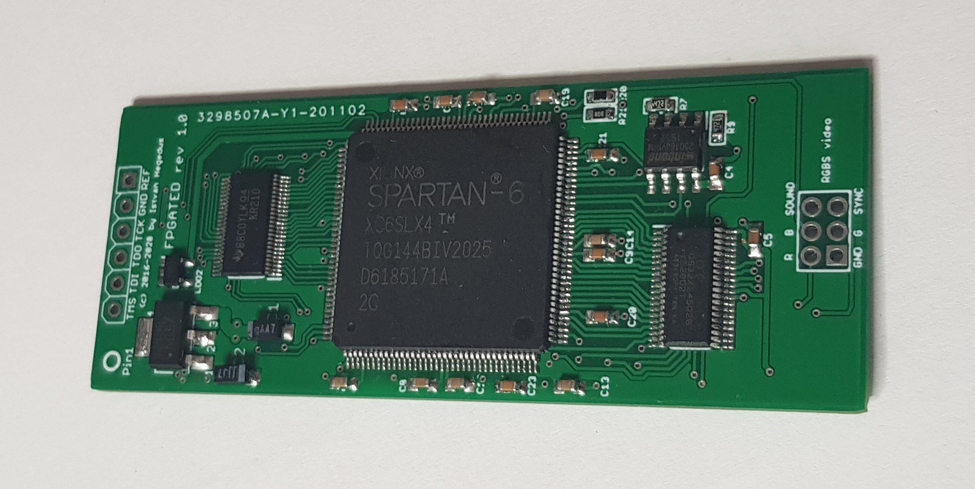
Here you can see how the empty and populated PCBs look like on the top.

RAW PCB Top 
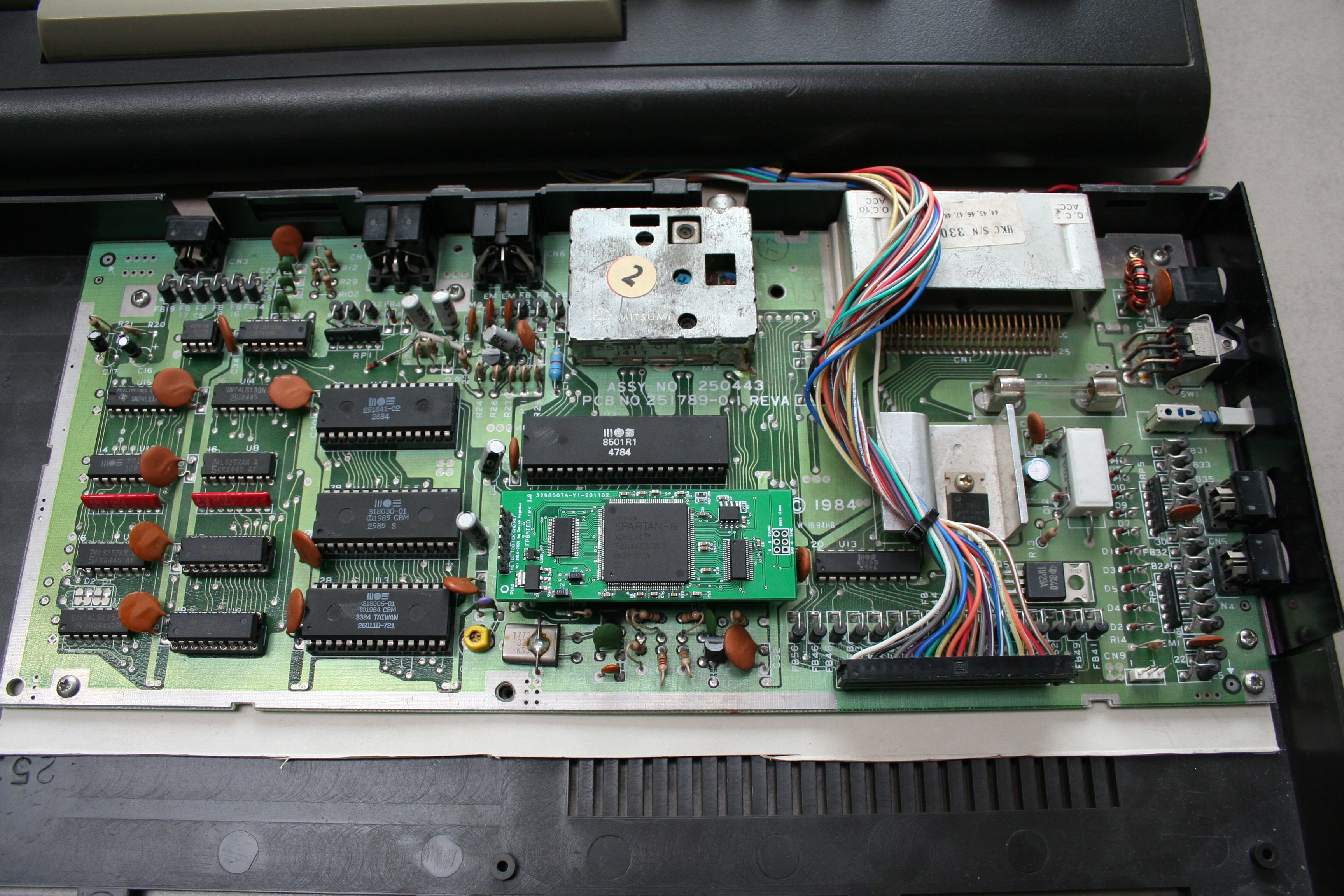
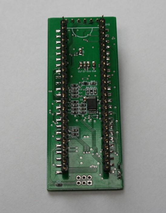
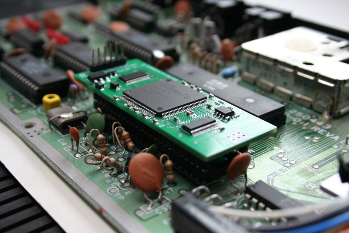
FPGATED top The size of PCB just fits into a Plus4's TED shielding and fits easily in a C16. Although I have tested it in both machines further testing is done using the C16 because it has more space and it is easier to load the firmware via the JTAG connector.
The board has two level shifters for those signals which need it. Outputs from TED's point of view don't need level shifting because they are LVTTL compatible, only bidirectional or input signals are translated. Interestingly the motherboard's clock signal stays under 3.3v (see PLus4 or C16 schematics which gives explanation) so it is directly connected to the FPGA. Two cascaded LDOs create 3.3v and 1.2v supply voltages from 5v. As the 2nd LDO is supplied from 3.3v the heat dissipation is minimal and the component stays cool during operation.

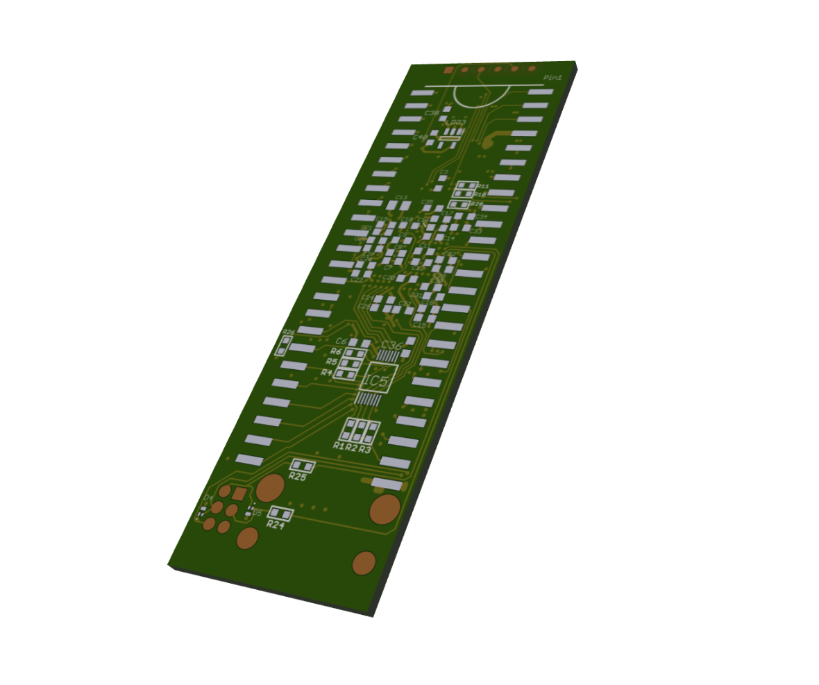
It fits easily Inside a C16 The backside of the PCB has an SMD IC header which together with the FPGA are the most expensive parts of the whole device. To keep cost as low as possible a Xilinx Spartan6 LX4 FPGA is used which still have empty space left inside for further improvements, but it can be replaced by an LX9 if needed (of course not by users). As the SMD IC header has still not yet arrived I had to create a temporary solution using straight through hole IC headers. As these are for through hole applications, the shorter pins which are normally soldered inside the PCB holes are now soldered to the smd pads. Benting them would break them so this was the easiest way to test the device without the final header. I was surprised how solid it is when soldered! The only drawback is that the device is now too high when inserted to the TED socket (which is not an issue in a C16, but might be problem in a Plus4). But hey this is just a prototype!

Back side of the PCB The components I have soldered with my hands (takes time but not that difficult when you have a microscope).
I was afraid that during power up the configuration of FPGA will not finish by the time the reset cycle finsihes (about 500ms), so in the design I have taken this into account. In order to speed up the configuration time during power on, the onboard SPI flash has a quad connection and the bitstream utilizes it with a 10Mhz configuration clock. Needless to say that it works perfectly!
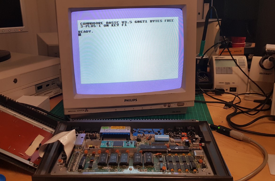
I have programmed it via iMPACT and turned on the Plus4 with high hopes (yes, first I have tried it in a Plus4).

First power on in a Plus4 It works! Thanks to the careful design, individual part testing it works perfectly! The image is generated via the composite video out and RF modulator (I was surprised how much better the Plus4's RF modulator is compared to the C16. It gave much sharper and clearer picture). I have adjusted the color phases to be as close to the original as possible, I have even done measurements on real TED via oscilloscope and calculated phase angles from time differences between burst and color signals.
Since the first power on I have used it a lot and tested serveral games, demos. I have fixed DMA delay in TED core (see release latest source code) and now everything I tested so far works fine!
So what are next steps?
I am waiting for the smd IC pin headers and can build some more units (I have components for about 10 now), The PCB has an SRGB header also which I have not yet tested. What I regret is that this header does not have hsync/vsync just csync. So if I want to implement scandoubler I need to redesign this part.
- I am going to design a 4 layers PCB for the cheaper and smaller BGA Spartan6 using through hole pin header (v2).
- Create a mass production so that everyone can buy it
- VGA output
- HDMI output
- SID cart implementation inside the FPGA
Soon I will create a youtube video about how it operates and share its link here on hackaday.
Until that keep your eyes on the updates!

Installed in a C16 -
FPGATED hardware rev 1.0
11/04/2020 at 21:23 • 2 commentsFPGATED hardware prototype is now in the finish!
The schematic and board layout was finalized, ready for PCB manufacturing.
![]()
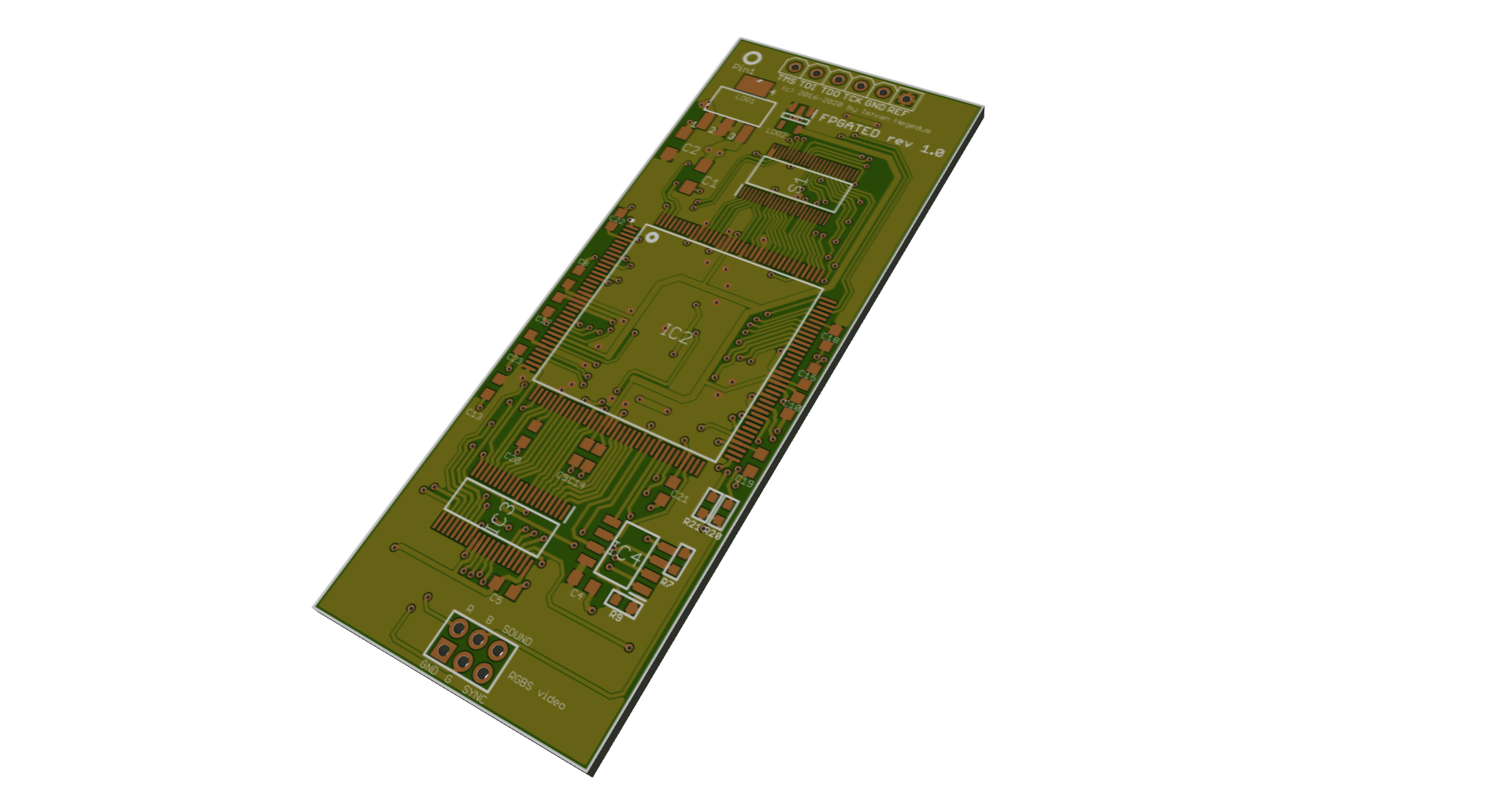
This is hardware revision 1.0 using a TQFP144 Spartan6 FPGA. It is only a 2 layers PCB so most probably rev 1.0 is not the final production one. The main goal is to test all functionality in a C16 or Plus4 and then shrink it even further.
The production version will use a smaller BGA package FPGA with 4 layers PCB and cheaper IC socket connector. This one features an SMT mounting socket connector at the back in order make space for the TQFP144 on the top. Good news is that I have managed to route the RGBS signals to a small 2x6 connector on the top, so besides composite, RGB video signal will be available too.
I am now sourcing components but 2 items on the list has a bit longer lead times than I expected, so expect it running in Q1 2021!
Stay tuned!
-
TED analog part implemented
06/12/2020 at 15:55 • 0 commentsI am glad to report that the analog picture generation part of the drop-in TED replacement is ready!
The luminance signal is implemented with a look up table and a smart external circuit which is not a DAC so it generates perfect voltage levels for the various luminance signals (I don't want to release the circuit details at this point).
The chrominance signal was easier than I thought, however the DDS phase accumulator I had to increase to 24 bits because it turned out that the PAL standard requires very precise 4.433618 MHz frequency. Unfortunately I cannot test NTSC as I don't have an NTSC monitor but I am implementing that part too! I will leave that later for test users from US region.
To test the result I have created a PAL test screen top module which generates SMTPE bars and/or different color bars that I can change in code. The FPGA board I have hooked up to a C16 motherboard via TED chip socket's Sync and Color pins in order to see the real composite output on my monitor. The result pictures speak for themselves.
![]()
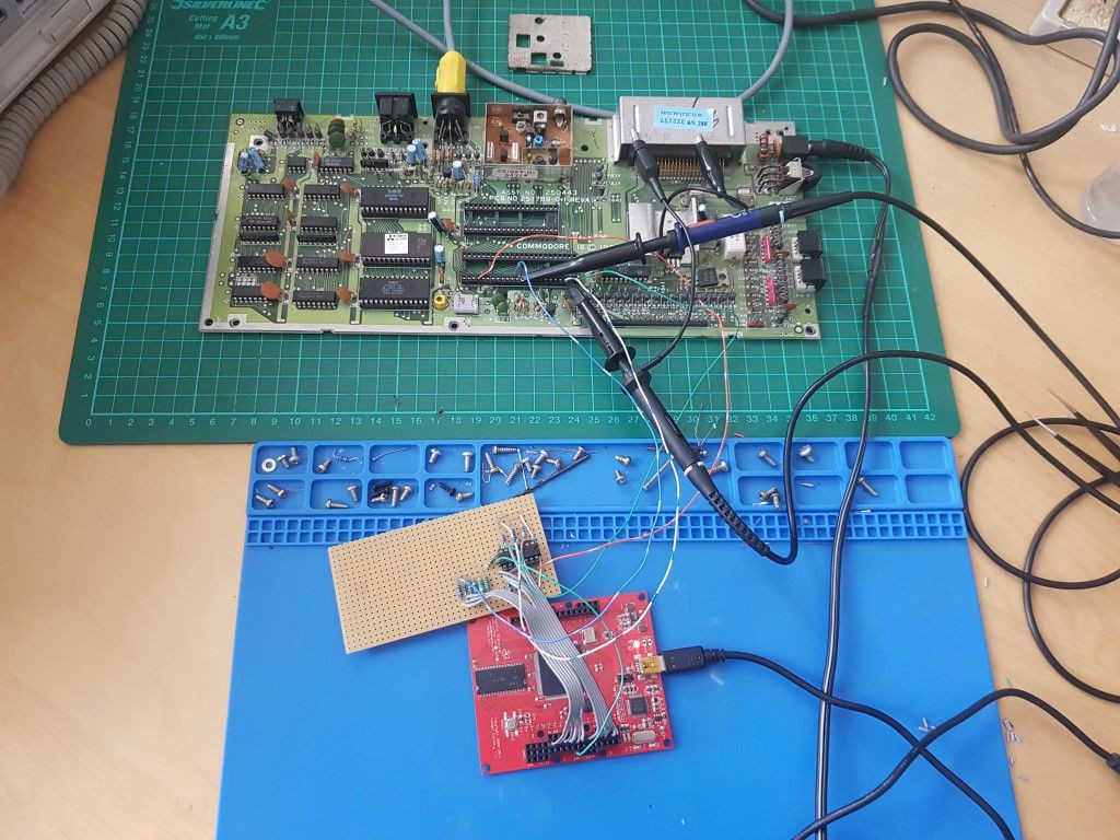
This is my testbench using a Papilio Pro board and some analog components on the test board.
![]()
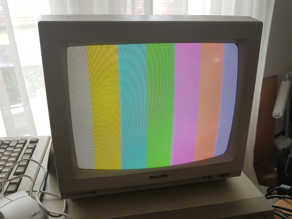
SMTPE color bars generated via the FPGA and C16 RF modulator.
(those moisters are visible only on the photo, but in real life they are not visible)
![]()
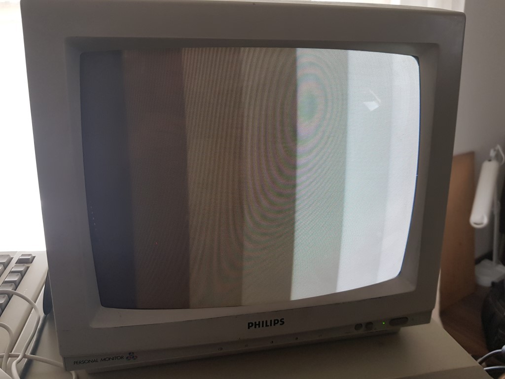
Testing luminance levels with white color (grayscale).
![]()
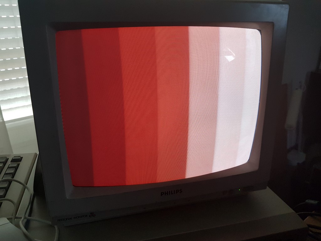
Same luminance test with red color bars.
Next step is to start to design the PCB! It will take some time as I have never designed a 4 layers PCB with BGA chip on it. Current FPGA choice is Spartan 6 LX4 or LX9. My goal is to keep cost as low as possible to create a competitive chip in price.
-
Drop in replacement progress
05/13/2020 at 08:38 • 0 commentsUpdate on FPGATED drop in IC replacement.
The drop-in TED replacement's biggest challenges are
- the analogous part of the IC (Luma and Chroma generator)
- component sizes on the PCB to fit the small space in the Plus4's metal cage (C16 is not an issue)
Over the last months I have been investigating these and created some proof of concepts. Unfortunately I had to rule out the using of an external video signal generator like the AD724/AD725 IC because the RF modulator of Plus4 and C16 delays the chroma signal too much (about 100ns) which requires a luma delay circuit to get them in phase. Delaying an analogous signal is much more difficult than delaying digital one thus I have turned to a different approach.
The luma signal can be created relatively easily in the FPGA using LUT for the luma values and requires just a few external components (resistors) before connecting to the RF modulator. Here the only challenge is the external voltage levels which should be between 0 - 4.8v. This part has been solved.
The chroma signal requires DDS to create the sine wave and modulate its phase. This is not too difficult either, however it requires some careful planning in order to have an optimal design and not to over complicate things. Some of the questions are, how large should be the phase accumulator and the DAC resolution? Do we need a high precision DAC? What should be the internal clock frequency for the DDS keeping in mind that we need to implement PAL and NTSC both? I have done simulations in Matlab which shows some good results using 12bits phase accumulator (no truncation) and 6 bits DAC.
Again the biggest challenge is how can I fit all these components to the small PCB? I need to find an optimal FPGA in physical size, most probably with BGA package.
TED module needed some modification too because I have not yet implemented the burst signal which is also handled by the horizontal events decoder. In addition an output buffer enable signal is needed from TED to signal when it puts data to the databus (e.g. when we read one of its registers). This signal controls the FPGA's bidirectional data bus IO pins and not available on the final IC legs.
The result will be shared when it is the right time.
-
Bug fixed FPGATED core released
10/04/2019 at 15:36 • 0 commentsImproved FPGATED core is released now!
After a deep inspection and debugging I have managed to identify a bug in the DMA fetch pointer latch mechanism which has caused some FLI/HFLI pictures not shown correctly. The problem is fixed in the new (v1.1) ted.v core and added FPGATED v1.2 download. In addition the c16.v core has better PLA implementation for ROM chip selects which now resembles the motherboard schematics. This might further improve compatibility with software/demos.
If you are interested in a Plus4 implementation using Papilio Pro FPGA then read the previous project log and check out the sources at Github!
Now its time to work on the drop-in replacement board to test the core in a real C16 or Plus4!