Arthur Admiraal
-
Mechanical design
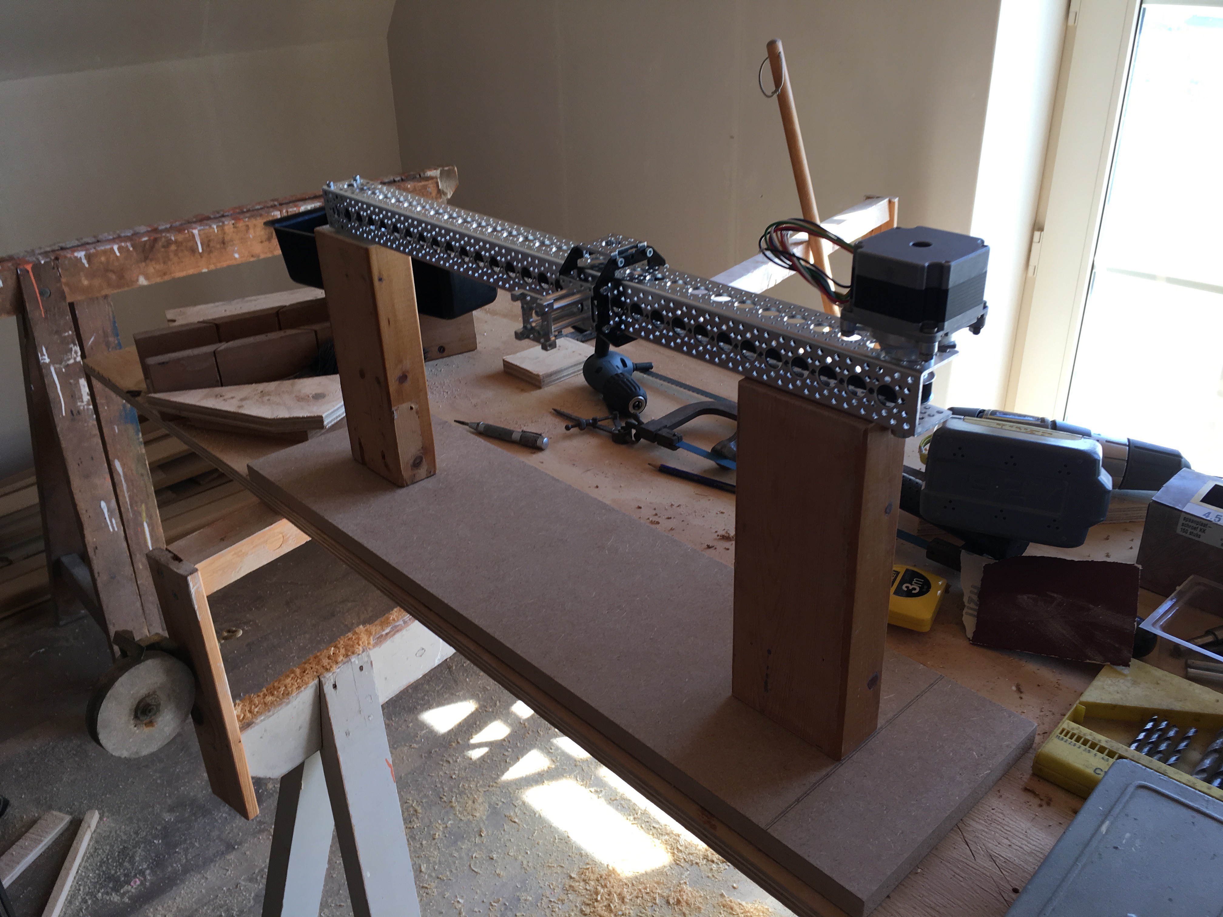
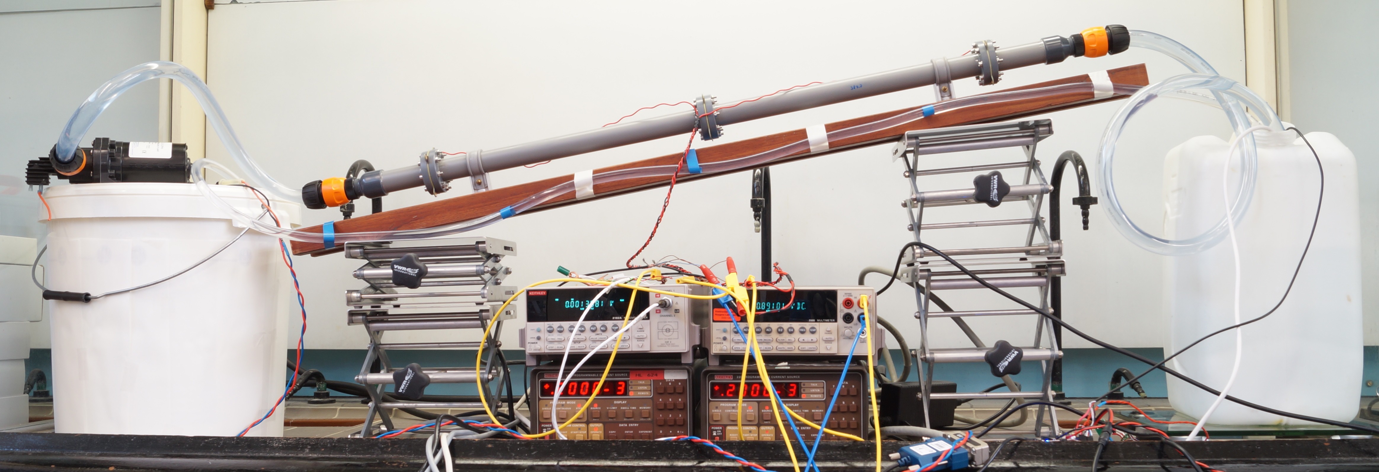
07/22/2016 at 11:13 • 0 commentsAs of writing this log, the build is finally completed, which allows me to talk about the design decisions concerning the mechanical side of this project, since I now have the photographs to illustrate them. In this post I will only talk about what connects to what, details will be provided in the building instructions.
![]()
Construction
The base
Let's start with the base. Al this needs to do is provide some stability and hold up the rest of the setup high enough to slide through a reservoir of a testing solution, not the floor. Hence, the base just consists of a long, rectangular piece of plywood, in which two thick pieces of wood are screwed.
![]()
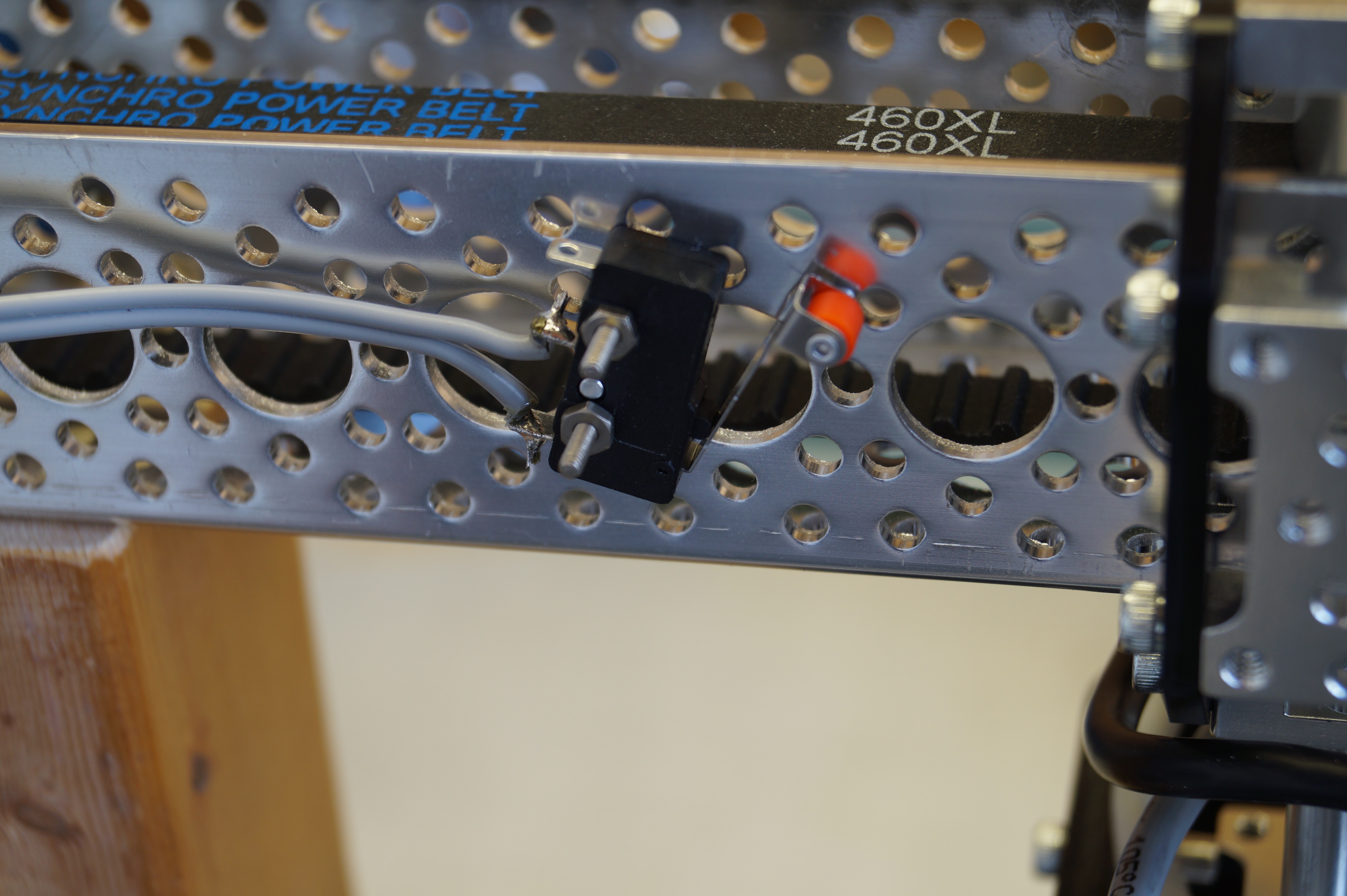
The slider
The slider is attached to these pieces of wood using some wood screws. It is just a regular actobotics slider kit, although I have made a couple of minor modifications.
![]()
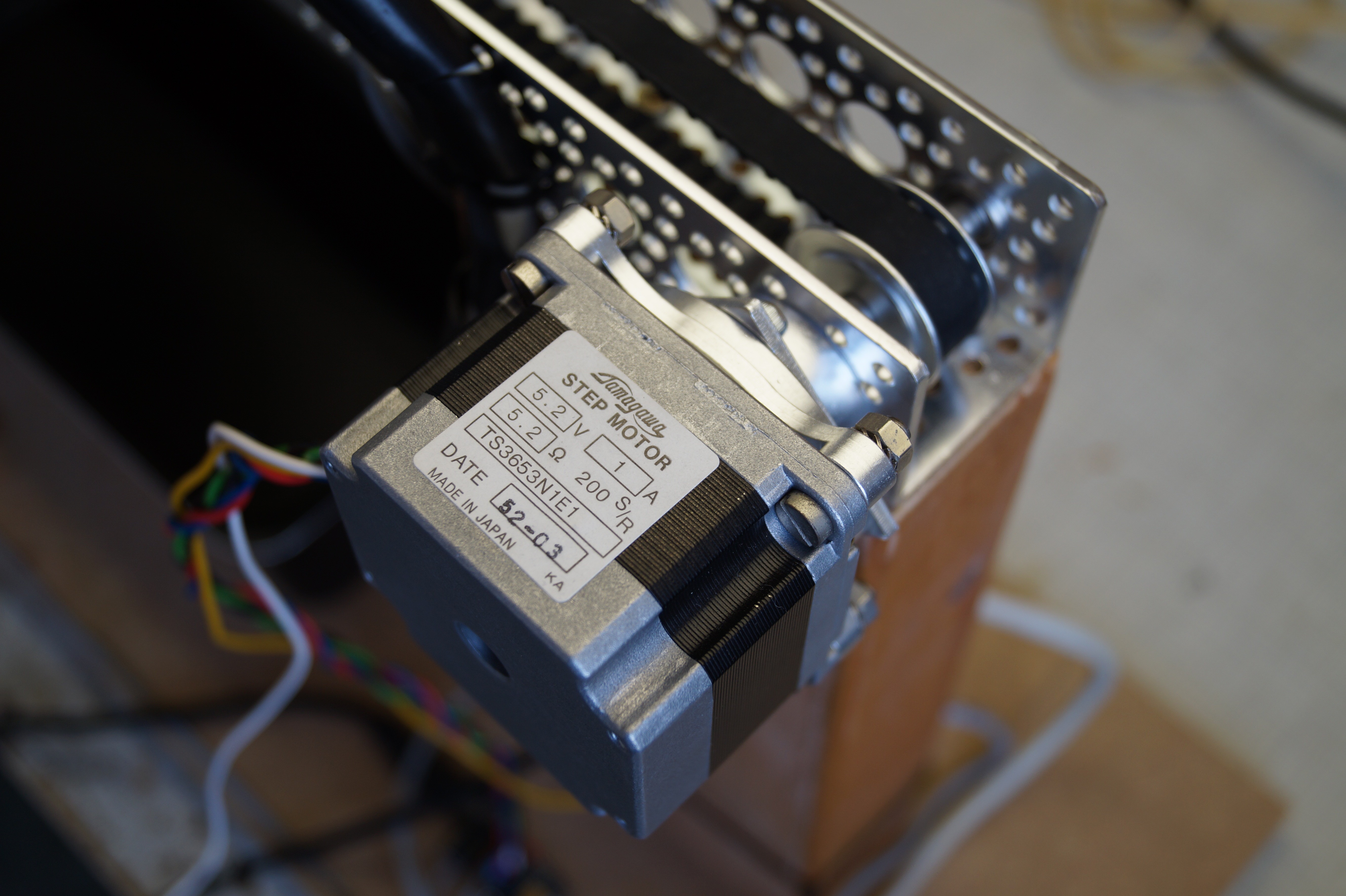
I have used a stepper motor to drive it instead of the usual DC motor. Using a stepper motor allows for precision repeatable positional control, and thus also precision speed control. Because of this, they are generally used in precision applications, such as 3D printers and CNC machines. Since I want the experiment to be repeatable, I thought it was appropriate to use one here.
![]()
Obviously, I have left the feed off, since they would get in the way of mounting it to the base.
![]()
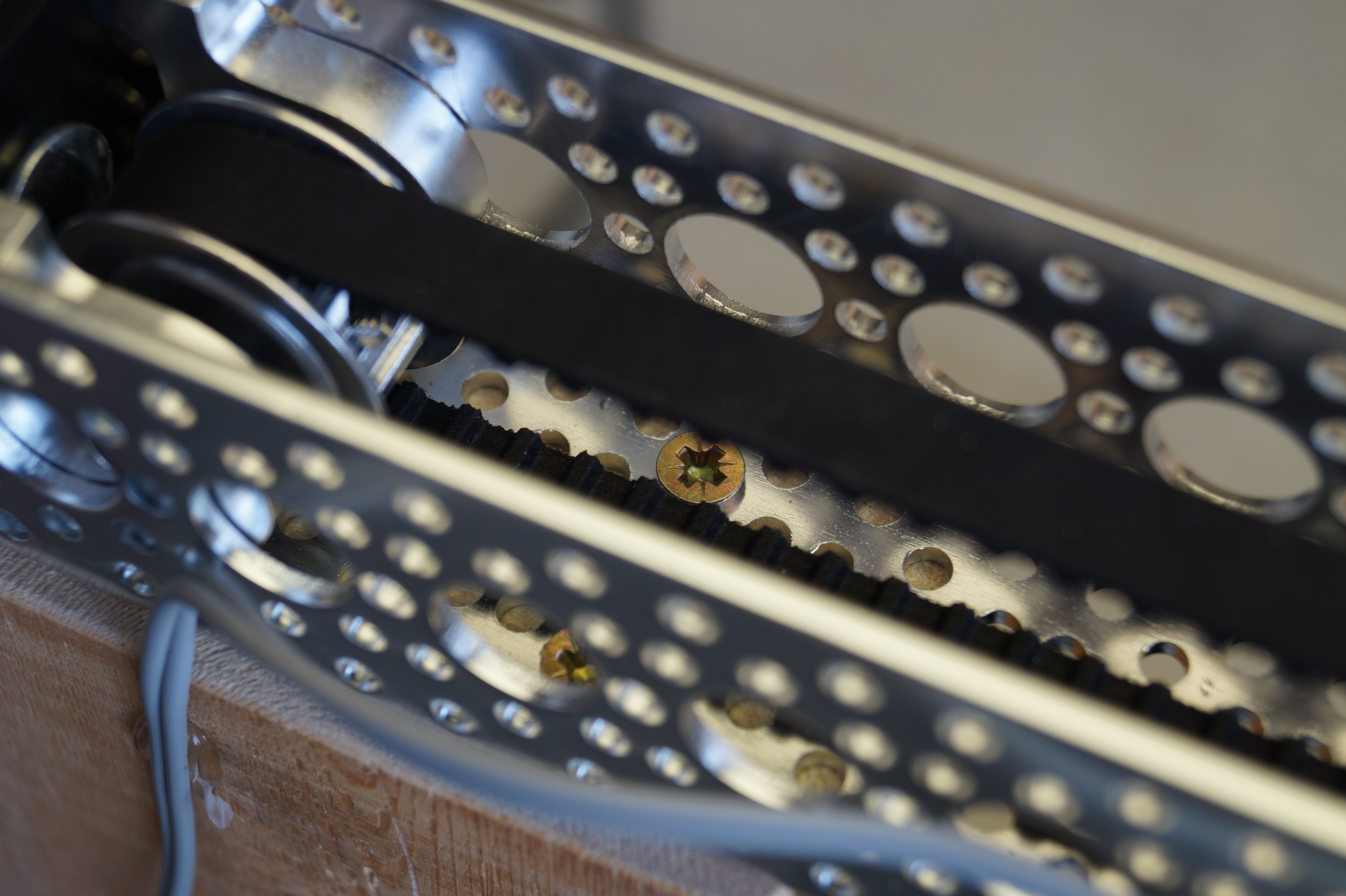
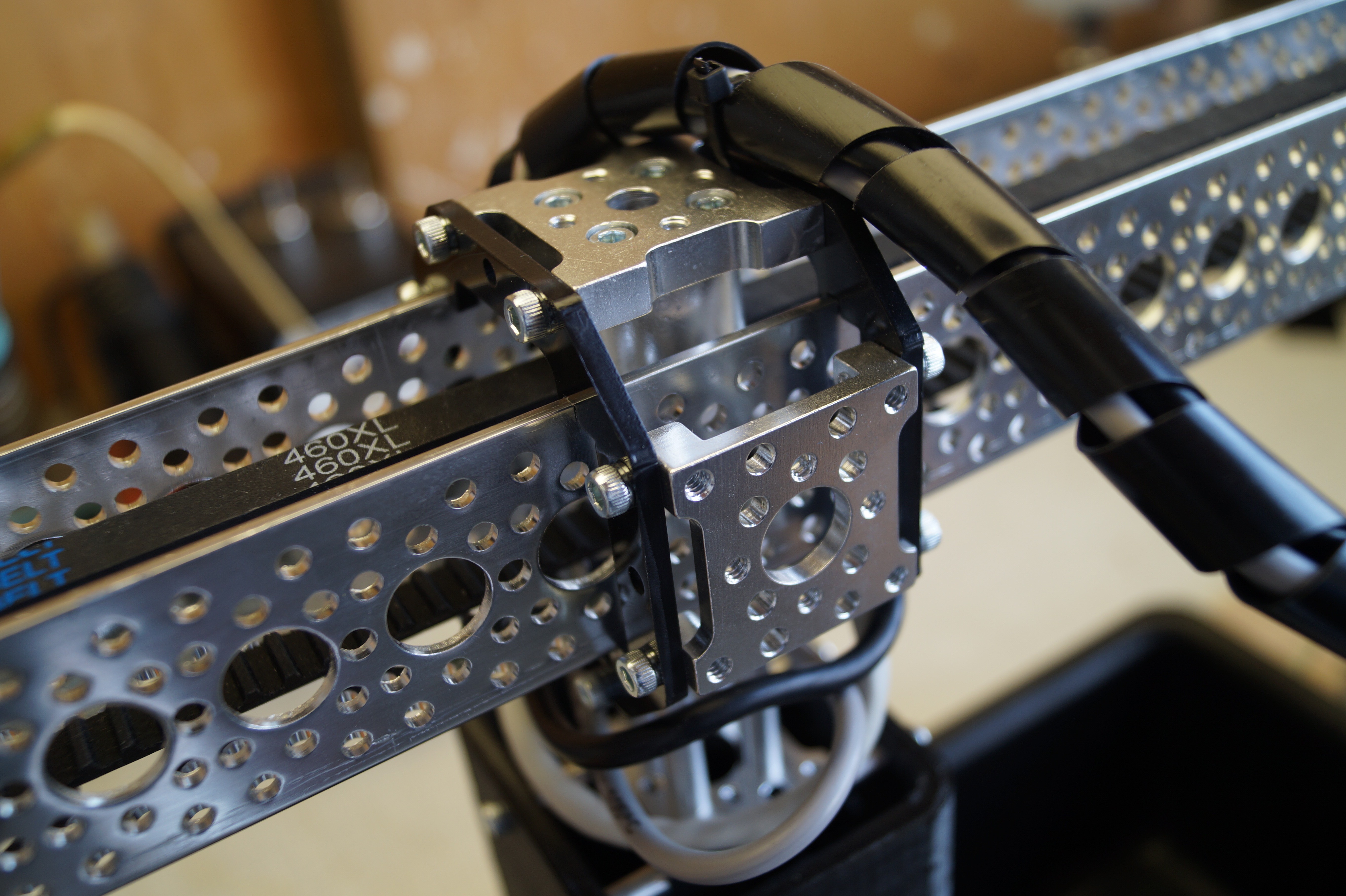
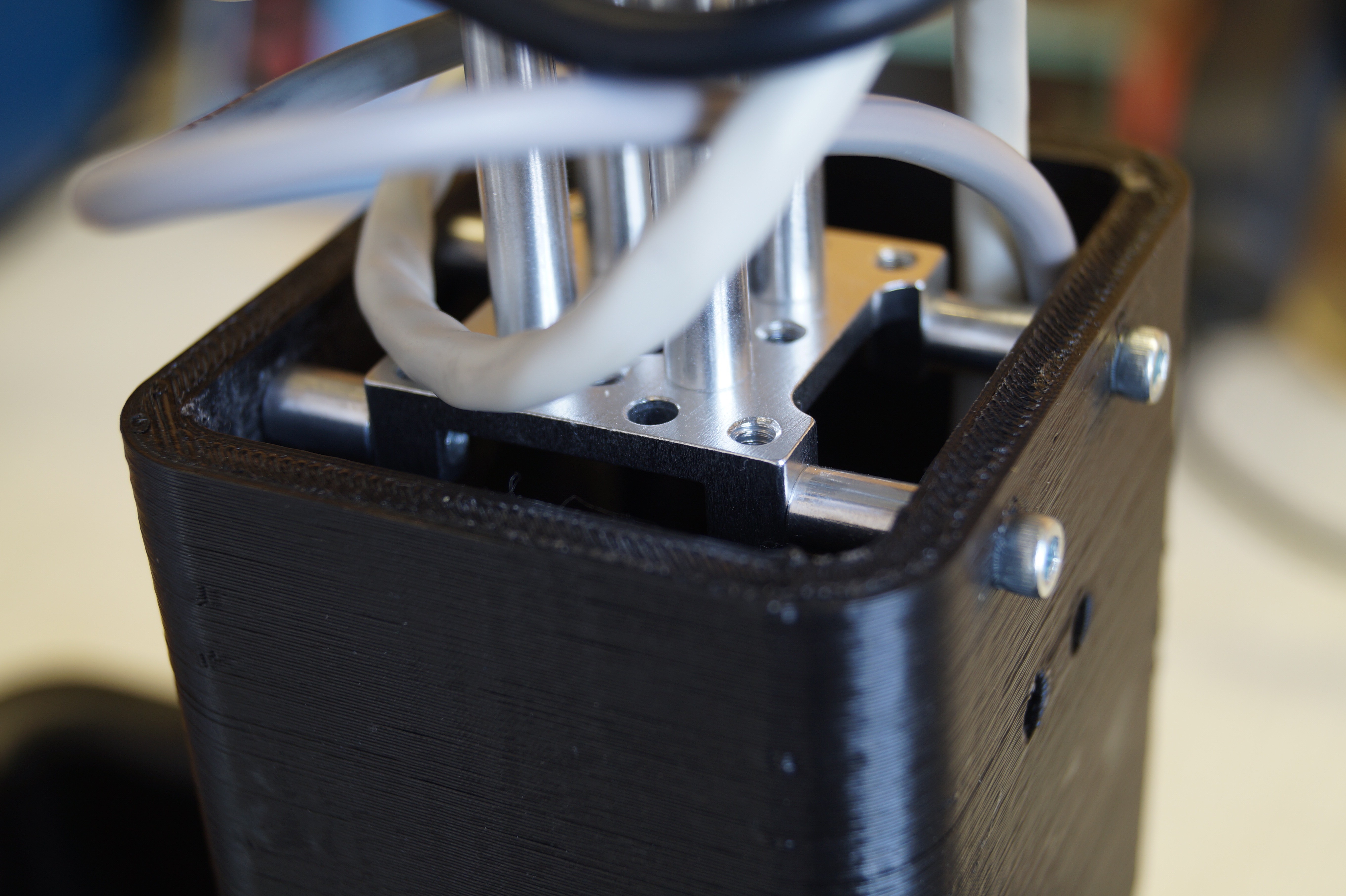
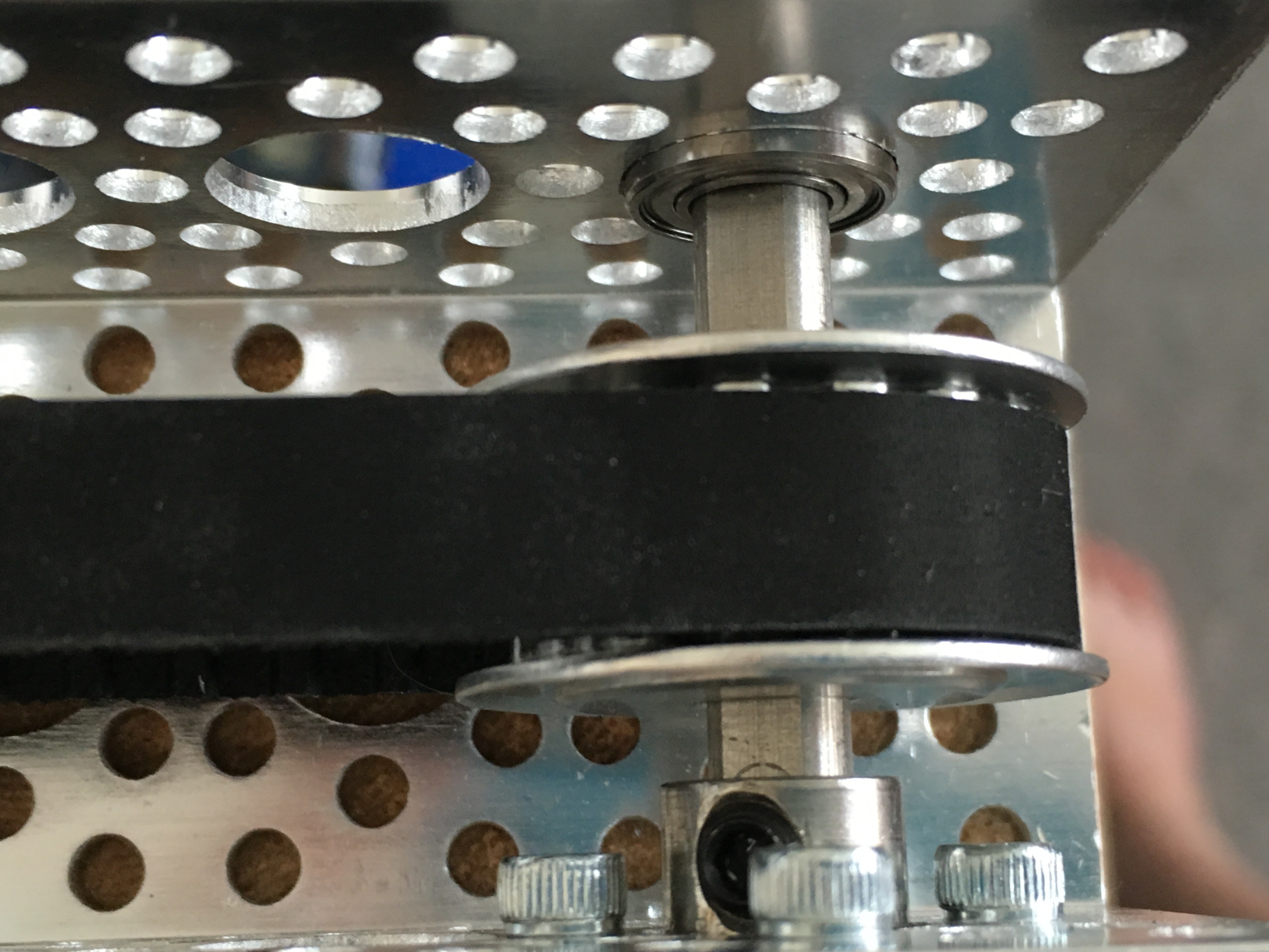
Lastly, instead of the sliders D that came with the kit, I used some channel sliders A and 2 additional hub mounts to create a more solid structure to slide around the aluminium channel, which also has mounting points on the underside. Using some 1.32" standoffs, another hub mount is mounted to this bottom. By sawing the head off some screws, I was able to create male to female standoffs, which I used to mount RISA to this slider assembly.
![]()
RISA
![]()
The construction of RISA is the the most intricate, but still very straightforward. I wanted to be able to disassemble it, so I could make modifications if necessary. It also has to be at least somewhat waterproof, as the the electrode array will be submerged. Let's go through the design from top to bottom.
![]()
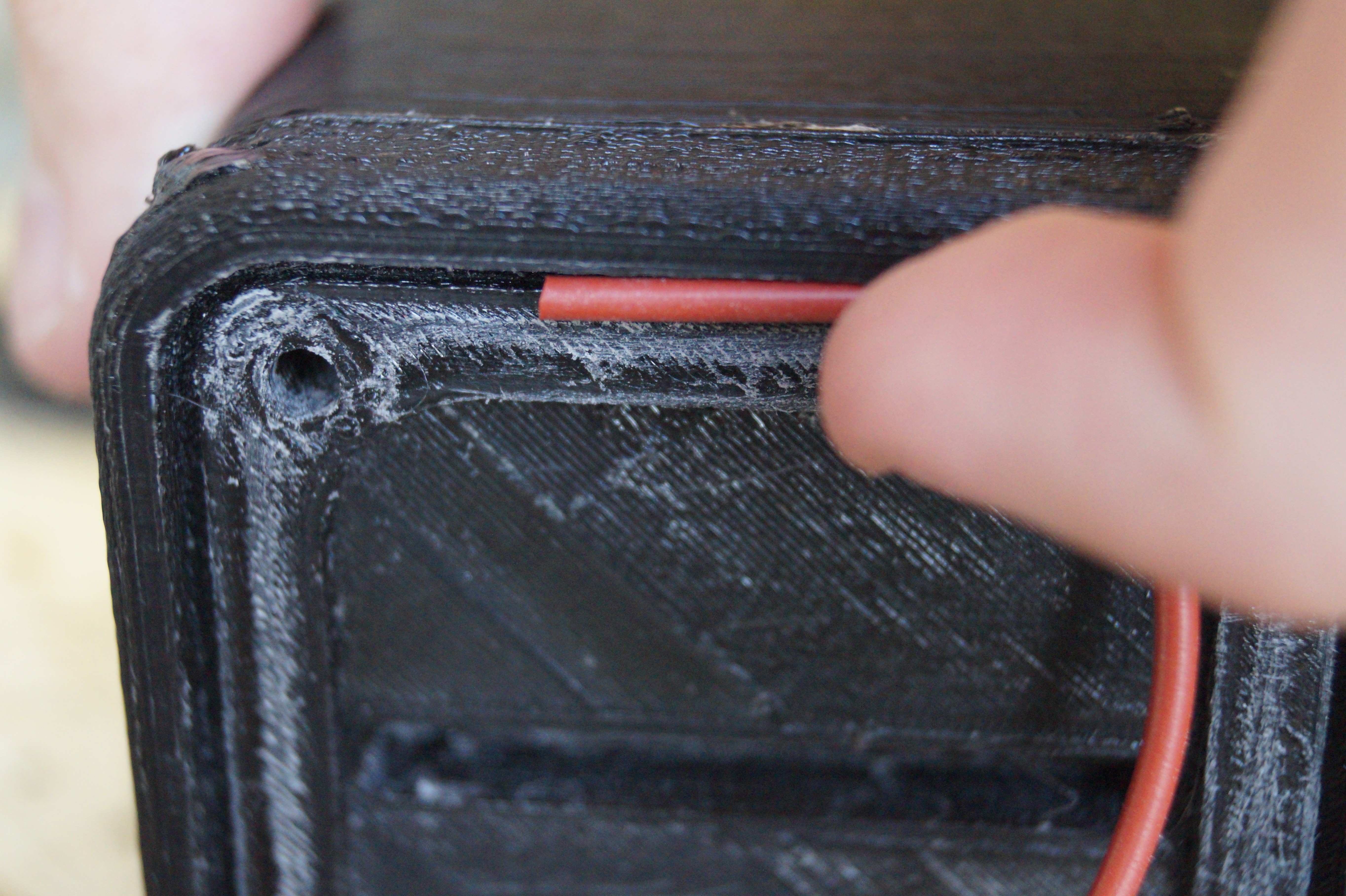
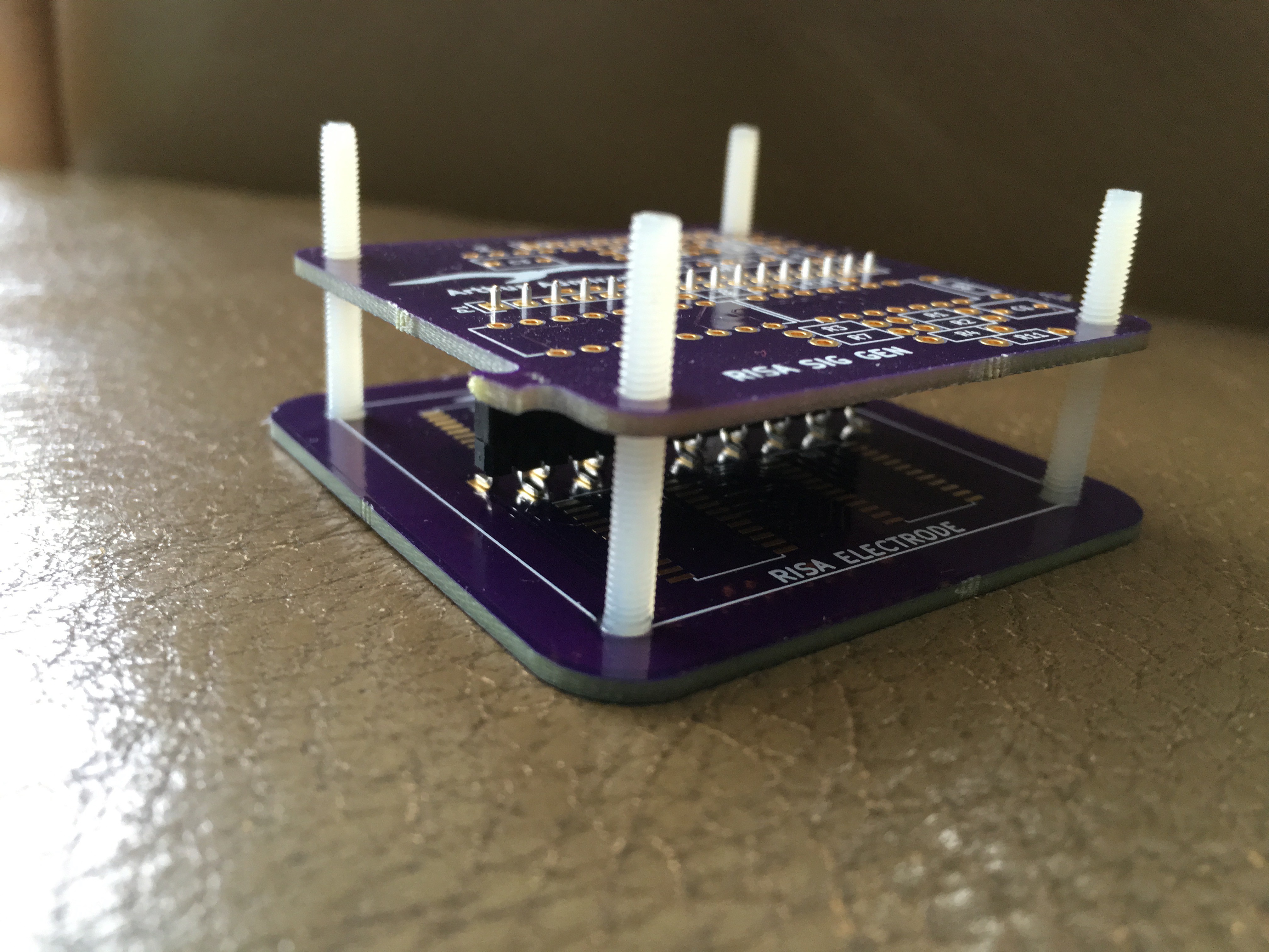
At the top of RISA, we find some mounting holes, 4 on each side. There are this many so that it could also be used under a 45 degree angle.Next, there is a shaft, through which the signal generator PCB can be slid into position.
![]()
There is a slight widening of the shaft, to provide enough space for the USB connector connected to the teensy. I couldn't find anything smaller, so I had to make this compromise.
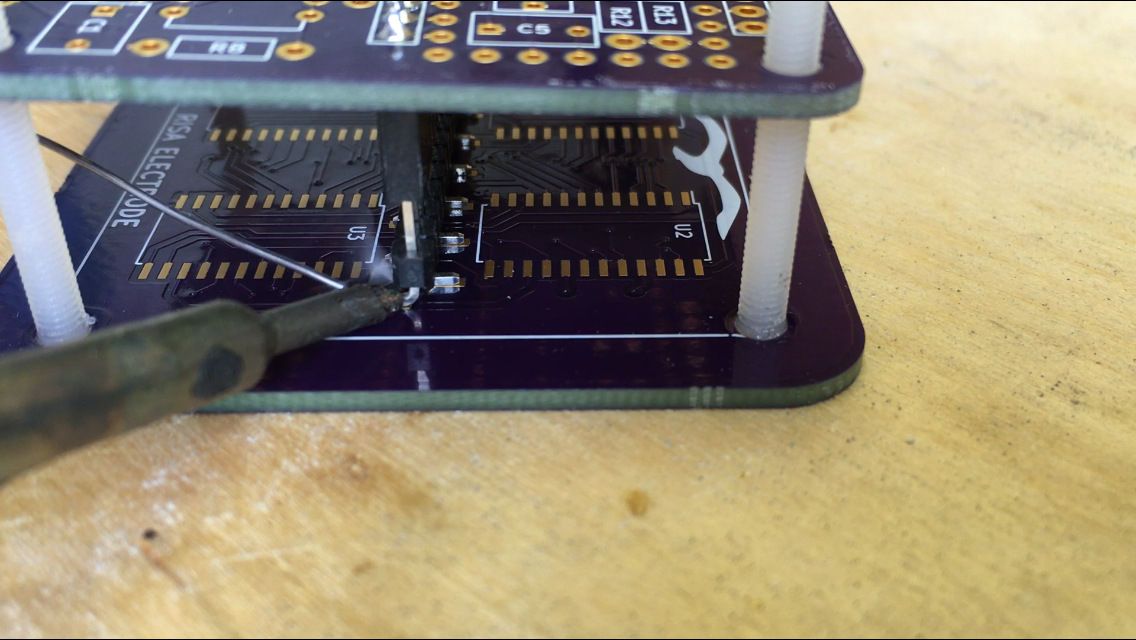
The electrode PCB has a pocket on the bottom of the part in which it sits. The two boards are connected by a .1" header, which connects through a slid in the part.
![]()
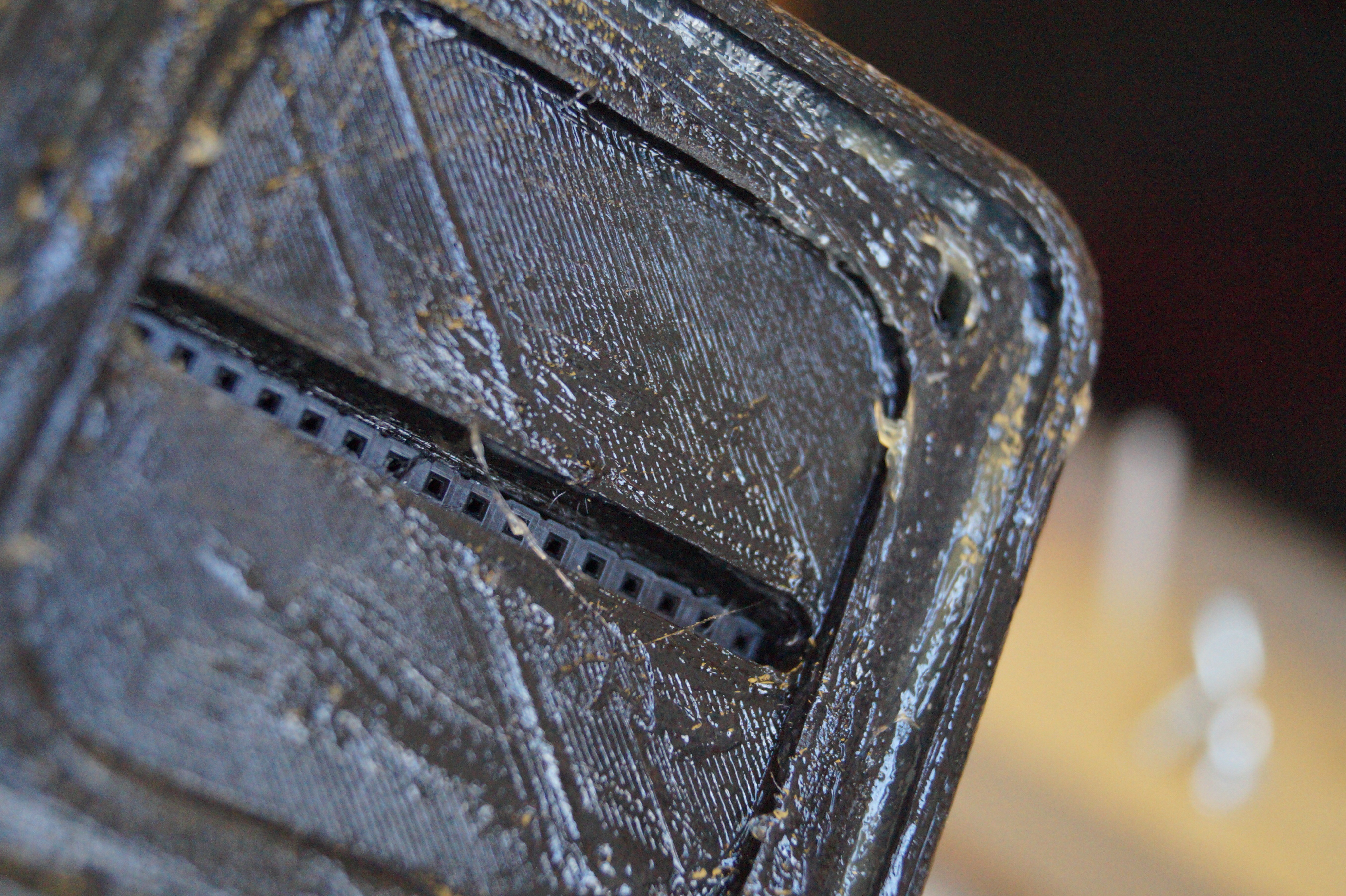
Notice how both PCBs have an additional pocket under there mounts. For the electrode PCB, this provides clearance for the SMT parts on it's backside, while the pocket solely provides clearance for the solder joints on the bottom of the signal generator PCB.
I planned for the boards to be held in place by 4 bylon countersunk screws, which would be glued in place so the assembly would be waterproof. Some nuts would then screw on them on the signal generator board to sandwich the whole construction in place. It was important to use countersunk screws so that they wouldn't disturb the laminar flow during measurements. They had to be some type of plastic to prevent the metal releasing unwanted ions into the solution or influencing the conductivity of it.
I had to countersink the holes in the electrode PCB myself, since the low-cost PCB manufacture services I know of don't provide countersunk holes.
However, I didn't leave enough space for a nut close to the headers of the Teensy, so that it would become difficult to use them. I decided to just screw them in and use some grease for waterproofing, since the seal doesn't have to handle any pressure. On my prototype 3D-print of the part, they tapped themselves into the part, so that I didn't even need nuts. On my second run of parts, this didn't work however. They do provide some clamping force, but not very much.
I was planning to use an O-ring to seal the electrode PCB, but it didn't fit in the 3D-printed part. This meant that I didn't need all that much clamping force so that the headers on the PCBs seem to provide enough force to hold everything together.
![]()
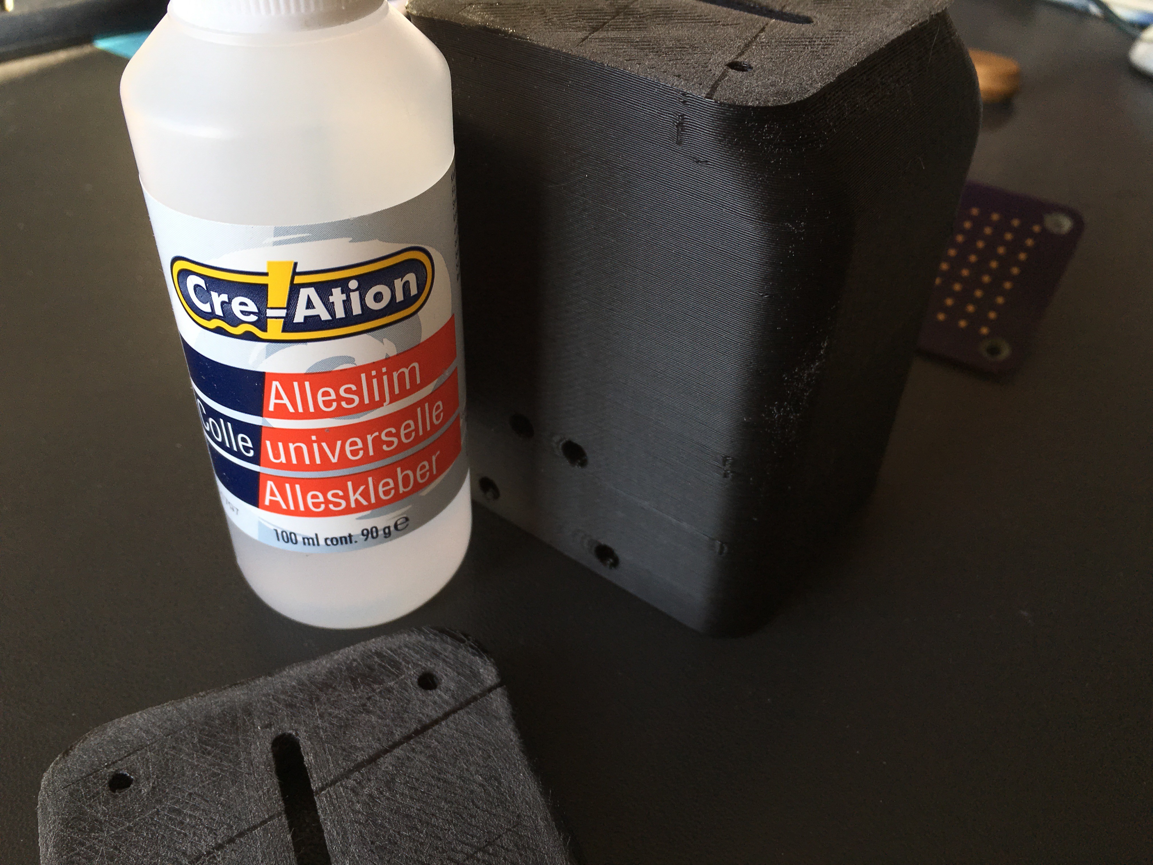
I could reprint the part or file a nut down, but I want to get something working fast, so I decided to just put a lot of grease on the seal and call it a day.
![]()
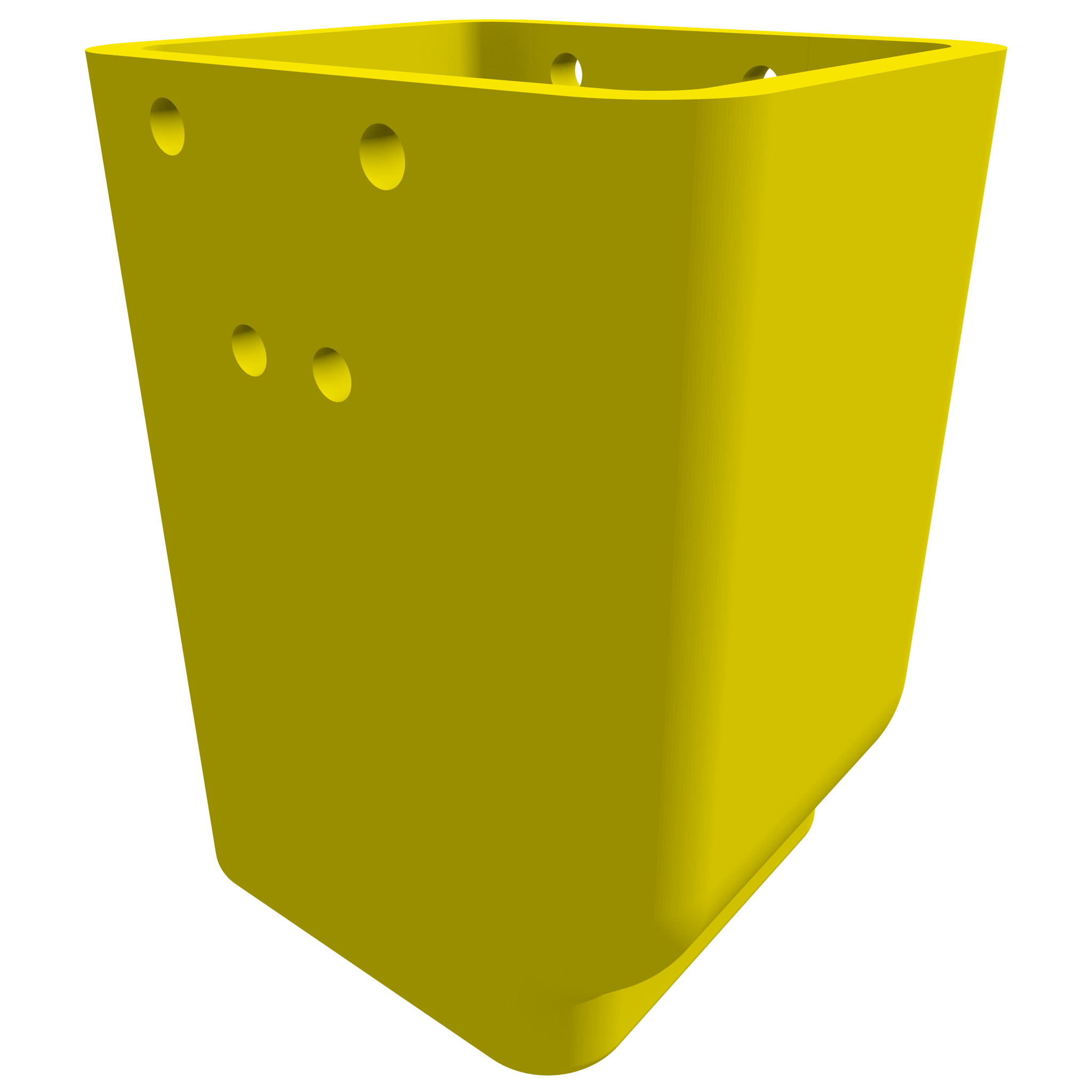
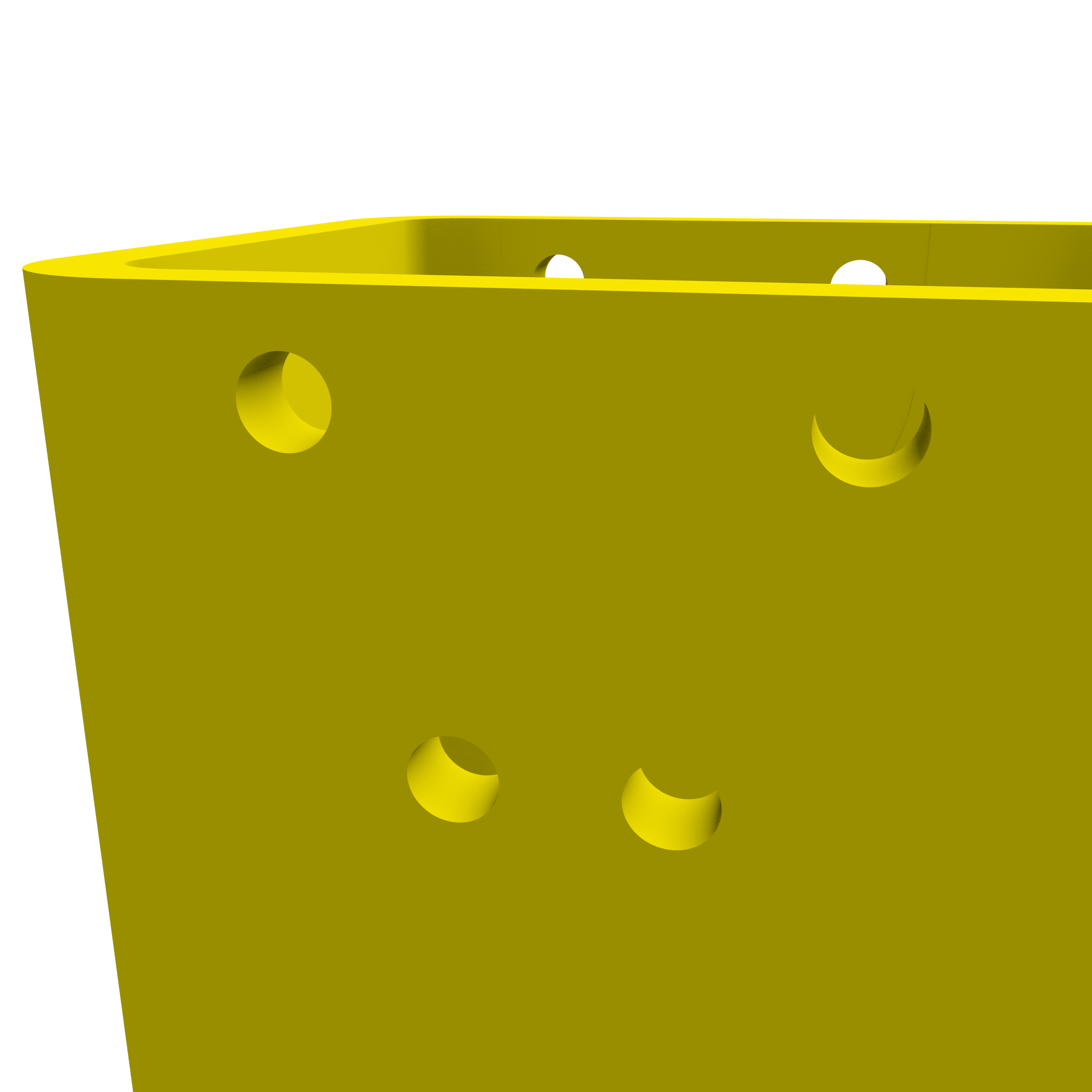
Another interesting aspect of the design is the rounded corners. These have been made so that the flow is as laminar as possible. Furthermore, I 3D-printed this part, but you may have noticed that it has cutouts on both sides of the parts, so that it becomes almost impossible to print on entry-level 3D printers. Because of this, I printed the top and bottom of the part separately, and glued them together later. Unfortunately, I haven't quite perfected my 3D-printing, so that the parts aren't quite perfect. Especially the warping is quite bad, but shouldn't be an issue for my experiments.
![]()
Reservoir
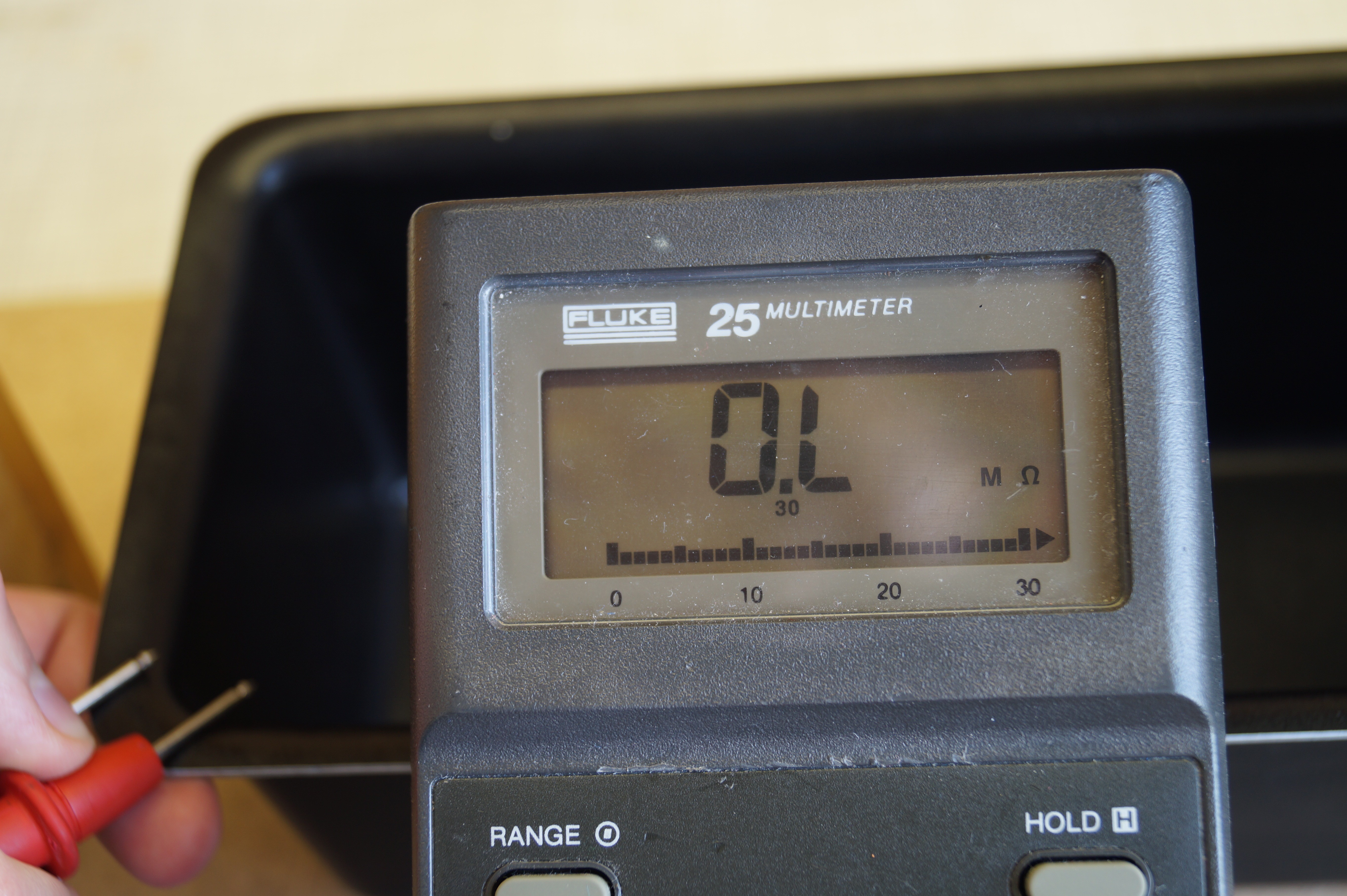
I am using a simple cake tin as a reservoir to hold the solution on which I will experiment. It is made of metal, but it has a coating which I have confirmed to be non-conductive.
![]()
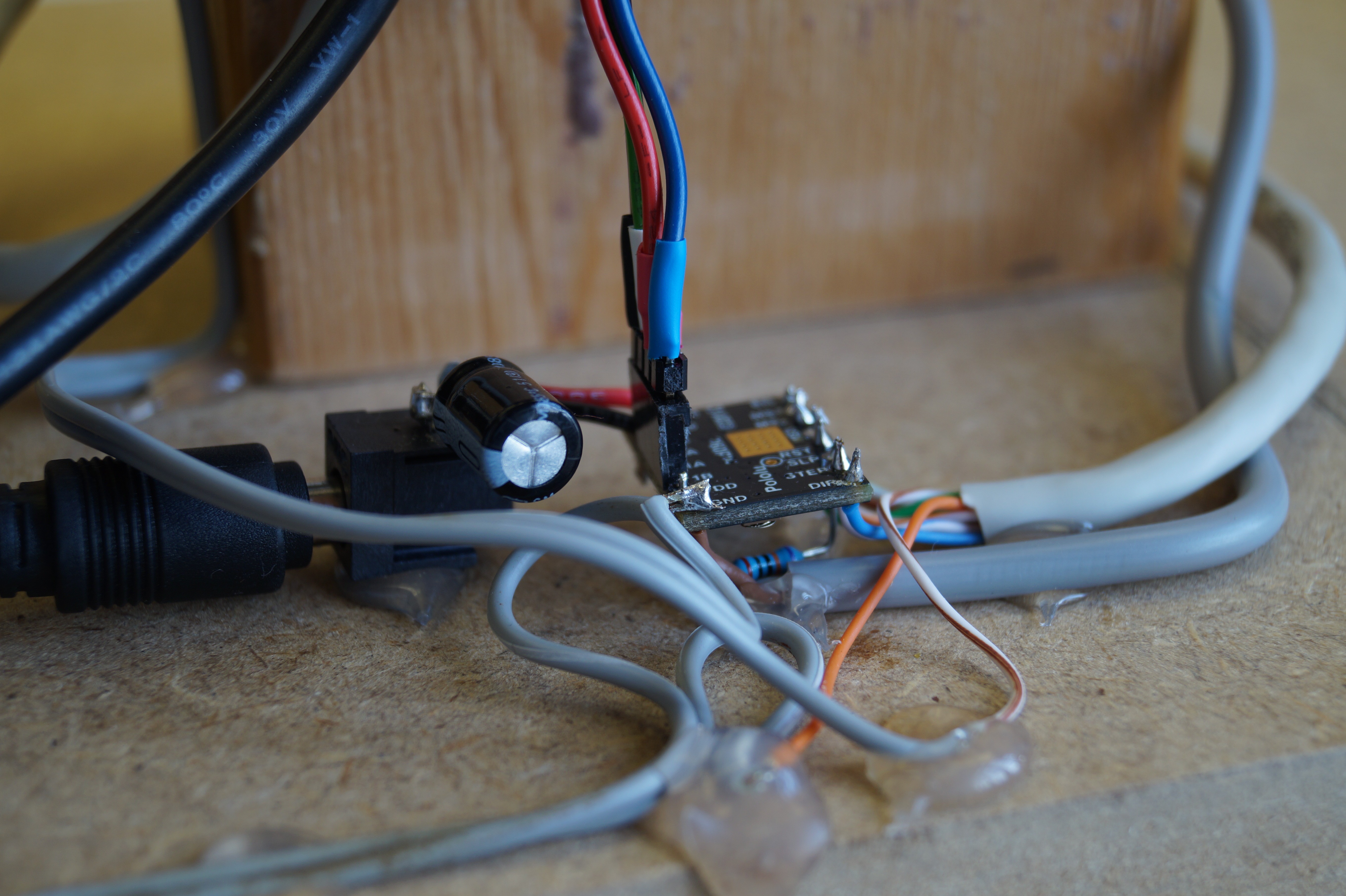
Additional electronics
![]()
To drive the stepper motor, a small driver board was needed, along with some limit switches to make sure the setup doesn't destroy itself. To connect to these and to the computer, some cables have to be run to RISA. I had already made a header for the stepper motor connections, but I forgot to include limit switch connections and the logic supply for the stepper motor driver. To fix this, I soldered a bodge wire to another point on the signal generator board and repurposed the I/O meant to go to the enable and sleep pins as inputs for the limit switches, since I really don't need to change the sleep mode of the stepper motor driver.
![]()
I used an ethernet cable and some two-conductor cable to route all the connections to the driver board, where some split of to the limit switches. I connected to those by another two-conductor cable.
![]()
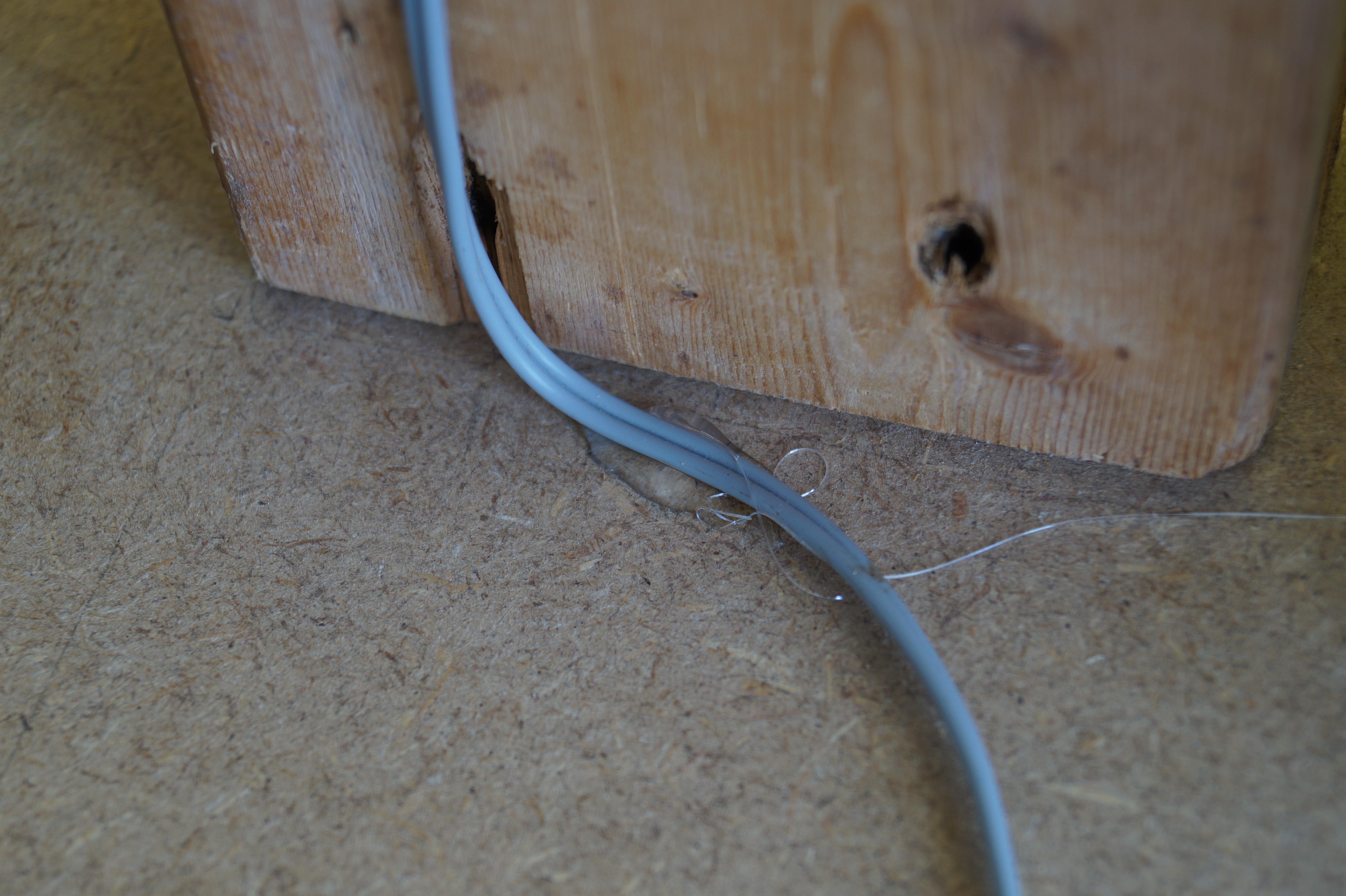
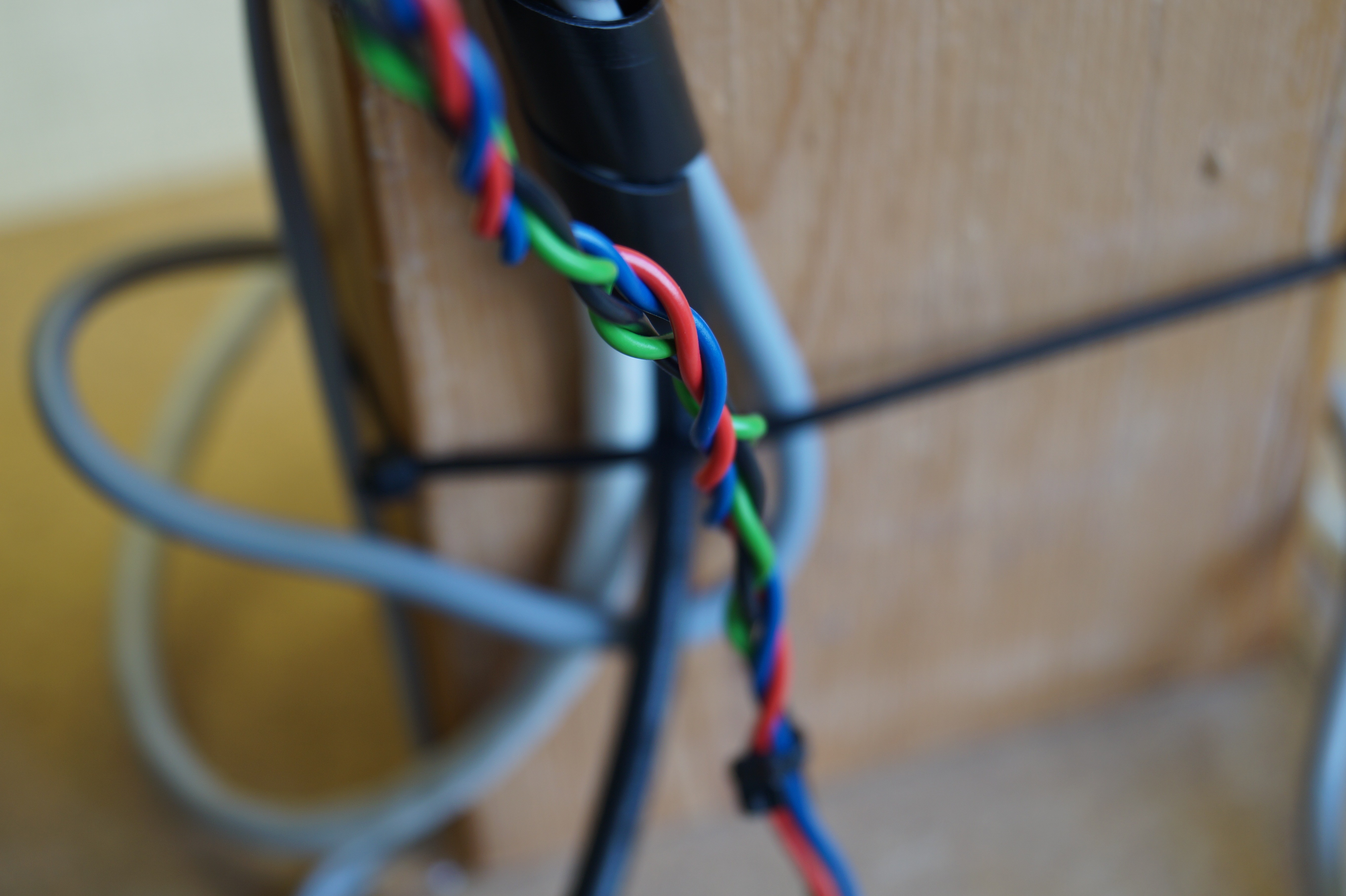
At this point, I had a lot of cables. That's all fine and dandy, but when the slider starts moving, I don't want any of them to get pulled, so cable management was needed. I stuck down the cables of the limit switches with hot glue.
![]()
The three cables coming of of RISA were fed through a cable guide, which was stuck down with cable ties.
![]()
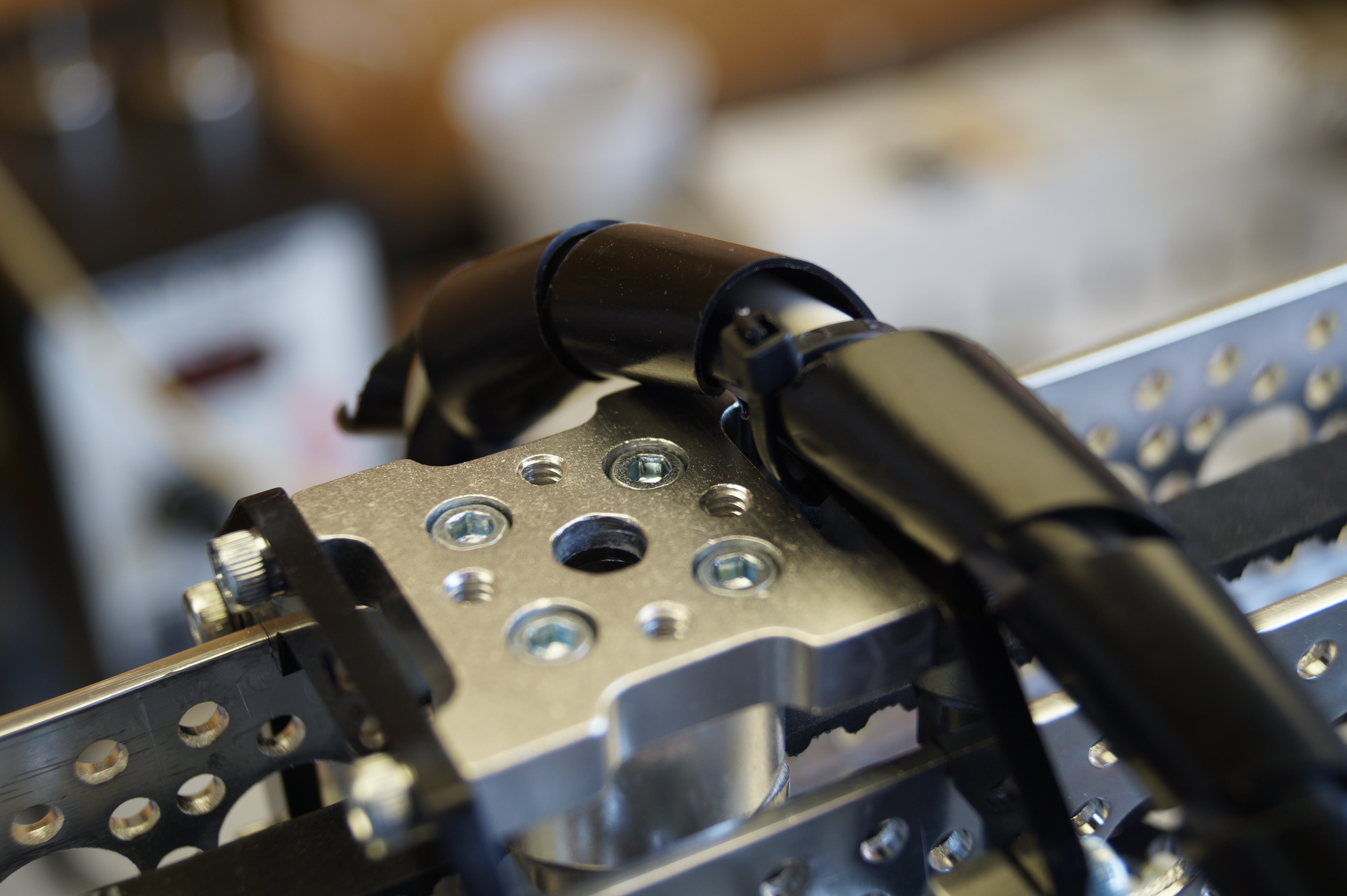
I also twisted the cables coming of of one coil of the stepper motor together, and than twisted those pairs again so that these cables would be held together. I put a tie rap on them to prevent them from untangling.
![]()
I think these simple things made the cabling quite neat.
Testing
After building the setup, I immediately tested whether the stepper motor turned. It did, but after reprogramming the Teensy it did not. When reprogramming the Teensy, the motor made a terrible buzzing sound, probably because the signals to program the Teensy are on the same lines as the stepper motor control pins.
I measured all signals going to the stepper driver, and even used my oscilloscope to examine the waveforms going to the stepper motor, but everything seemed fine. The stepper motor even heated up as normal and made a nice buzzing sound, which changed with the frequency of the pulses on the STEP of the stepper motor driver.
It was only then that I took a look at the axle of the stepper motor and saw that the grub screw of the shaft coupler had vibrated loose. After tightening it down, everything worked as normal. It hasn't come of since, but I may apply some loctite or something similar if it does.
![]()
This was a bit of a facepalm moment for me, but at least I won't make this error in the future.
Anyhow, now the mechanical part of the setup is working great!
![]()
It looks like all the hardware is up and running, so next up will be the programming.
-
Update: current project status
07/10/2016 at 18:04 • 0 commentsI figured I should give you an indication of where the project is roughly standing right now.
As of writing this log, the RISA electronics has been assembled, and the mechanical parts have been designed. Only basic software test have been written.
![]()
Figure 1: A partially build base.
I have even 3D-printed some prototypes of the parts, but I will have to print a new revision for the final project. The reason I haven't printed this revision yet, is that I needed to my laptop to write these logs, instead of it being tied to a printer. The slider and base have also been assembled.
![]()
Figure 2: A picture from the electronics build process.
The last few days, I have focussed on actually documenting the project a bit. Since I like to write quite extensively, this has meant that the documentation has sucked up all my time. I have now documented most of what was done until now, except for the build process however. This means that I will resume working on the core of the project next, and then document the new stuff as I finish it, with one exception: I have gathered quite a lot of images of the build process, so I will probably also start writing some of that.
Anyhow, those are the plans, I hope you'll enjoy the documentation of the project!
-
DAC with DMA and buffer on a Teensy 3.2
07/10/2016 at 14:12 • 2 commentsAlthough I haven't started programming the main program for RISA yet, I have done some tests. For one of them, I tried to get the DAC working. Since the main application will have to both read out two ADCs and write data to the DAC, I want to try to decouple as much as I can from the processor. Hence, I tried to get the DAC working with its internal buffer and Direct Memory Acces (DMA). I couldn't really found a tutorial on how to do this, so it took while. Because of that, I figured I would write up one of my own here.
If you don't know about DMA, it is a pretty cool feature, where microcontroller peripherals can automatically interact with the RAM to continue functioning while the processor can do other stuff. In addition, the DAC has a 16-word (16 times 2 bytes) buffer for storing values. By using this buffer the DMA can be used less frequently, allowing more time for other peripherals to acces it.
I have found really good examples of using the DAC with DMA without its buffer and of using the DAC with it's buffer, but without DMA, but nothing that combined those. After some reading of the datasheet, I now know how to do that. Still most of this tutorial was built on these examples, so a big thanks to pjrc forum users ferdinandkeil and the_pman for putting them up there.
I have made all register names hyperlinks their place in the datasheet, so if you want to see what they do, just click on them to read all about them. All example code is of the Teensyduino flavor, but if you need to adapt it to the Kinetis SDK, most of what you need to do is change minor differences in register names
This tutorial assumes basic familiarity with arduino, C, bitwise logic and pointers
The code
Initialising the DAC
We start by initialising the DAC itself. First, the clock to the DAC module will need to be enabled. This can be done by setting bit 12 of the System Clock Gating Control Register 2:
SIM_SCGC2 |= SIM_SCGC2_DAC0; // enable DAC clockThen we need to configure the DAC how we want it, that is to say: enabled and using VDDA as the voltage reference. To do this, we need to set the DAC enable and the DAC reference select bit in the DAC Control Register. The datasheet is a bit cryptic about the function of the DAC reference select bit, saying that it select between DACREF_1 and DACREF_2 as the voltage reference. Luckily, section 3.7.3.3 defines what both of those are: DACREF_1 is VREF_OUT and DACREF_2 is VDDA. Anyhow, to flip the bits we need to execute:
DAC0_C0 = DAC_C0_DACEN | DAC_C0_DACRFS; // enable the DAC module, 3.3V referenceThe DAC is now ready to use! Any 12-bit value you write to the address of the DAC Data Low Register will appear as an analog voltage between 0V and 3.3V on the DAC pin of the teensy. You may want to slowly ramp up the voltage of the DAC to avoid sharp edges on your signal:
  // slowly ramp up to DC voltage
  for (int16_t i=0; i<2048; i+=1) {
    *(int16_t *)&(DAC0_DAT0L) = i;
    delayMicroseconds(125);
  }
Now we fill the buffer with some constant values, so that there are no jumps in the output when we init the DAC buffer and the DAC first sweeps through it:
// fill up the buffer with 2048
for (int16_t i=0; i<16; i+=1) {
  *(int16_t *)(&DAC0_DAT0L + 2*i) = 2048;
}
That's the setup of the DAC we will do the DMA part of the DAC setup later, but for now, you should have:
void setup() {
  SIM_SCGC2 |= SIM_SCGC2_DAC0; // enable DAC clock
  DAC0_C0 = DAC_C0_DACEN | DAC_C0_DACRFS; // enable the DAC module, 3.3V reference
  // slowly ramp up to DC voltage
  for (int16_t i=0; i<2048; i+=1) {
    *(int16_t *)&(DAC0_DAT0L) = i;
    delayMicroseconds(125); // this function may be broken
  }
  // fill up the buffer with 2048
  for (int16_t i=0; i<16; i+=1) {
    *(int16_t *)(&DAC0_DAT0L + 2*i) = 2048;//256*(16-i) - 1;
  }
}

void loop() {
  // do nothing
}
Initialising the DMA
The DMA has quite an elaborate initialisation. It may be possible to rewrite the code to use the DMAChannel library, which could make it a lot cleaner. For now, I'm quite happy with this implementation. I mostly got the details from this manual of the manufacturer.
We first need to initialise the DMA peripheral and the DMA Multiplexer, which controls which peripheral has access to the RAM. As with the DAC, we first need to enable the clocks to both modules, by setting the appropriate bits in System Clock Gating Control Register 6 and 7:
SIM_SCGC6 |= SIM_SCGC6_DMAMUX; // enable DMA MUX clock
SIM_SCGC7 |= SIM_SCGC7_DMA;    // enable DMA clock
Now we need to pick a channel for DMA acces. There are a multitude of channels, so that DMA can be configured for multiple peripherals. We're only using the DAC for now, so let's use channel 0. We need to enable it and set to what DMA requests it will listen, which will be those of the DAC. We can set these properties in the Channel Configuration register of this channel:DMAMUX0_CHCFG0 |= DMAMUX_SOURCE_DAC0; //Select DAC as request source DMAMUX0_CHCFG0 |= DMAMUX_ENABLE; //Enable DMA channel 0Next, we need to make our DMA channel able to listen to requests. This is done by enabling it in the Enable Request Register:
DMA_ERQ = DMA_ERQ_ERQ0; // Enable requests on DMA channel 0For the next part, we're gonna need a buffer in the RAM which we'll use as the source of the values for the DAC. To initialise one, we have to add the following to the beginning of our code:#define BUFFER_SIZE 480 static volatile uint16_t sinetable[BUFFER_SIZE];Please note that BUFFER_SIZE can be any integer value larger than 16, but the higher it is the more samples you will have in your generated waveforms. It also helps to keep it as a proper divisor of your clock frequency, so that the frequency of your waveforms is a nice round number. For this example code to work, the buffer size needs to be an integer multiple of 8, for reasons that will become apparent later. I have named my buffer 'sinetable', but you can name it anything you want, it is just an array.
Let's also put something interesting in our buffer. I like to do this at the beginning of the setup() routine. I'm going to put a sine wave in it:
// fill up the sine table for(int i=0; i<BUFFER_SIZE; i++) { sinetable[i] = 2048+(int)(2048*sin(((float)i)*20.0*6.28318530717958647692/((float)BUFFER_SIZE))); }Your code should now look something like this:
#define BUFFER_SIZE 480 static volatile uint16_t sinetable[BUFFER_SIZE]; void setup() { // fill up the sine table for(int i=0; i<BUFFER_SIZE; i++) { sinetable[i] = 2048+(int)(2048*sin(((float)i)*20.0*6.28318530717958647692/((float)BUFFER_SIZE))); } // initialise the DAC SIM_SCGC2 |= SIM_SCGC2_DAC0; // enable DAC clock DAC0_C0 = DAC_C0_DACEN | DAC_C0_DACRFS; // enable the DAC module, 3.3V reference // slowly ramp up to DC voltage for (int16_t i=0; i<2048; i+=1) { *(int16_t *)&(DAC0_DAT0L) = i; delayMicroseconds(125); // this function may be broken } // fill up the buffer with 2048 for (int16_t i=0; i<16; i+=1) { *(int16_t *)(&DAC0_DAT0L + 2*i) = 2048;//256*(16-i) - 1; } // initialise the DMA // first, we need to init the dma and dma mux // to do this, we enable the clock to DMA and DMA MUX using the system timing registers SIM_SCGC6 |= SIM_SCGC6_DMAMUX; // enable DMA MUX clock SIM_SCGC7 |= SIM_SCGC7_DMA; // enable DMA clock // next up, the channel in the DMA MUX needs to be configured DMAMUX0_CHCFG0 |= DMAMUX_SOURCE_DAC0; //Select DAC as request source DMAMUX0_CHCFG0 |= DMAMUX_ENABLE; //Enable DMA channel 0 // then, we enable requests on our channel DMA_ERQ = DMA_ERQ_ERQ0; // Enable requests on DMA channel 0 } void loop() { // do nothing }Setting the Transfer Control Descriptor (TCD)
Back to where we were, we are now going to set the details of our DMA transfers. First, we choose where we want our data to come from, and were we want it to go, using the TCD Source and Destination Address register. Obviously, we want our data to come from our buffer, and go to the DAC buffer:
DMA_TCD0_SADDR = sinetable;   // set the address of the first byte in our LUT as the source address
DMA_TCD0_DADDR = &DAC0_DAT0L; // set the first data register as the destination address
You can transfer a maximum of 16 bytes in one cycle with the DMA, according to the datasheet. This would be great, since that is exactly 8 words, of half the buffer. We can only fill half the buffer at a time, since we can't both write to and read from the buffer at the same time. Since the DAC is always reading from one address in the buffer, we can't fill the full buffer in one go, we have to fill it in two writes. If we could fdo a write in one cycle, by having a transfer size of 16 bytes, we would have achieved the smallest tax on the DMA resources possible. For some reason, I haven't been able to use this transfer size unfortunately, so I will configure everything for the next-largest size, which is 32-bits, or 4 bytes.
First, we are going to set the read and write offset. This is the amount of bytes the read and write pointers respectively advance per read. Since we don't want to read or write data doubly, we set this to our transfer size of 4 bytes by configuring the TCD Signed Source and Destination Address Offset:
  DMA_TCD0_SOFF = 4; // advance 32 bits, or 4 bytes per read
  DMA_TCD0_DOFF = 4; // advance 32 bits, or 4 bytes per write
Now we get to set the actual transfer size. We can also set up a modulo, which controls the amount of the least significant bits that may change before resetting to the initial source or destination address. We are going to set this up for the DAC buffer, since it starts at a address that ends in zeroes and its size is a power of two. We do both things by setting up the TCD Transfer Attributes register:DMA_TCD0_ATTR = DMA_TCD_ATTR_SSIZE(DMA_TCD_ATTR_SIZE_32BIT); DMA_TCD0_ATTR |= DMA_TCD_ATTR_DSIZE(DMA_TCD_ATTR_SIZE_32BIT) | DMA_TCD_ATTR_DMOD(31 - __builtin_clz(32)); // set the data transfer size to 32 bit for both the source and the destinationThe data sheet has some terminology that I found a bit confusing on my first readthrough. Every request is considered a 'minor loop'. It is a loop, since we can set multiple transfers to be executed, which the hardware will presumably loop through. 'Major loops' can also be configured. You can set the number of minor loops that fit in a major loop. Basically, every time this number of minor loops, or requests, has completed, the major loop start over. The DMA can be configured so that at the end of the major loop, the source and destination address are changed. I think it helps to think of the minor loops as sort of a request counter, and the major loop as an oppurtunity to change the source and destination address.
We will use this oppurtunity to reset the source address back to the start of the buffer, since we can't use the modulo function for our buffer, as it is not aligned to an adress ending in zeroes and its size isn't a power of two. This does mean that an integer number of minor loops has to fit in our buffer, which is why its size had to be an integer multiple of 8.
Anyhow, we want to fill half our buffer every minor loop, which is 8 words, or 16 bytes. We can set the number of bytes we want to transfer per minor loop in the TCD Minor Byte Count (Minor Loop Disabled) register[1]:
DMA_TCD0_NBYTES_MLNO = 16; // we want to fill half of the DAC buffer, which is 16 words in total, so we need 8 words - or 16 bytes - per transferNow we need to set the number of minor loops in a major loop, or the number of requests before we reset to the original source address. To do this, we must set the current major iteration counter in the TCD Current Minor Loop Link, Major Loop Count (ChannelLinking Disabled) register and the value to which it will be reset when the major loop completes in the TCD Beginning Minor Loop Link, Major Loop Count (ChannelLinking Disabled) register:
// set the number of minor loops (requests) in a major loop
DMA_TCD0_CITER_ELINKNO = DMA_TCD_CITER_ELINKYES_CITER(BUFFER_SIZE*2/16);
DMA_TCD0_BITER_ELINKNO = DMA_TCD_BITER_ELINKYES_BITER(BUFFER_SIZE*2/16);
Then we need to set the amount we want to change the source and destination adress when the major loop completes in bytes. We only need to adjust the source address, since the destination adress is handled by the modulo we set up. We need to set back the source address by double the buffer size, since our buffer is made up of integers, which are 2 bytes. We can do this by setting adjustments in the TCD Last Source Address Adjustment registerTCD Last Source Address Adjustment register and the TCD Last Destination Address Adjustment/Scatter GatherAddress register:
  DMA_TCD0_SLAST    = -BUFFER_SIZE*2;
  DMA_TCD0_DLASTSGA = 0;
The only thing left for us to do is to initialise the TCD Control and Status register:
DMA_TCD0_CSR = 0;Your code should now look like this:
#define BUFFER_SIZE 480
static volatile uint16_t sinetable[BUFFER_SIZE];
void setup() {
  // fill up the sine table
  for(int i=0; i<BUFFER_SIZE; i++) {
    sinetable[i] = 2048+(int)(2048*sin(((float)i)*20.0*6.28318530717958647692/((float)BUFFER_SIZE)));
  }
  // initialise the DAC
  SIM_SCGC2 |= SIM_SCGC2_DAC0; // enable DAC clock
  DAC0_C0 = DAC_C0_DACEN | DAC_C0_DACRFS; // enable the DAC module, 3.3V reference
  // slowly ramp up to DC voltage
  for (int16_t i=0; i<2048; i+=1) {
    *(int16_t *)&(DAC0_DAT0L) = i;
    delayMicroseconds(125); // this function may be broken
  }
  // fill up the buffer with 2048
  for (int16_t i=0; i<16; i+=1) {
    *(int16_t *)(&DAC0_DAT0L + 2*i) = 2048;//256*(16-i) - 1;
  }
  // initialise the DMA
  // first, we need to init the dma and dma mux
  // to do this, we enable the clock to DMA and DMA MUX using the system timing registers
  SIM_SCGC6 |= SIM_SCGC6_DMAMUX; // enable DMA MUX clock
  SIM_SCGC7 |= SIM_SCGC7_DMA;    // enable DMA clock
  // next up, the channel in the DMA MUX needs to be configured
  DMAMUX0_CHCFG0 |= DMAMUX_SOURCE_DAC0; //Select DAC as request source
  DMAMUX0_CHCFG0 |= DMAMUX_ENABLE;      //Enable DMA channel 0
  // then, we enable requests on our channel
  DMA_ERQ = DMA_ERQ_ERQ0; // Enable requests on DMA channel 0
  // Here we choose where our data is coming from, and where it is going
  DMA_TCD0_SADDR = sinetable;   // set the address of the first byte in our LUT as the source address
  DMA_TCD0_DADDR = &DAC0_DAT0L; // set the first data register as the destination address
  // now we need to set the read and write offsets - kind of boring
  DMA_TCD0_SOFF = 4; // advance 32 bits, or 4 bytes per read
  DMA_TCD0_DOFF = 4; // advance 32 bits, or 4 bytes per write
  // this is the fun part! Now we get to set the data transfer size...
  DMA_TCD0_ATTR  = DMA_TCD_ATTR_SSIZE(DMA_TCD_ATTR_SIZE_32BIT);
  DMA_TCD0_ATTR |= DMA_TCD_ATTR_DSIZE(DMA_TCD_ATTR_SIZE_32BIT) | DMA_TCD_ATTR_DMOD(31 - __builtin_clz(32)); // set the data transfer size to 32 bit for both the source and the destination
  // ...and the number of bytes to be transferred per request (or 'minor loop')...
  DMA_TCD0_NBYTES_MLNO = 16; // we want to fill half of the DAC buffer, which is 16 words in total, so we need 8 words - or 16 bytes - per transfer
  // set the number of minor loops (requests) in a major loop
  // the circularity of the buffer is handled by the modulus functionality in the TCD attributes
  DMA_TCD0_CITER_ELINKNO = DMA_TCD_CITER_ELINKYES_CITER(BUFFER_SIZE*2/16);
  DMA_TCD0_BITER_ELINKNO = DMA_TCD_BITER_ELINKYES_BITER(BUFFER_SIZE*2/16);
  // the address is adjusted by these values when a major loop completes
  // we don't need this for the destination, because the circularity of the buffer is already handled
  DMA_TCD0_SLAST    = -BUFFER_SIZE*2;
  DMA_TCD0_DLASTSGA = 0;
  // do the final init of the channel
  DMA_TCD0_CSR = 0;
}
void loop() {
  // do nothing
}
Setting up the DAC for buffered DMA
Now it's time to set up the DMA of the DAC. There are three interrupts that the DAC can generate, which are used in the DAC buffer example. These are:
- The DAC Buffer Read Pointer Top Flag Interrupt, which interrupts when the read pointer of the DAC Buffer is 0.
- The DAC Buffer Read Pointer Bottom Flag Interrupt, which interrupts when the read pointer of the Dac Buffer has reached the last word of the buffer.
- The DAC Buffer Watermark Interrupt, which interrupts when the read pointer is the amount in DAC Buffer Watermark Select away from the last word.
Instead of interrupts, the DAC can be set up to generate DMA requests. We will be doing exactly this. First, we must enable two interrupts, the watermark and another one. I found that sometimes, I could fix glitches in the generated signal by choosing another interrupt. For this example, the read pointer bottom flag interrupt works great. We can enable the interupts using the DAC Control Register:
DAC0_C0 |= DAC_C0_DACBBIEN | DAC_C0_DACBWIEN; // enable read pointer bottom and waterwark interruptThen, we can generate DMA request instead of interrupts, enable the DAC buffer and set the correct watermark offset by writing to the DAC Control Register 1:
DAC0_C1 |= DAC_C1_DMAEN | DAC_C1_DACBFEN | DAC_C1_DACBFWM(3); // enable dma and bufferLastly, we can set the inital position of the read pointer. Again, I found that I could sometimes fix glitches in the signal by setting the read pointer to a position beyond a certain interrupt, which probalby worked because in this alternate interrupt order the DMA had more time to catch up to the DAC requests. We can change the pointer position by changing the DAC Control Register 2:
DAC0_C2 |= DAC_C2_DACBFRP(0);By this point, you code should look like this:#define BUFFER_SIZE 480 static volatile uint16_t sinetable[BUFFER_SIZE]; void setup() { // fill up the sine table for(int i=0; i<BUFFER_SIZE; i++) { sinetable[i] = 2048+(int)(2048*sin(((float)i)*20.0*6.28318530717958647692/((float)BUFFER_SIZE))); } // initialise the DAC SIM_SCGC2 |= SIM_SCGC2_DAC0; // enable DAC clock DAC0_C0 = DAC_C0_DACEN | DAC_C0_DACRFS; // enable the DAC module, 3.3V reference // slowly ramp up to DC voltage for (int16_t i=0; i<2048; i+=1) { *(int16_t *)&(DAC0_DAT0L) = i; delayMicroseconds(125); // this function may be broken } // fill up the buffer with 2048 for (int16_t i=0; i<16; i+=1) { *(int16_t *)(&DAC0_DAT0L + 2*i) = 2048;//256*(16-i) - 1; } // initialise the DMA // first, we need to init the dma and dma mux // to do this, we enable the clock to DMA and DMA MUX using the system timing registers SIM_SCGC6 |= SIM_SCGC6_DMAMUX; // enable DMA MUX clock SIM_SCGC7 |= SIM_SCGC7_DMA; // enable DMA clock // next up, the channel in the DMA MUX needs to be configured DMAMUX0_CHCFG0 |= DMAMUX_SOURCE_DAC0; //Select DAC as request source DMAMUX0_CHCFG0 |= DMAMUX_ENABLE; //Enable DMA channel 0 // then, we enable requests on our channel DMA_ERQ = DMA_ERQ_ERQ0; // Enable requests on DMA channel 0 // first, we need to init the dma and dma mux // to do this, we enable the clock to DMA and DMA MUX using the system timing registers SIM_SCGC6 |= SIM_SCGC6_DMAMUX; // enable DMA MUX clock SIM_SCGC7 |= SIM_SCGC7_DMA; // enable DMA clock // next up, the channel in the DMA MUX needs to be configured DMAMUX0_CHCFG0 |= DMAMUX_SOURCE_DAC0; //Select DAC as request source DMAMUX0_CHCFG0 |= DMAMUX_ENABLE; //Enable DMA channel 0 // then, we enable requests on our channel DMA_ERQ = DMA_ERQ_ERQ0; // Enable requests on DMA channel 0 // Here we choose where our data is coming from, and where it is going DMA_TCD0_SADDR = sinetable; // set the address of the first byte in our LUT as the source address DMA_TCD0_DADDR = &DAC0_DAT0L; // set the first data register as the destination address // now we need to set the read and write offsets - kind of boring DMA_TCD0_SOFF = 4; // advance 32 bits, or 4 bytes per read DMA_TCD0_DOFF = 4; // advance 32 bits, or 4 bytes per write // this is the fun part! Now we get to set the data transfer size... DMA_TCD0_ATTR = DMA_TCD_ATTR_SSIZE(DMA_TCD_ATTR_SIZE_32BIT); DMA_TCD0_ATTR |= DMA_TCD_ATTR_DSIZE(DMA_TCD_ATTR_SIZE_32BIT) | DMA_TCD_ATTR_DMOD(31 - __builtin_clz(32)); // set the data transfer size to 32 bit for both the source and the destination // ...and the number of bytes to be transferred per request (or 'minor loop')... DMA_TCD0_NBYTES_MLNO = 16; // we want to fill half of the DAC buffer, which is 16 words in total, so we need 8 words - or 16 bytes - per transfer // set the number of minor loops (requests) in a major loop // the circularity of the buffer is handled by the modulus functionality in the TCD attributes DMA_TCD0_CITER_ELINKNO = DMA_TCD_CITER_ELINKYES_CITER(BUFFER_SIZE*2/16); DMA_TCD0_BITER_ELINKNO = DMA_TCD_BITER_ELINKYES_BITER(BUFFER_SIZE*2/16); // the address is adjusted by these values when a major loop completes // we don't need this for the destination, because the circularity of the buffer is already handled DMA_TCD0_SLAST = -BUFFER_SIZE*2; DMA_TCD0_DLASTSGA = 0; // do the final init of the channel DMA_TCD0_CSR = 0; // enable DAC DMA DAC0_C0 |= DAC_C0_DACBBIEN | DAC_C0_DACBWIEN; // enable read pointer bottom and waterwark interrupt DAC0_C1 |= DAC_C1_DMAEN | DAC_C1_DACBFEN | DAC_C1_DACBFWM(3); // enable dma and buffer DAC0_C2 |= DAC_C2_DACBFRP(0); } void loop() { // do nothing }Setting up the DAC interval
While the DAC itself has a clock, that doesn't advance the DAC buffer pointer. To do that, we need to set up a Programmable Delay Block to generate the DAC intervals. As before, we first need to enable the clock to the PDB using the System Clock Gating Control Register 6:
SIM_SCGC6 |= SIM_SCGC6_PDB; // turn on the PDB clockNow, we need to enable the PDB, select the software trigger as trigger source and select the continuous run mode. This can all be set up in the PDB Status and Control register:
PDB0_SC |= PDB_SC_PDBEN; // enable the PDB
PDB0_SC |= PDB_SC_TRGSEL(15); // trigger the PDB on software start (SWTRIG)
PDB0_SC |= PDB_SC_CONT; // run in continuous mode
Now we need to set the amount of cycles in a PDB period, the modulus time. This is set in the PDB Modulus register:PDB0_MOD = 20-1; // modulus time for the PDBYou shouldn't go lower than this value. I have set it at it lowest, to achieve the maximum sample rate possible. If you go any lower, the DMA can't keep up with the DAC, and you get a glitchy signal. A way to attain an even higher sample rate would be to make the transfer take less time, which you can accomplish by having a transfer size of 16 bytes. This way, the sample rate could probably be increased by a factor of 4 If you want lower frequencies, you should change the amount of sines in the buffer, or enlarge the buffer.
Next, we set the amount of cycles in the actual DAC interval. By having this be equal to the modulus time, the period will be the same as the PDB period. It can be set in the DAC Interval Register:
PDB0_DACINT0 = (uint16_t)(20-1); // we won't subdivide the clock
Then, we need to enable the DAC interval trigger, by setting the DAC Interval Trigger Control Register:PDB0_DACINTC0 |= 0x01; // enable the DAC interval trigger
To update all the PDB registers, the Load OK bit needs to be set to 1 in the PDB Status and Control register:PDB0_SC |= PDB_SC_LDOK; // update pdb registers
Finally, we can start this complicated beast by one simple software trigger, written to the PDB Status and Control register:PDB0_SC |= PDB_SC_SWTRIG;
At this point, your completed code should resemble this:#define BUFFER_SIZE 480 static volatile uint16_t sinetable[BUFFER_SIZE]; void setup() { // fill up the sine table for(int i=0; i<BUFFER_SIZE; i++) { sinetable[i] = 2048+(int)(2048*sin(((float)i)*20.0*6.28318530717958647692/((float)BUFFER_SIZE))); } // initialise the DAC SIM_SCGC2 |= SIM_SCGC2_DAC0; // enable DAC clock DAC0_C0 = DAC_C0_DACEN | DAC_C0_DACRFS; // enable the DAC module, 3.3V reference // slowly ramp up to DC voltage for (int16_t i=0; i<2048; i+=1) { *(int16_t *)&(DAC0_DAT0L) = i; delayMicroseconds(125); // this function may be broken } // fill up the buffer with 2048 for (int16_t i=0; i<16; i+=1) { *(int16_t *)(&DAC0_DAT0L + 2*i) = 2048;//256*(16-i) - 1; } // initialise the DMA // first, we need to init the dma and dma mux // to do this, we enable the clock to DMA and DMA MUX using the system timing registers SIM_SCGC6 |= SIM_SCGC6_DMAMUX; // enable DMA MUX clock SIM_SCGC7 |= SIM_SCGC7_DMA; // enable DMA clock // next up, the channel in the DMA MUX needs to be configured DMAMUX0_CHCFG0 |= DMAMUX_SOURCE_DAC0; //Select DAC as request source DMAMUX0_CHCFG0 |= DMAMUX_ENABLE; //Enable DMA channel 0 // then, we enable requests on our channel DMA_ERQ = DMA_ERQ_ERQ0; // Enable requests on DMA channel 0 // first, we need to init the dma and dma mux // to do this, we enable the clock to DMA and DMA MUX using the system timing registers SIM_SCGC6 |= SIM_SCGC6_DMAMUX; // enable DMA MUX clock SIM_SCGC7 |= SIM_SCGC7_DMA; // enable DMA clock // next up, the channel in the DMA MUX needs to be configured DMAMUX0_CHCFG0 |= DMAMUX_SOURCE_DAC0; //Select DAC as request source DMAMUX0_CHCFG0 |= DMAMUX_ENABLE; //Enable DMA channel 0 // then, we enable requests on our channel DMA_ERQ = DMA_ERQ_ERQ0; // Enable requests on DMA channel 0 // Here we choose where our data is coming from, and where it is going DMA_TCD0_SADDR = sinetable; // set the address of the first byte in our LUT as the source address DMA_TCD0_DADDR = &DAC0_DAT0L; // set the first data register as the destination address // now we need to set the read and write offsets - kind of boring DMA_TCD0_SOFF = 4; // advance 32 bits, or 4 bytes per read DMA_TCD0_DOFF = 4; // advance 32 bits, or 4 bytes per write // this is the fun part! Now we get to set the data transfer size... DMA_TCD0_ATTR = DMA_TCD_ATTR_SSIZE(DMA_TCD_ATTR_SIZE_32BIT); DMA_TCD0_ATTR |= DMA_TCD_ATTR_DSIZE(DMA_TCD_ATTR_SIZE_32BIT) | DMA_TCD_ATTR_DMOD(31 - __builtin_clz(32)); // set the data transfer size to 32 bit for both the source and the destination // ...and the number of bytes to be transferred per request (or 'minor loop')... DMA_TCD0_NBYTES_MLNO = 16; // we want to fill half of the DAC buffer, which is 16 words in total, so we need 8 words - or 16 bytes - per transfer // set the number of minor loops (requests) in a major loop // the circularity of the buffer is handled by the modulus functionality in the TCD attributes DMA_TCD0_CITER_ELINKNO = DMA_TCD_CITER_ELINKYES_CITER(BUFFER_SIZE*2/16); DMA_TCD0_BITER_ELINKNO = DMA_TCD_BITER_ELINKYES_BITER(BUFFER_SIZE*2/16); // the address is adjusted by these values when a major loop completes // we don't need this for the destination, because the circularity of the buffer is already handled DMA_TCD0_SLAST = -BUFFER_SIZE*2; DMA_TCD0_DLASTSGA = 0; // do the final init of the channel DMA_TCD0_CSR = 0; // enable DAC DMA DAC0_C0 |= DAC_C0_DACBBIEN | DAC_C0_DACBWIEN; // enable read pointer bottom and waterwark interrupt DAC0_C1 |= DAC_C1_DMAEN | DAC_C1_DACBFEN | DAC_C1_DACBFWM(3); // enable dma and buffer DAC0_C2 |= DAC_C2_DACBFRP(0); // init the PDB for DAC interval generation SIM_SCGC6 |= SIM_SCGC6_PDB; // turn on the PDB clock PDB0_SC |= PDB_SC_PDBEN; // enable the PDB PDB0_SC |= PDB_SC_TRGSEL(15); // trigger the PDB on software start (SWTRIG) PDB0_SC |= PDB_SC_CONT; // run in continuous mode PDB0_MOD = 20-1; // modulus time for the PDB PDB0_DACINT0 = (uint16_t)(20-1); // we won't subdivide the clock... PDB0_DACINTC0 |= 0x01; // enable the DAC interval trigger PDB0_SC |= PDB_SC_LDOK; // update pdb registers PDB0_SC |= PDB_SC_SWTRIG; // ...and start the PDB } void loop() { // do nothing }Conclusion
So, now you know how to get DMA up and running with both DMA and the DAC buffer. Hopefully you also learnt something about programming or about the architecture of the Kinetis K20 (the family of ICs used in the teensy).
If you have any suggestions for improvements, or errors to point out, I would be happy to hear them.
Endnotes
[1] I guess I am not even using the minor loops. However, there does not seem to be much of a difference in operation, except that you can also use the minor loops to do some offsetting. My problems with getting the 16-byte transfer to work may originate in my misunderstanding of this mechanism. Of course, any suggestions are welcome, as always.
-
Electronics details
07/08/2016 at 13:01 • 0 commentsfoIn this log, let's examine the electronics of the Rapid Impedance Spectroscopy Array, RISA.
Construction
Figure 1: Unpopulated PCBs showing board stackup.![]()
RISA consists of 2 two-layer boards, which are connected by .1" headers. The reason for having two boards is that the electrode board couldn't have any solder joints on the bottom, because those could influence the flow and provide a path for current to flow to other than the electrode pads. Since I wanted all signal generation hardware to be through-hole for easy experimentation, I needed a separate PCB for that.
The electrode PCB (the bottom PCB in figure 1) contains 64 electrode pads at the backside, arranged in an 8 by 8 grid. On the topside, there are 4 4067 multiplexer IC's. These had to be surface mount to fit them on, and to not violate the no solder joint on bottom rule.
The signal generator PCB (the top PCB in figure 1) contains some analog electronics and some headers, in which a Teensy 3.2 is mounted, which does all the signal generation, measurement and contains the smarts of this project.
I will go into more detail about how this is mounted in the log about the mechanical side of the project, and the construction process can be found in the build instructions section in due time.
What it does
I have been mentioning Electrochemical Impedance Spectroscopy a lot, but what is it exactly?
Simply put, EIS is a technique where you measure the impedance of a sample over a certain frequency range. This data, called an impedance spectrum, can then be used in a number of ways. It can either be used to characterise electrical systems, such as filters, but it also has applications to find the chemical composition of a sample. EIS is used as a non-intrusive way to measure fat content in people's legs for example.
But what is impedance? For this project you only need to know a few things about it:
- Impedance is basically resistance that changes with frequency.
- Impedance has 2 parts to it:
- An imaginary part
- A real part
This is a gross simplification. I recommend watching this video for getting a more thorough understanding of the concept.
At its core, RISA switches two electrodes in its array to an AC signal output and ground, and measures the resulting current. It then repeats this process for various frequencies to obtain an impedance spectrum. It also has control over the stepper motor driving the linear slider on which it is mounted, so that it can influence the flow speed and gather impedance spectra for various amounts of flow.
How it does it
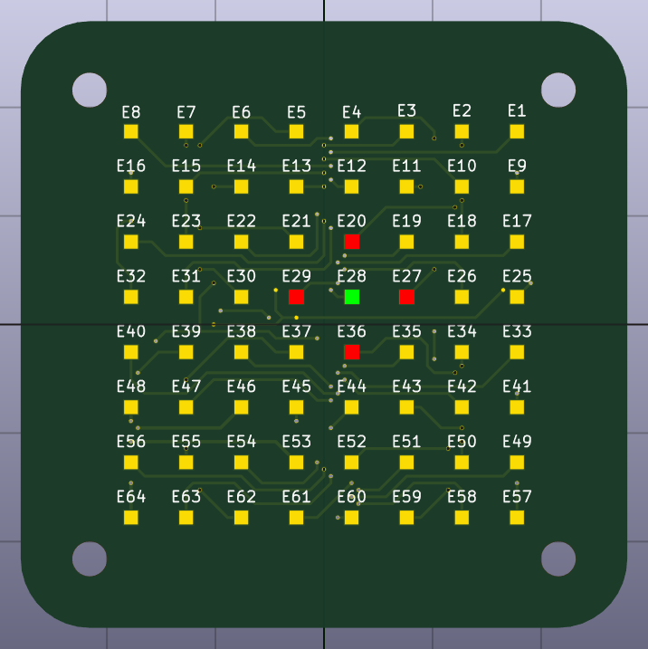
The array
RISA will only ever need to collect impedance spectra between adjacent electrodes, and only horizontally or vertically. So when electrode that I've highlighted green in figure 2 is in use, the only other electrodes that can be used are the ones that I've highlighted red.
![]()
Figure 2: The adjacent electrodes.
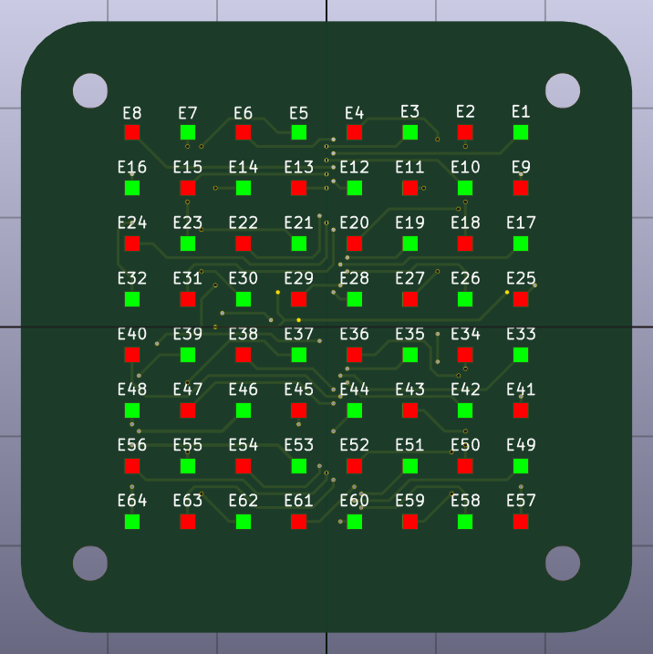
So we don't need two grids covering all electrodes, we just need a chess-board pattern:
![]()
Figure 3: The two electrode selection grids.
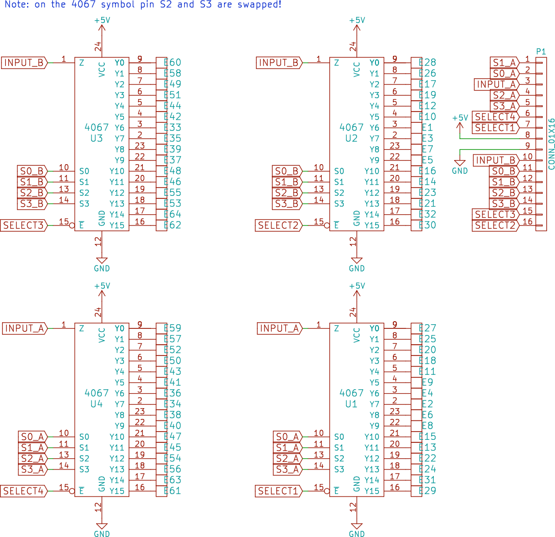
We then need electronics to select any electrode on both of those grids:
![]()
Figure 4: Electrode schematic.
For this, we use multiplexer ICs. If you're not familiar with those, they basically allow you to bidirectionally connect one or more inputs to one or more outputs. These IC's, the 4067, let you connect one input to 16 outputs. The S0 through S3 pins allow us to select which one, using a binary scheme. Using 2 of these, we can hook up every electrode in one of the grids to an input. But we still need to switch one of the 4067s off so that the input isn't connected to two electrodes. That is what the SELECT lines are for. Add another two, and we can connect every electrode in both grids to two inputs. These go off to the signal generator board, along with the digital lines used for selecting the right electrodes, via connector P1.
The signal generation
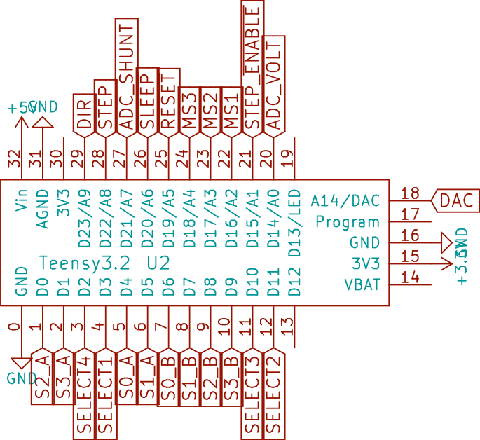
![]()
Figure 5: The Teensy 3.2 on the signal generator board schematic.
The signal generator board houses a Teensy 3.2. Almost all I/O of the Teensy are used. Some are used to switch to the right electrode, others to drive the stepper motor and others yet again for the analog signal generation and measurement.
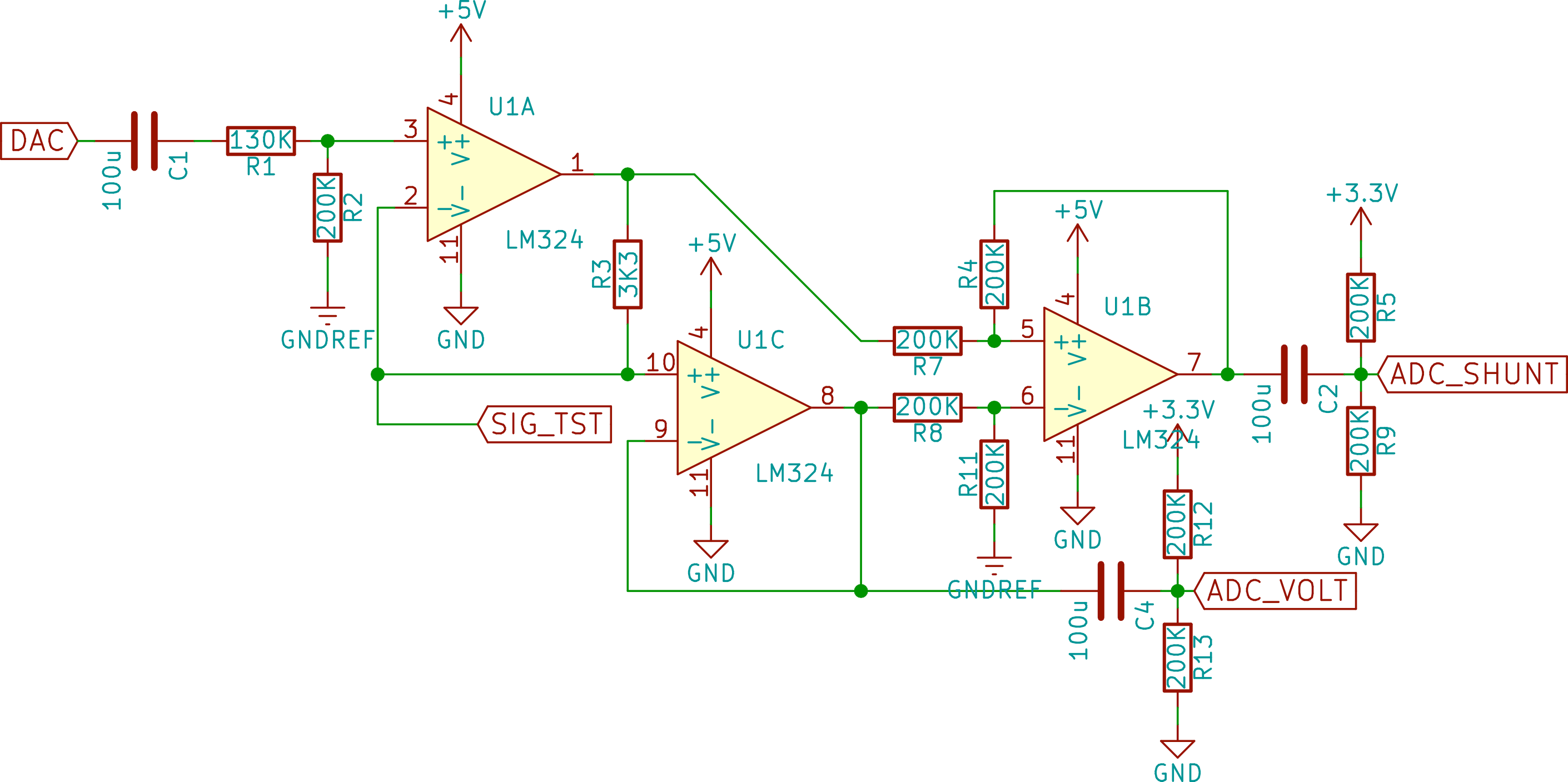
The Teensy 3.2 has a 12-bit DAC capable of generating all sorts of waveforms. There is one problem however: it generates signals from rail-to-rail, or from 0V to 3.3V. This is an issue because we need an alternating voltage that goes both above and below ground. Furthermore, we don't want it to be this high, to prevent electrolysis in the electrolytic solution.
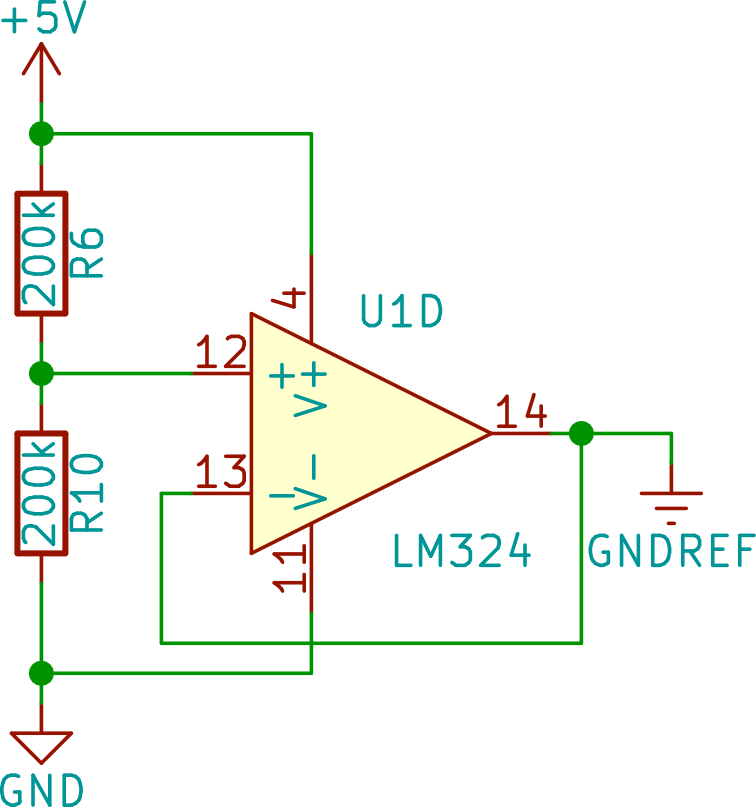
We can fix this problem by using some basic op-amp circuits. Instead of using the ground of our teensy as the ground reference for measurements, we can create what is called a virtual ground.
![]()
Figure 6: The operational amplifier circuit for creating a virtual ground.
This is done by simply dividing our supply voltage in half using a voltage divider, and buffering it with an opamp voltage follower circuit, so that the virtual ground is referenced by the current drawn from it. If we use this virtual ground, denoted by GNDREF in the schematic, we can obtain negative voltages relative to it, by just dipping below 2.5V, half the supply voltage. Our signal is yet centred nicely around this virtual ground however, and is still a bit to high.
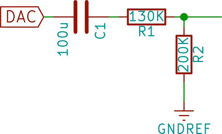
We can fix this by adding a high pass filter and voltage divider:
![]()
Figure 7: DAC Biasing and voltage scaling.
This works because the capacitor slowly charges up through the resistors to GNDREF, but allows our fast-changing measurement signal to pass through mostly unscathed. The signal is then divided down by R1 and R2 to 2V pk-pk.
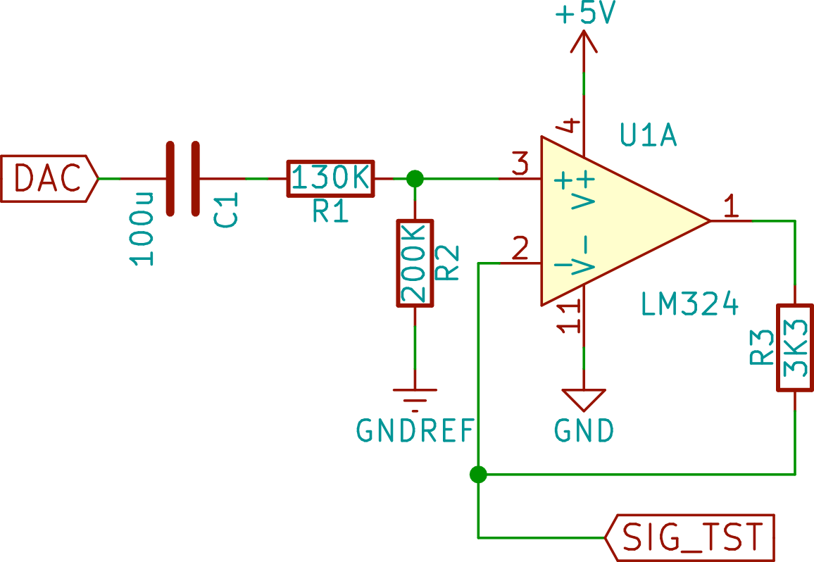
However, if I were to even draw I tiny current from here, the voltage would drop dramatically, due to the high resistance. Also, how do we go about measuring the current? We can use another op-amp circuit to accomplish these goals:
![]()
Figure 8: Signal buffering.
U1A Buffers the signal, like we did for the virtual ground. However, you may have noticed R3 in the feedback path. The larger the current being drawn by the solution, out of SIG_TST, the higher the voltage drop over R3 will be. Thus, we can use this drop to determine the current. The test signal doesn't drop because of this, since the op-amp will compensate for the drop since its negative input is connected after R3.
So that is our signal generation complete, but how do we go about measuring the current?
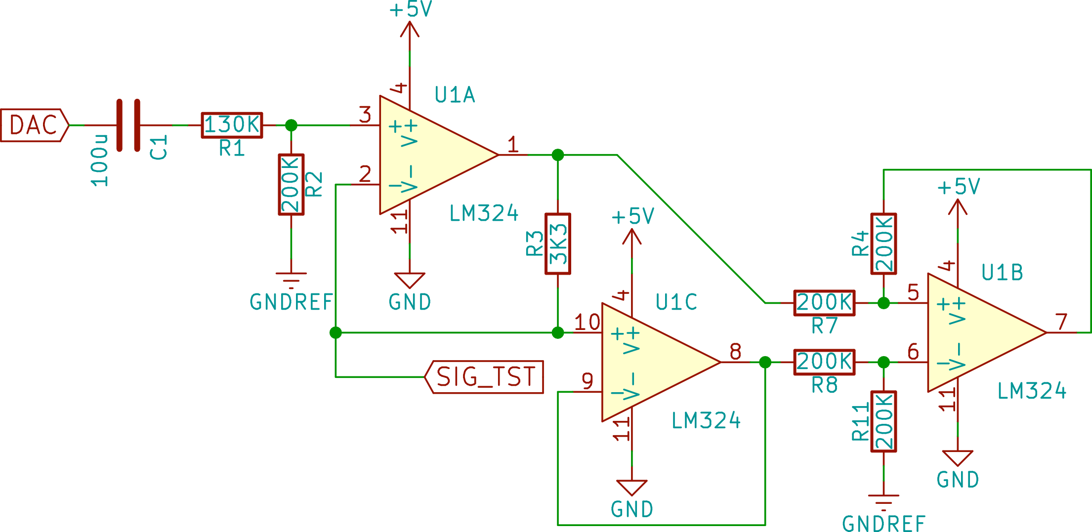
![]()
Figure 9: Buffered differential amplifier for current measurement.
That's right: more opamps. We can use a differential amplifier circuit (opamp U1B) to find the voltage over the resistor. We use GNDREF instead of the normal GND for the negative input to make sure negative currents can also be output. We buffer the test signal with U1C, since even the tiny amount of current that is drawn by the resistors connected to the negative input of U1B of about 5 uA is a significant impact on our measurement. Also, since opamp tend to come in either single, dual or quadruple packages, we would have had this opamp leftover anyway, so this is a good place to put it to use. The signal going to the positive input of the differential amplifier doesn't need any buffering, since it comes straight out of U1A, which has a low source resistance.
There is still one problem left: the signal put out by U1B is centred around GNDREF, 2.5V, while our ADC measures until 3.3V. To utilise the maximum dynamic range of the ADC, we need to bias the signal again. Also, since the Teensy 3.2 has two ADCs, why not use the second one to check on our test signal by tapping off the output of U1C. The completed circuit then looks like:
Figure 10: Completed signal generation and measurement circuit.![]()
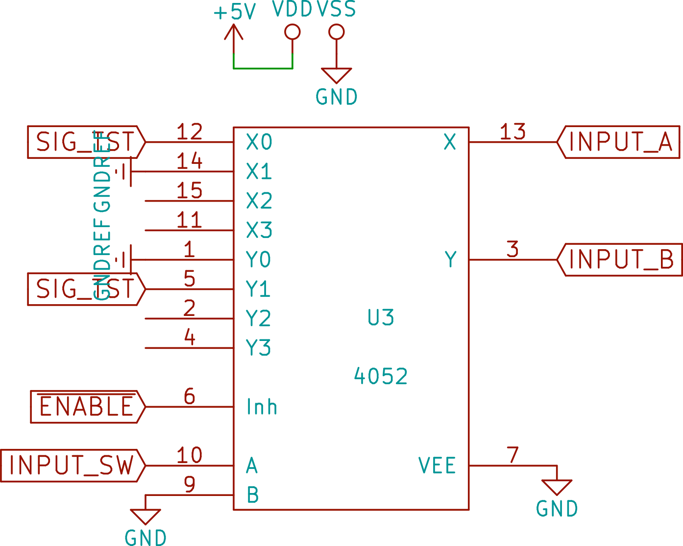
However, there is still more to talk about. I want to be able to obtain an impedance spectrum in both directions. To do this, you just need to add another switcher to the circuit:
Figure 11: Multiplexer for switching signal direction.![]()
This chip has way more inputs than needed, but by connecting switch input B to ground, we only select between X0 & Y0 and X1 & Y1. By connecting the opposite signal to Y0 as X0 and Y1 and X1 we can switch the inputs of the electrode array grids to the desired signals.
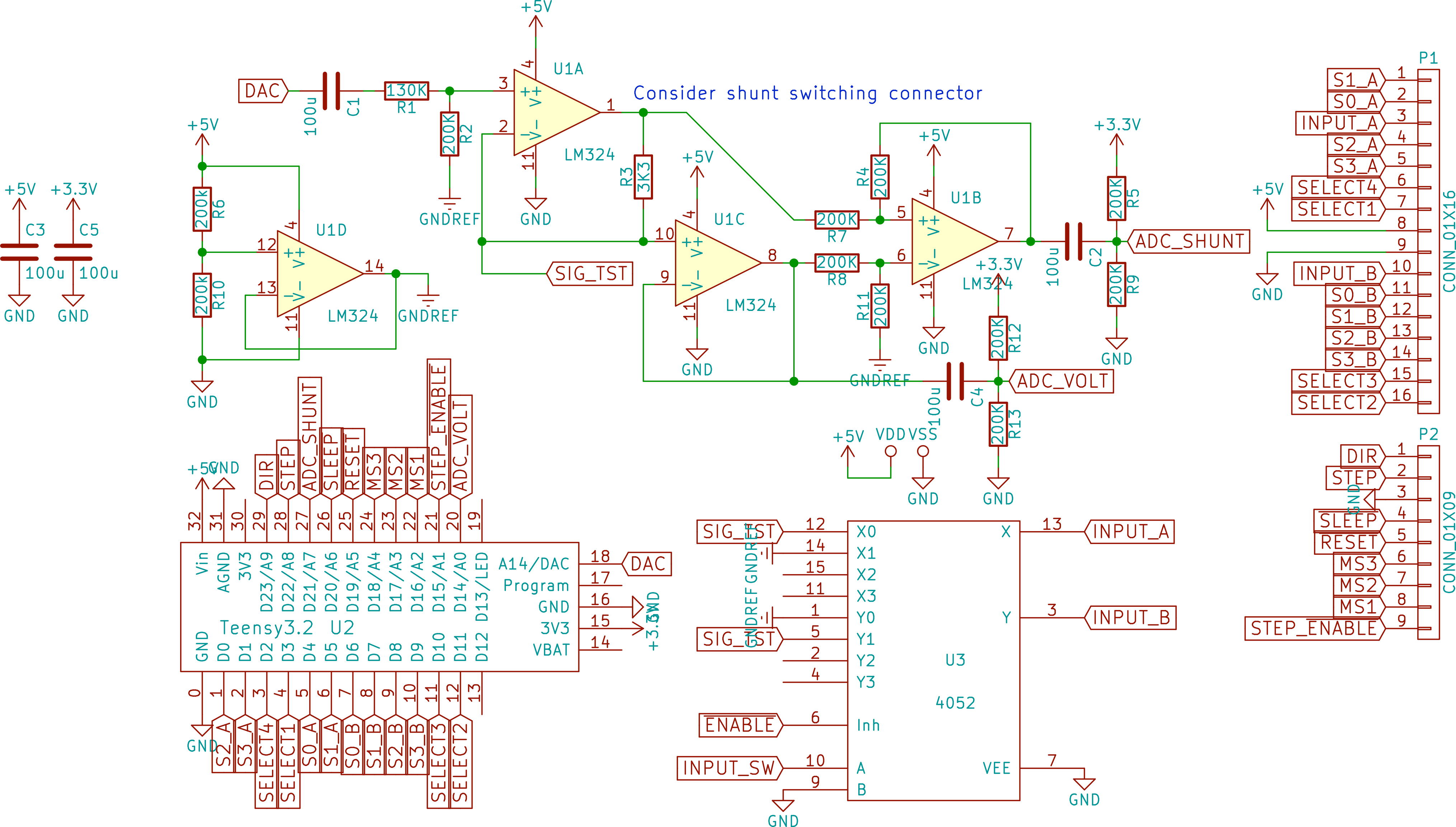
Well, the rest of the signal generator board is just some connectors and decoupling capacitors, so that the whole schematic of the signal board becomes:
![]()
Figure 12: complete schematic of signal generator board.
Well, that's it for the electronics. Hopefully, you learnt something new, and if not, at least you know what makes this design tick.
-
Old problems, new solutions
07/07/2016 at 19:12 • 0 commentsIn the last log, I briefly mentioned what I think were the problems in my old setup to research the influence of flow speed on the electrical behaviour of electrolytic solutions. In this log, I want to go over these problems and discuss the high-level design choices I made to alleviate them.
The longevity of the measurements
While the measurement itself took 2 minutes, the water was pumped between containers, so it had to be pumped back. I also wanted to flush the setup after each experiment, to make sure measurements couldn’t influence each other. All in all, this could make measurements last up to 10 minutes. This may not seem like much, but please consider that I did three different measurements at each flow speed[1], and tested at about 10 different flow speeds.
You can see that collecting all the measurements can take quite a long time. And during this time, temperature can vary, salt can precipitate out of solution, and so on. Because of this, there may be deviations introduced in data, which are undesirable.
Also, the longer the measurements, the less you can perform in a given amount of time. Because of this, I only had one data point for every condition. This means that you can’t average out any inherent deviation in your system, which makes for these unclear correlations. Or in scientific terms: the lower the amount of data points, the lower your significance will be.
We can solve this problem by examining the electrical behaviour of the solution at alternating voltages at various frequencies. This technique is called Electrochemical Impedance Spectroscopy, or EIS. It is much faster, while providing some additional information. I will go into more detail in a separate log.
The function fitting did not work to well
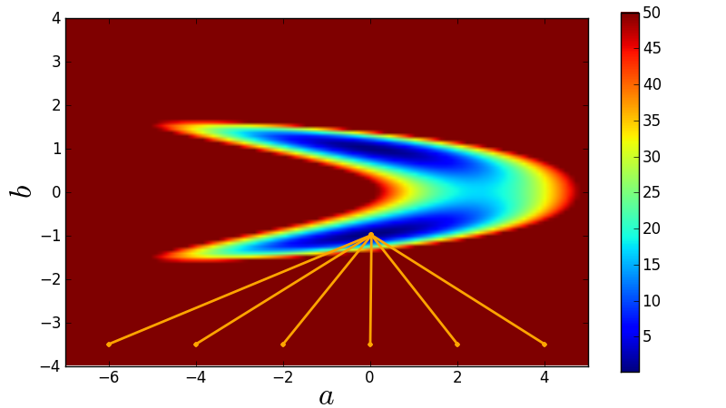
In my previous research, I used what is called a least-squares function fit to fit my experimental data to the theoretical behaviour of the solution.
To understand why this is problematic, we must first examine function fitting in closer detail. A function fitting algorithm is an algorithm that you feed a set of points, your data, and a function that has certain parameters,
would be a basic example. You then give the function fit a guess for what the parameters need to be. It then tries to find the parameters that will make the function go through the data as well as possible.
The least-squares function fitting algorithm is perhaps the most basic widely-used function fit. It basically just tries to minimise the average distance of the data to the function. However, it has the problem that it tends to find local maximums. This picture illustrates this quite well:
![]()
Figure 1: The tendency of a least-squares function fit to find local maximums. From the Python course for MPIA. Copyright 2011, Smithsonian Astrophysical Observatory. Used under a Creative Commons Attribution 3.0 License.
Also, my function had 5 parameters. The more parameters you have, the more difficult it becomes to get a good fit. Needless to say, I had quite a few measurements where the function fit determined that the resistance was very high, while the capacitance was really low, where other measurements where swapped. This made analysis difficult.
I will try to solve this problem by directly calculating the parameters from the data. If I have more data points then needed, I might average the parameters calculated from various samplings of data points together. Whatever I’ll decide, I will probably document it in a log about the software.
The flow speed was not tightly controlled
In my previous research I used a pump to pump the solution through a measurement tube. The pump had no control loop associated with it. Even though it was a pretty strong pump, and hence not influenced by small changes in pressure all that much, it still was a little bit. Because of this, the flow speed wasn’t perfectly constant. Also, due to the mechanics of the pump, it moved the solution with small burst, which also isn’t an ideal constant flow rate. You can see these effects in the graph beneath:
![]()
Figure 1: Weight displaced by the pump over time.
Also, the pump may have sucked up some undissolved salt from the bottom of the solution storage container, so that the conductivity of the electrolytic solution varied, which isn’t ideal.
These effects contribute to the noise in the data, which I want to eliminate. So for this incarnation of my test setup, I am not using a pump to pump the solution along the electrodes, but I am moving the electrodes through the solution. Using a linear slider from Actobotics and a stepper motor, the electrode array can be dragged through a basin with the solution. Since the measurements will be much faster, it is possible to use a rather small basin, in fact I’m using a cake tin. This has the added advantage that the whole solution is easily accessible, so that it can be stirred periodically to make sure there is no undissolved salt.
This works because physics has to be the same, regardless of the reference frame. The only thing that matters for us is relative speed, so whether the solution moves along the electrode, or the electrode moves through the solution, as long as the speed at which they move relative to each other is equal, the situations are physically the same.
These were the high-level improvements I’m making that are driving the design. Let’s dive in the electrical details of that design in the next log.
Endnotes
[1] One with the pump of for calibration, one with the stepped pump, and one actual measurement in case you were wondering.
-
Prior research
07/07/2016 at 13:15 • 0 commentsIn this log, I will try to succinctly explain the information I have gathered on flow-dependent electrical behaviours of electrolytic solutions in basic terms. So let’s start by breaking that sentence down.
Electrolytic solutions
As probably everyone reading this knows, our world consists of tiny particles called atoms. These atoms consist of a positively charged nucleus ‘orbited’ by one or more negatively charged electrons. The positive charge of the nucleus and the negative charge of the electrons cancel out, so that the atom as a whole is neutral. Sometimes, an atom can gain or loose an electron, so that it becomes negatively or positively charged respectively. In this case we stop calling it an atom and call it an ion instead[1].
![]()
Figure 1: Schematical representation of electrolytic solution.
Electrolytic solutions are solutions that contain ions[2]. Salts, a class of compounds, consist of ions. Table salt is a salt. So, table salt in water is an electrolytic solution. In fact, tap water also contains trace amounts of various salts, which makes it an electrolytic solution, just a very dilute one.
The cool thing about electrolytic solutions is that they can conduct electricity. They can because the ions can freely move throughout the solution and where charge can be moved, electric current can flow.
A basic question
About a year ago, I wondered whether the fact that an electrical current can influence the movement of the ions meant that a movement of the solution could also influence this movement, and in turn, the electrical current.
![]()
Figure 2: Early revision of test setup.
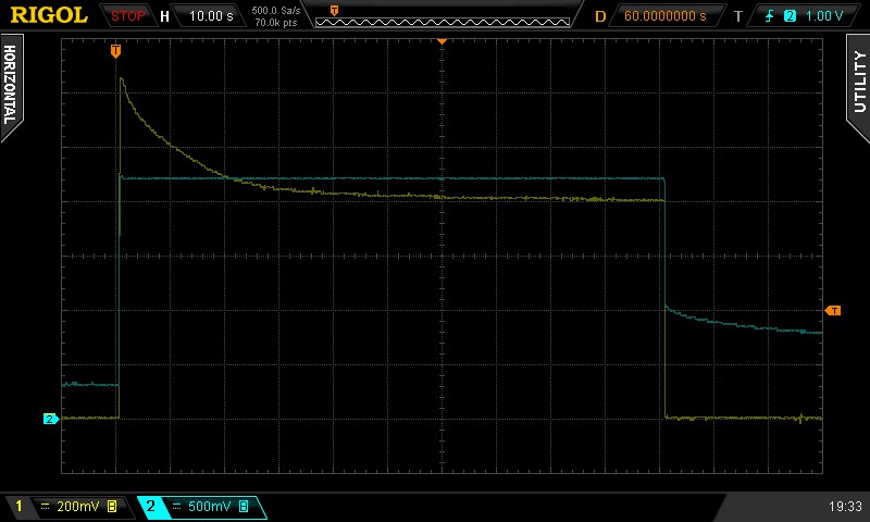
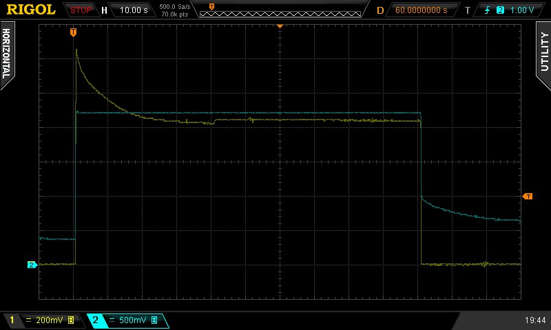
So I did some research. You can read the full thing here, but I will explain the experiment here and now. My setup consisted of a tube, in which 2 electrodes were placed. I actually used OSHpark PCB’s as electrodes, because they are gold-plated, so they won’t erode and are quite cheap for a gold-plated object to get custom-made. I used a pump to pump a solution of table salt in water through the tube for a certain amount of time. During this time, I put a constant voltage over the electrodes and logged the current using a current amplifier and my oscilloscope. I repeated the experiment for various flow speeds.
![]()
Figure 3: Measurement example.
I got results like the above, taken straight from my oscilloscope. In it, the blue trace is the voltage over the solution, while the yellow trace is the current through it, where one mV on the oscilloscope is one uA of current through the solution.
The origin of the results
Where does the curved shape of the current come from? To find the answer, we need to have a closer look at a fairly obscure area of physical chemistry.
As a voltage is applied over an electrolytic solution, the ions start moving towards the electrode that is oppositely charged to them. You would think that this creates a huge separation of ions throughout the solution, but what actually happens is that the ions clump up close to the electrodes, thereby negating their charge, so that the ions in the bulk of the solution aren’t influenced all that much. This cloud of ions close to the electrodes is called an electrical double layer, and its formation is what causes the current to start out relatively high, and taper off towards the end.
You may be wondering now where the base current comes from, since I just mentioned that the ions, which transfer the electrical charge, stop moving after a while.
![]()
Figure 4: Schematical overview of faradaic currents.
This current arises from particles, which are bumped all over the place in a process named diffusion. They react at the electrodes in a redox reaction, thereby gaining or loosing an electron and then diffuse away. Since they basically stole or brought an electron, charge was moved, thus creating an electric current. This current is known as the faradaic current[2].
These two effects shape the equivalent circuit. We model the charging action of the electrical double layers as capacitors, the most basic components for storing charge. The faradaic currents form an additional path for the current to go through, so they can be modelled using resistors in parallel with the capacitors. Then there is also the resistance in the bulk of the solution, due to the drag the ions encounter there. This can be modelled using a resistor in series with our circuit. Keep in mind that there are two electrodes, and that there is a double layer at each of them, so we need two instances of our RC-parallel circuit. Putting all this information together, we get the following circuit:
![]()
Figure 5: Equivalent circuit of electrolytic solution.
Analysis
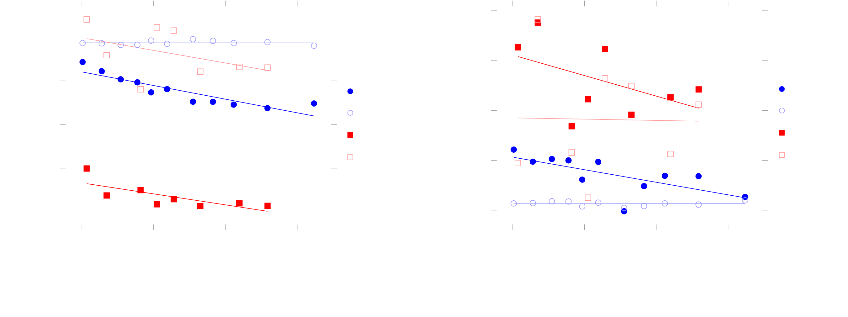
Knowing this circuit, I could find its behaviour by solving a basic differential equitation, again: you can find the nitty-gritty calculations in the full report. I could then fit my data to this behaviour. From this fit, you can calculate the component values in the equivalent circuit. I could then compare those for various flow speeds[3].
![]()
Figure 6: Jumpy current waveform during flow change
I knew there was some change in the electrical behaviour of the electrolytic solution, because I also conducted measurements in which I turned on the pump halfway through, which resulted in a jump in the waveform. What I didn’t know was if this change varied with the flow through the tube. Luckily the calculations yielded an answer:
![]()
Figure 7: Results
There definitely seems to be some sort of correlation going on. My current thinking is that the flow-dependent behaviours are caused by disturbances in the formation of the electrical double due to the flow, but that is hard to say for sure without some advanced mathematical analysis of double-layer formation and some more data. For now, it’s hard to even tell what kind of correlation there is between flow and the equivalent component values. This is because of some problems with my methodology, on which I want to improve in this project:
- The measurements took quite long.
- The function fitting did not work too well.
- The flow speed was not tightly controlled.
I will examine each of these problems in closer detail, along with the solutions, which formed my current methodology, in a later log. With some luck, I can use the data I gather during this project to find out more about the underlying mechanisms causing the flow-dependent electrical behaviours.
So now you know all about my investigations into this topic so far. If you want to know more, tinker around with the data yourself or just have a look at the code I used in my test setup, I will refer you to the full report. If you have any questions, feel free to ask them in the discussion.
Endnotes
[1] Sidenote: there do also exist ions consisting of more than one atom.
[2] A. D. Mcnaught and A. Wilkinson. IUPAC. Compendium of Chemical Terminology, 2nd ed. (the ”Gold Book”). WileyBlackwell; 2nd Revised edition edition. isbn: 978-0865426849.
[3] This is not quite true, but this explanation gives the gist of it. I actually compared the component values to those of a measurement without flow captured close to the measurement and then plotted the deviations in those values versus the flow. This is also why some of the units on the axis don’t match with the story.
Solid state flow sensing using EIS
Investigations into a novel flow sensing technique to create tiny cheap flow sensors, all using electrical impedance spectroscopy.