agp.cooper
-
Programming the Weird CPU
08/04/2016 at 04:11 • 0 commentsProgramming the Weird CPU
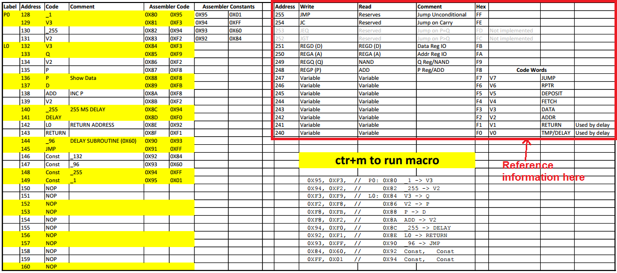
I have uploaded three xlsm files (they contain a macro (ASM) so you need to enable macros to run them).
The three files are:
- Monitor.xlsm
- Program8BitConter.xlsm
- ProgramLEDChase.xlsm
The basic layout is the same:
![]()
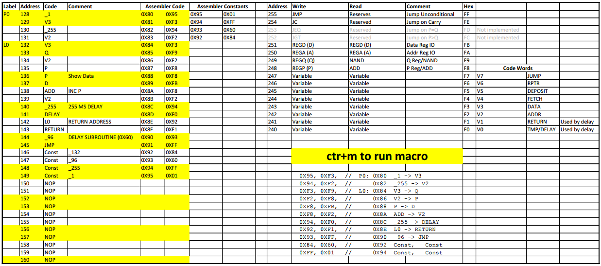
Here is where you enter your code:
![]()
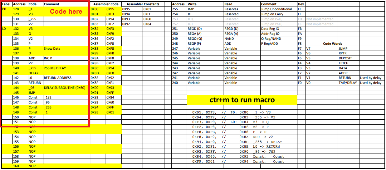
Assembler for the front panel panel here:
![]()
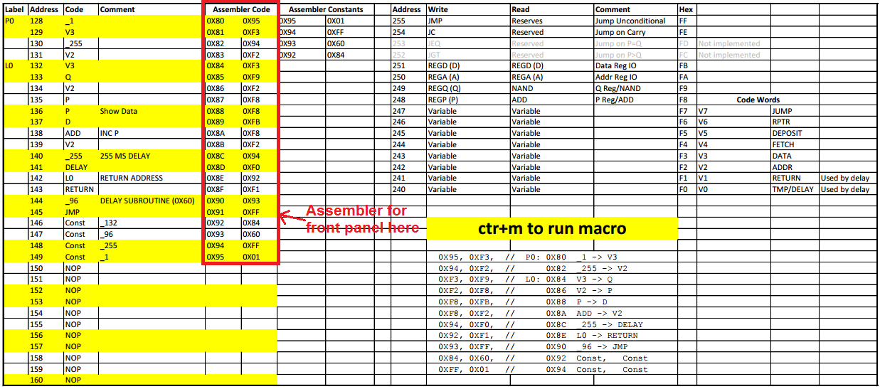
C Code for Arduino here:
![]()
CPU reference information (note aliases used by the macro are listed in the Aliases tab/page):
![]()
And finally a reminder how the run the macro:
![]()
When you run the macro it will ask you for the top of RAM which is where the constants are stored. Answer "149" or more for this program. This is the same program described in the "Details Section" of this Project (if you want to know more about it).
Alan X
-
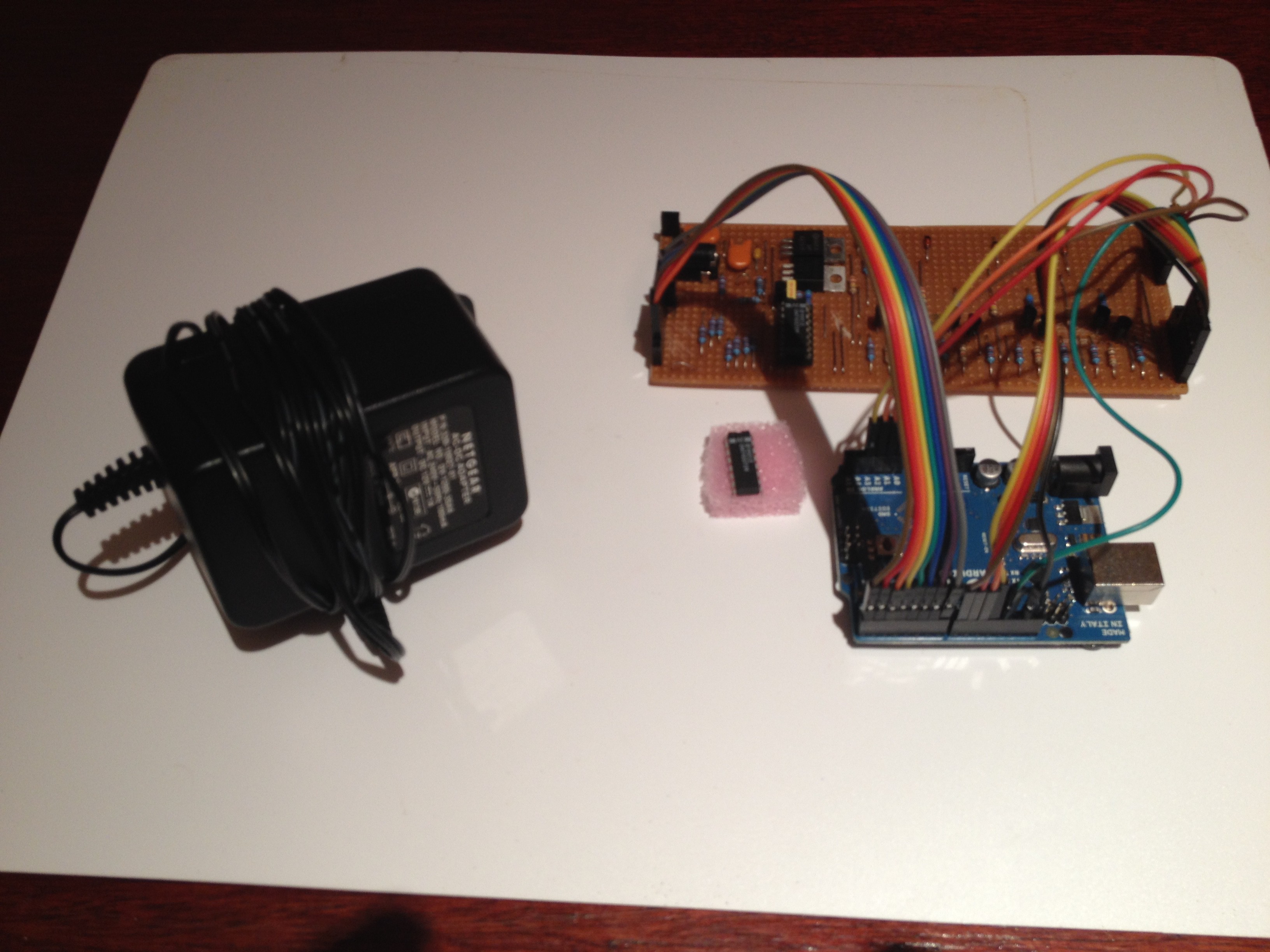
Using the Arduino to debug WCPU
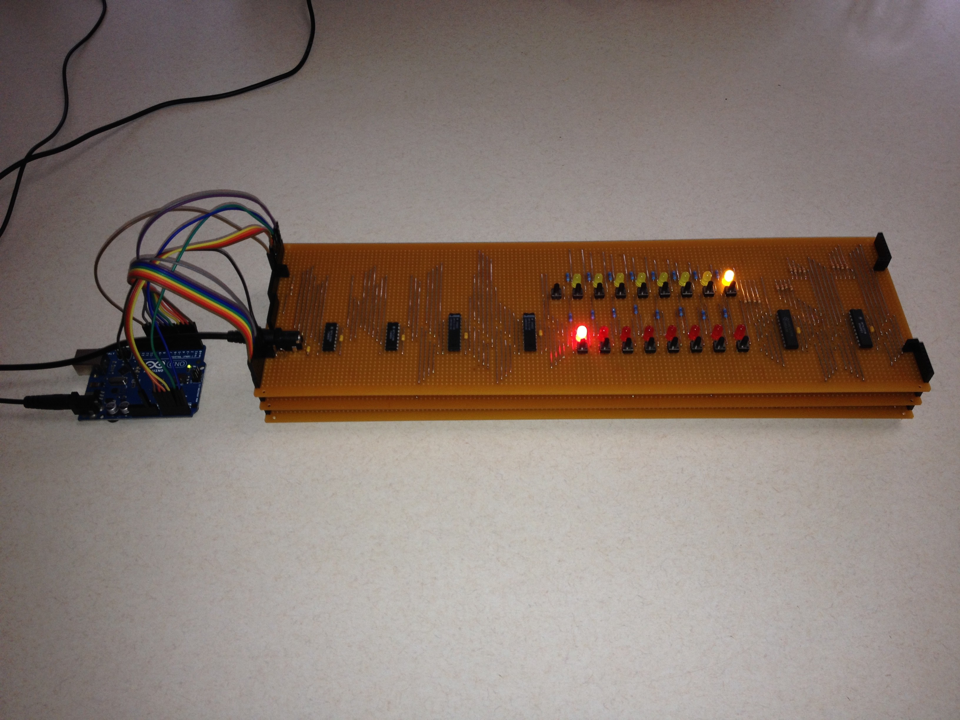
08/03/2016 at 05:33 • 0 commentsUsing the Arduino to test boards
Because of the complex logic I had to use an Arduino to check these everything.
Here is Weird CPU mark I, using the Arduino as a PROM and testing the PC board (the stack consist of the IO board, the timing and memory board (only the RAM is installed) and the PC board). The access time of the Arduino PROM was about 1.3 us so I slowed down the CPU clock from 1 MHz to 100 kHz:
![]()
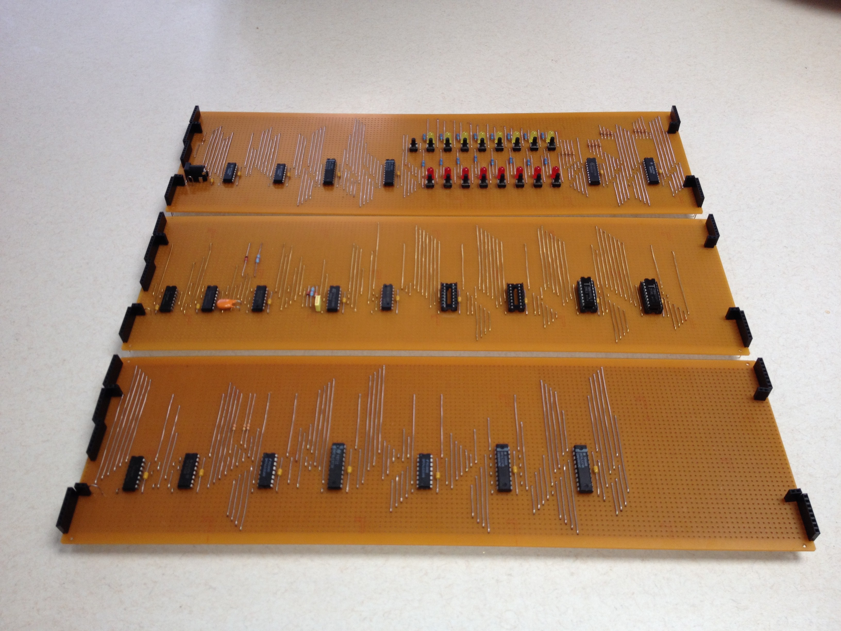
Here is the stack disassembled:
![]()
You may note the repeated use of read and write decoder chips (2) on each board (generally the first two on the left). 41 tracks is not enough to decode all the hardware addresses just once.
Here are the build notes for one of the boards:
![]()
Without the Arduino I doubt that I could have completed the project.
AlanX
-
Reading the schematic of Weird CPU
08/01/2016 at 04:29 • 0 commentsUnderstanding Weird CPU
Now that I have spent some time reviewing other CPU project (it is good that I am not the only mad person out there!), I do find it hard to follow their concepts.
So I will try and breakdown my schematic (divide and conquer!).
Before we begin
One instruction - Move
Basically the instruction is:
Move [PC] -> [PC+1]
The CPU moves the data at the address pointed to by PC to the address pointed to by PC+1. So its a just a fetch and a deposit.
Confused?
Answer the question, how would to move data at one memory location directly to another memory location?
Instructions are memory locations
The memory address for the ALU registers P and register Q are 0xF8 and 0xF9, respectively, but:
- If you read register P (0xF8) you get back "P ADD Q" (not the value you wrote to P).
- If you read register Q (0xF9) you get back "P NAND Q" (not the value you wrote to Q).
By the way, other than SHR (which was an omission) this is a complete set of instructions.
You can software code a P XOR Q in 10 instructions.
Making a jump
To make a jump, write the jump address to the Program Counter (PC) at 0xFF.
The four jump options are:
- 0XFF Jump unconditionally
- 0XFE Jump if carry set for P ADD Q
- 0XFD Jump if P=Q
- 0XFC Jump if P>Q
Accessing the front panel
- The address of the Address IO (the bottom row on the front panel) is 0xFA.
- The address of the Data IO (the top row) on the front panel is 0xFA.
- One trick, the input is inverted (and momentary).
DONE!
The Schematic
The schematic has 28 chips excluding the PROM, RAM,and associated memory address decoder.
Lets kill off the Data IO and Address IO
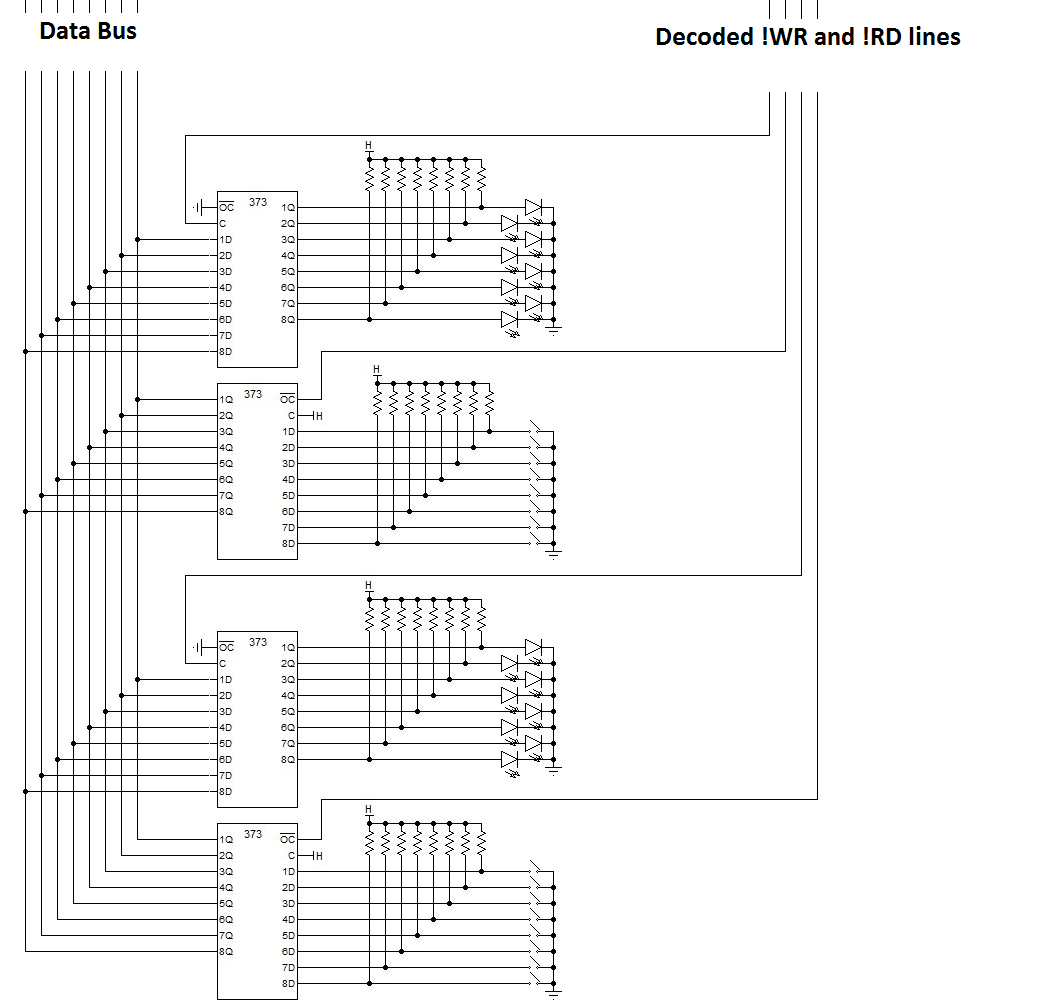
Nothing complicated, just basic input and output (IO) - 24 chips to go:
Note: The "!" in the WR and RD signals indicate active low.![]()
Let kill off the ALU NAND sub-system
Note the ALU sub-systems have common P and Q registers - 21 chips to go:
![]()
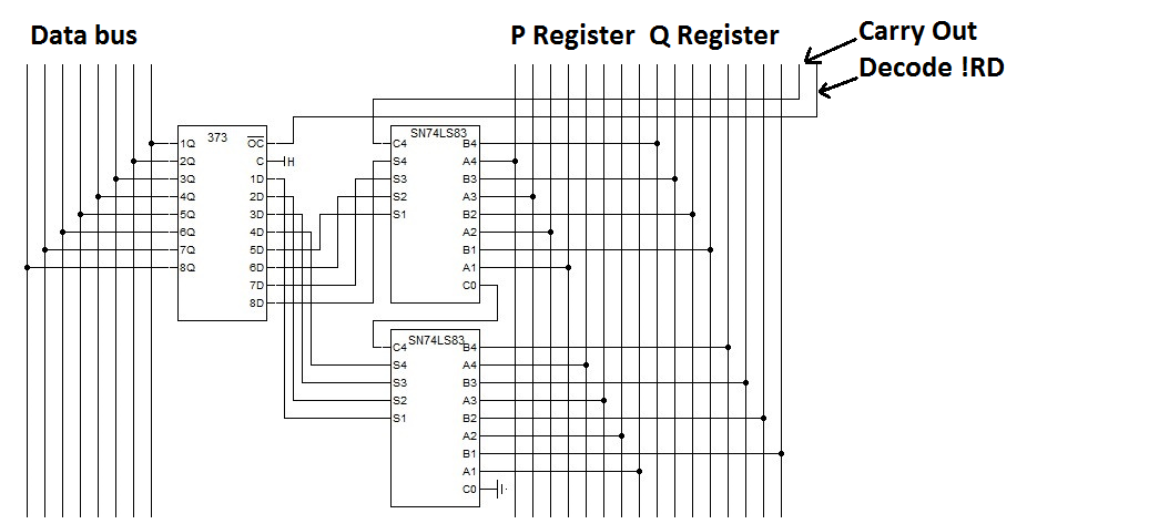
Let kill off the ALU ADD sub-system
Nothing complicated here just two 4 bit adders - 18 chips to go:
![]()
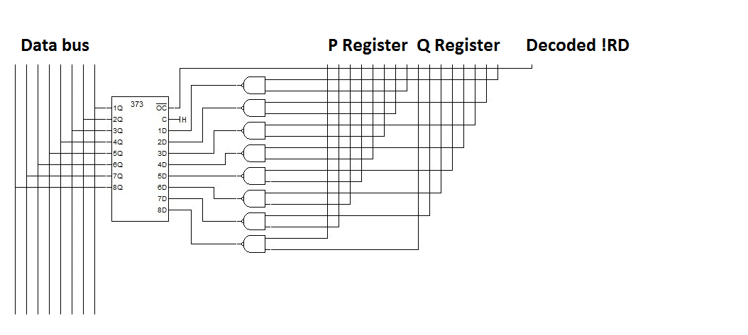
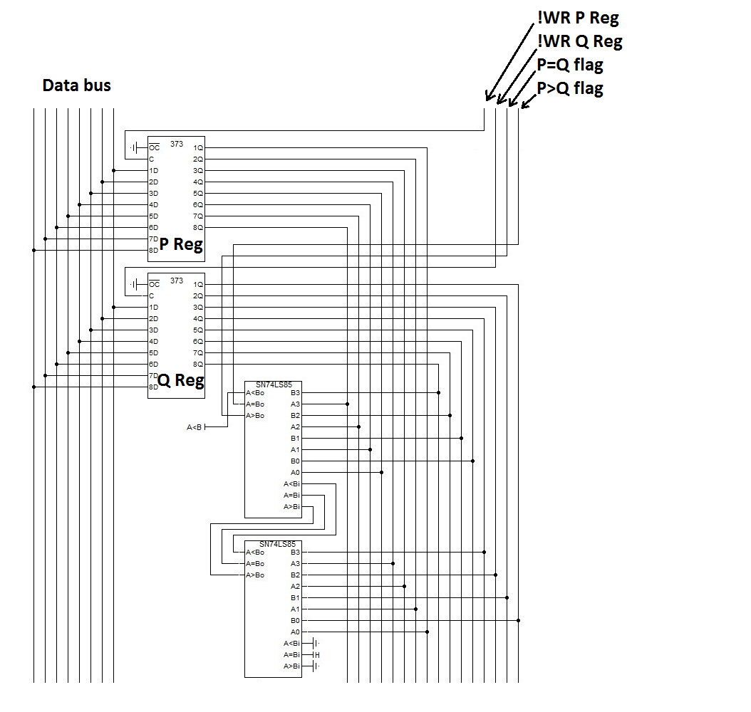
Let kill off the ALU Comparator sub-system
Now we can see the P and Q registers referenced above - 14 chips to go:
![]()
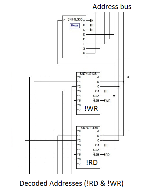
Lets kill off the Address Decoder for the ALU and IO
The decoded address space is 0xF8 to 0xFF but not all are used. Two signal come from the Timing sub-System: !RD and !WR - 11 chips to go:
![]()
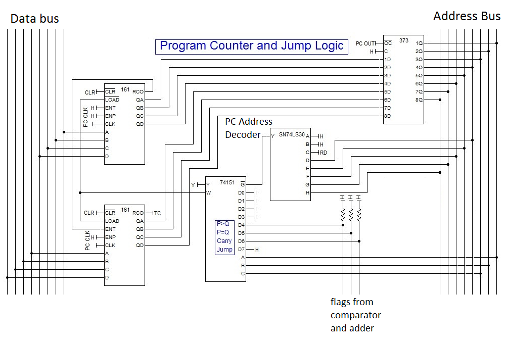
Lets kill off the Program Counter (PC)
This one is a little more complicated as it includes decoding and jump logic. There are a number of inputs from the Timing sub-system (i.e. !CLR, PC_CLK and !PC_OUT) - 6 chips to go:
![]()
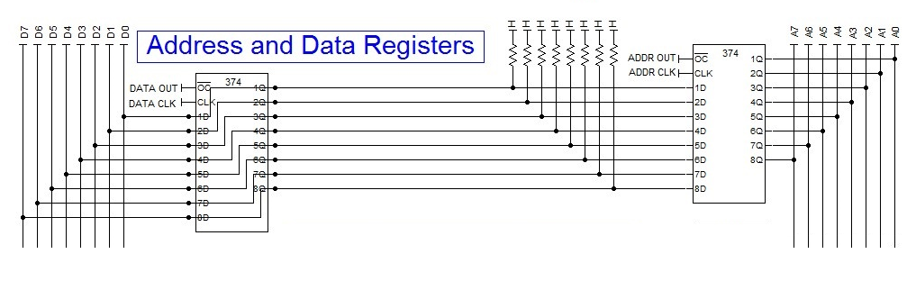
Lets kill off the Fetch and Deposit registers
These two registers (Address and Data) hold the fetch and deposit address (in turn) and the data moved between the fetch and deposit addresses. The PC controls the buses 50% of the time and these registers control the buses the remaining 50% of the time.
The inputs from the Timing System are DATA_CLK, !DATA_OUT, ADDR_CLK and ADDR_OUT - only 4 chips to go:
![]()
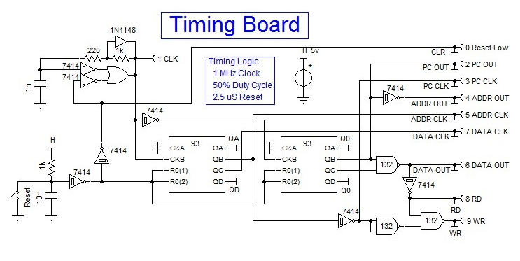
Finally lets kill off the Timing sub-system
What you see here is:
- A clock using a 2 input NAND gate (74LS132). Note that it has been presented as two 74LS14 schmitt triggers and an OR gate. This was necessary because the simulator model for 74LS132 is not actually a schmitt trigger?!
- Reset logic using a 74LS14.
- A two phase clock (74LS93).
- Some timing signal decoding logic.
![]()
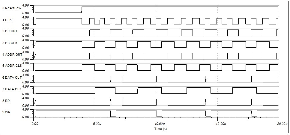
Here is the timing signals from the timing sub-system, it might make more sense now:
![]()
Well, you may not get it all the first time but everything is there for you to understand the Weird CPU.
For my actual build, I did not include the comparator sub-section as Jump On Carry is sufficient for a minimal system.
Weird CPU II has some improvements: 16 bit rather than 8 bit, rearranged instruction addresses and the inclusion of the missing SHR instruction. I have also inverted the jump flags (i.e. Jump on not carry, Jump on P!=Q and Jump on P<=Q).
Your challenge, if you accept it, is to design and build your own minimal CPU with:
- a lower chip count, and
- more instructions.
Best of luck, AlanX
-
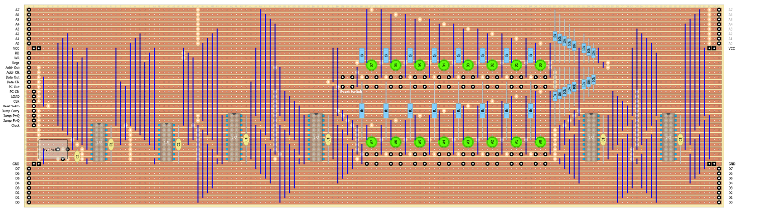
Print to Scale Board Designs
07/31/2016 at 00:46 • 0 commentsPrint to Scale Board Designs
![]()
Added the print to scale (top view) board designs to the file list.
Reverse these (in mspaint) for the reverse side view.
These are the images I used to construct the WCPU.
I kept them up to date as I found errors.
The only board not used in the CPU was the Comparator Board.
While it would be useful it is not necessary.
Jump on Carry is all you really need.
Print to scale is important for reducing errors when cutting tracks and soldering components.
If you do decide to build WCPU then double check everything before cutting a track and work from one side of the board to the other.
A ruler to check cut positions is useful.
AlanX
-
On DIY
07/30/2016 at 03:32 • 0 commentsOn DIY
Having successfully designed and built a reasonable complex project (a TTL computer) I would like to make some suggestions to those who are considering doing the same.
If your a genius then you make your own rules and don't need to consider my learnings.
The key message is that you need structure. It is great fun firing up the soldering iron and doing something but the novelty wears off pretty quickly and the project is soon abandoned. You need a plan before you begin.
So what is structure or a plan?
My structure is based on divide and conquer. Break the project down to smaller sub-projects. How small? That depends on you ability to complete the sub-project.
An example: A discrete transistor CPU
- Design your project (CPU) using standard MSI logic gates (don't worry too much about memory as it is not part of the CPU).
- Redesign the CPU with SSI logic gates.
- Replace the SSI logic gates with discrete transistor equivalents.
Notes:
- MSI = Medium Scale Integration (for example an 8 bit latch or an ALU)
- SSI = Small Scale Integration (for example a quad NAND gate or a Dual D-Flipflop)
- Each stage is complete after you have built and debugged it!
- There are plenty of MSI standard logic gate CPU designs on this forum to get you started.
- Pick one and make it your own (Szoftveres' TTL CPU is worth a look).
- You can easy get someone to review your schematics.
Now even these steps are too big for most people but you get the idea.
Is there a doable path to follow?
You don't need to full populate the plan providing you are confident it is doable when you get there. For example, how to program the ROM can wait.
Testing and debugging
- Me: "Well I have designed and built my CPU but it does not work!"
- My dog: "No surprise, it is to be expected!"
- Me: "?"
- My dog: "Why did you assemble the CPU without testing each component/board first?"
- Me: "!"
A big hint - It takes longer to test and debug a CPU project than to design and built it!
So two things to note:
- Time spent making sure the design is correct is time saved.
- The sooner you test and debug your work the better.
Arduino to the rescue
How did I test and debug my CPU?
I emulated the CPU and CPU components with an Arduino.
Okay, which board would you build first? Did you say the IO Board?
Why, because it is pretty easy to write code for the Arduino to:
- test the IO Board (early visual success)
- emulate the CPU (to test boards and software)
- test the monitor program (with the actual IO Board).
Did I tell you that the monitor program when uploaded to the CPU PROM worked first time! But it did take two attempts to get the Arduino code for the PROM programmer to work (but I had made provision for this).
I wrote quite a few Arduino programs to help me debug my boards.
If you cannot program an Arduino the perhaps you should not be reading this post!
Regards AlanX
-
Added the PROM Programmer the the file list
07/29/2016 at 13:48 • 0 commentsPROM Programmer
One of the sub-projects was to program the PROMs with the Monitor Code. Now I know some guys use a few switches, a power supply and a couple of fly wires! Well some of the schematics were not that much better. But today we have the Arduino so really it is pretty easy. A switchable power supply and some code.
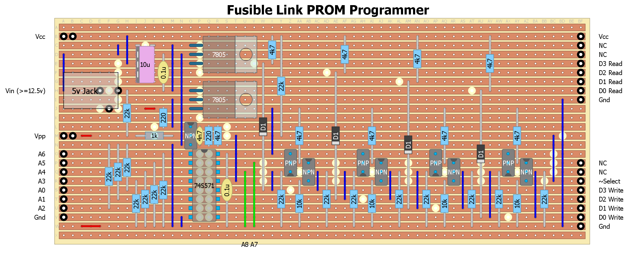
Here is my PROM Programmer:
![]()
The only hard bit is making sure you wire it up correctly. Note the wire colours, same a the resistor codes, so wire 1 is brow, wire 2 is red etc.
Here is the board design:
![]()
You will see two 7805 voltage regulators. One is just a 5v supply and the other switches between 5v and 12.5v (the voltage pulse generator).
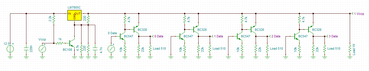
Here is the schematic for the voltage pulse generator (note the load resistors are the PROM loads for the simulation):
![]()
The PROM specifications are quite onerous with regard to voltage slew rate and load impedance thus the fairly complicated circuit.
I also note from the board design that I added data read circuity (the 1n4148 diode and 4k7 resistor).
I have also added the Arduino code for writing the high and low nimbles for the PROM Programmer to my file download list.
AlanX