 [skaarj]
-
Industrial grade PCBs - finally
07/26/2024 at 21:06 • 1 commentAfter some long and busy years:
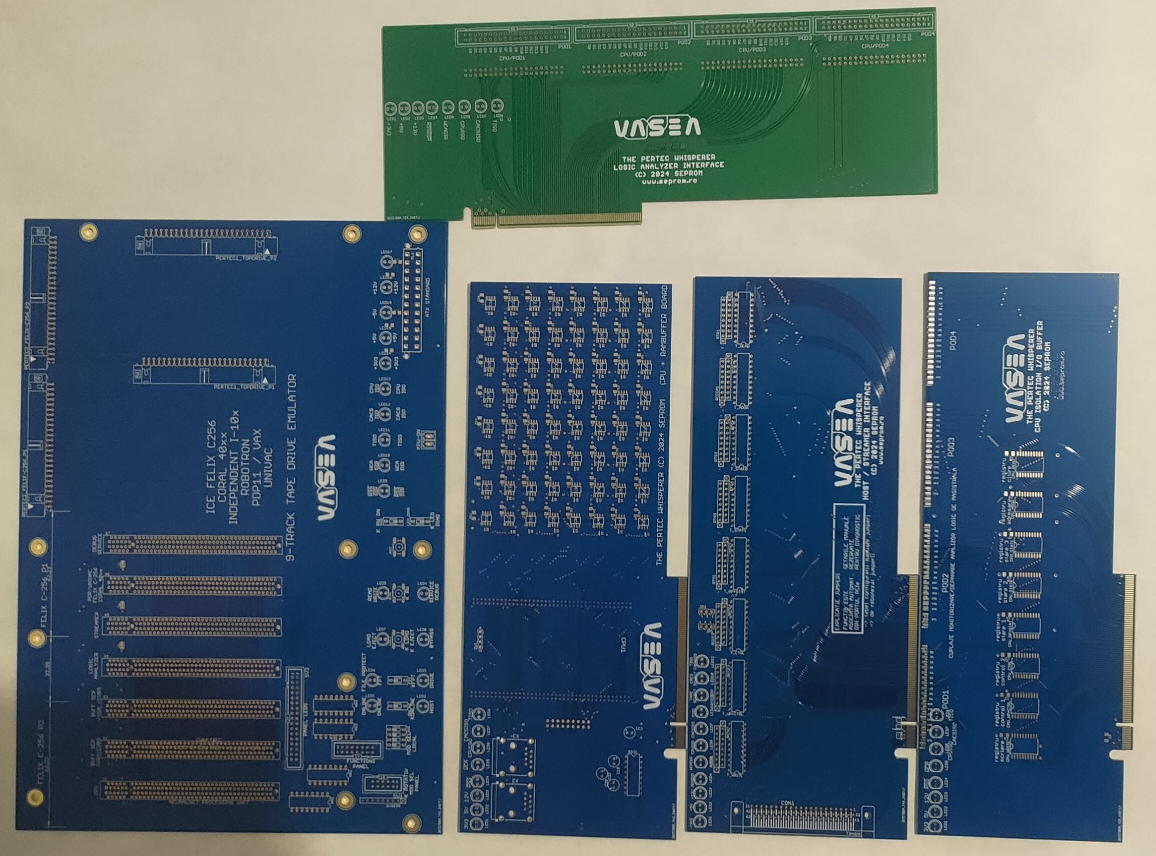
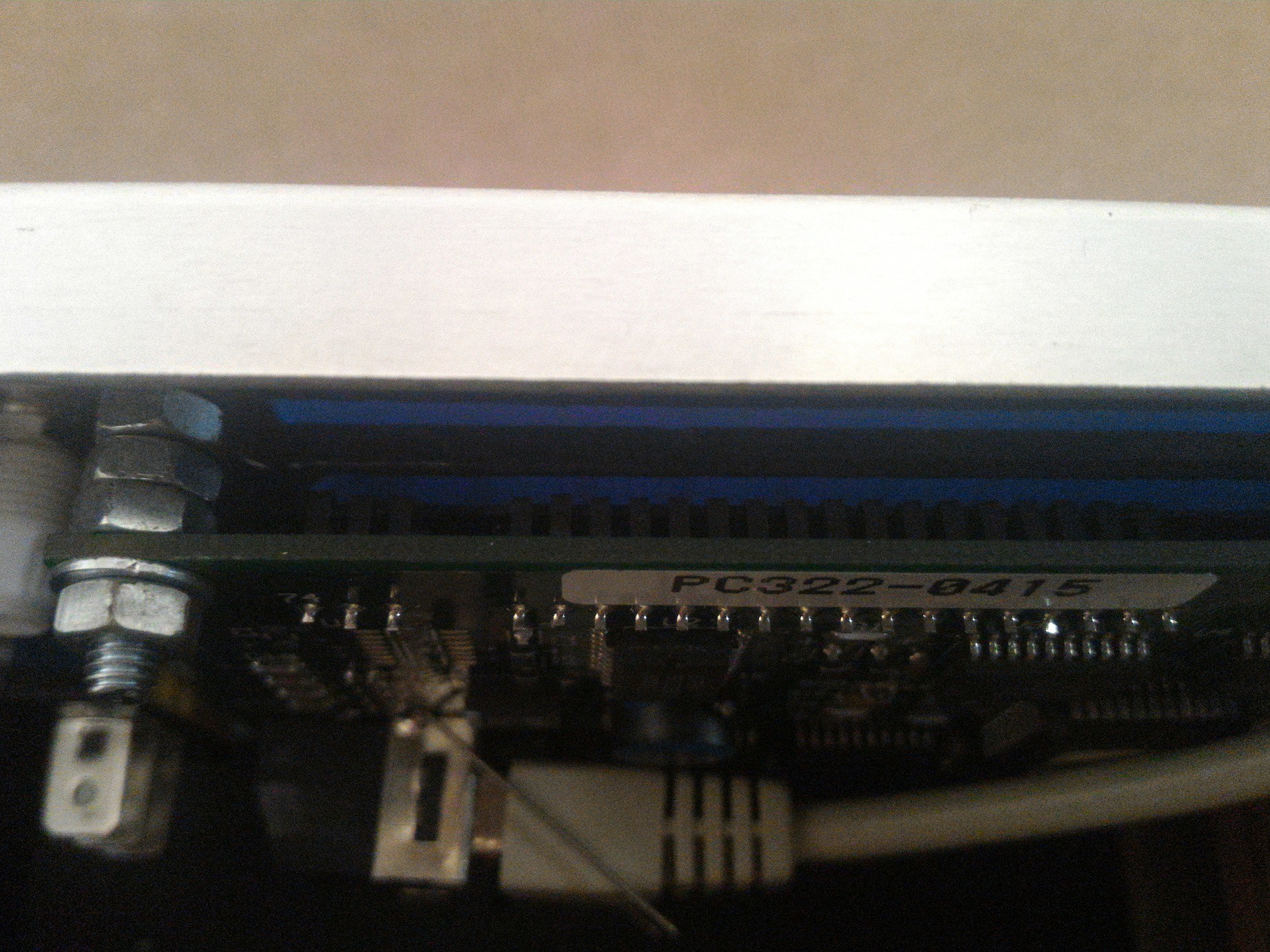
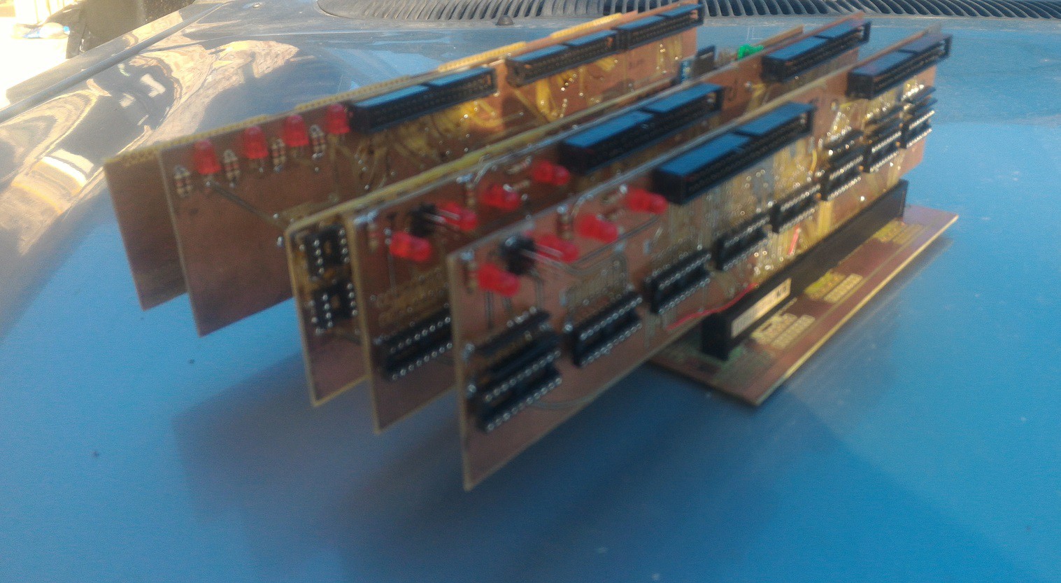
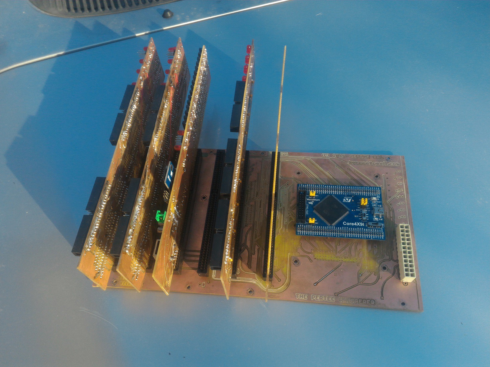
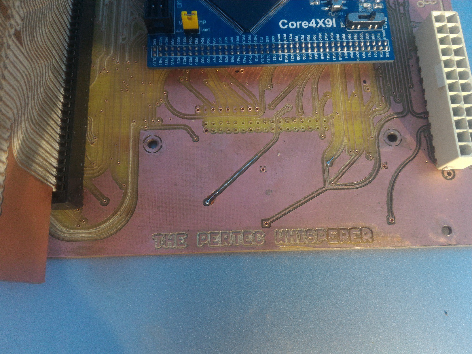
1. Boards set:
- mainboard PCIe backplane with custom wirings;
- logic analyzer interface 1 (green board);
- CPU + ram buffer + sdcard + serial i/o board (right side of the mainboard);
- Host/drive i/o interface for mainframe/tape drive;
- CPU i/o/isolation buffer - right side.
![]()
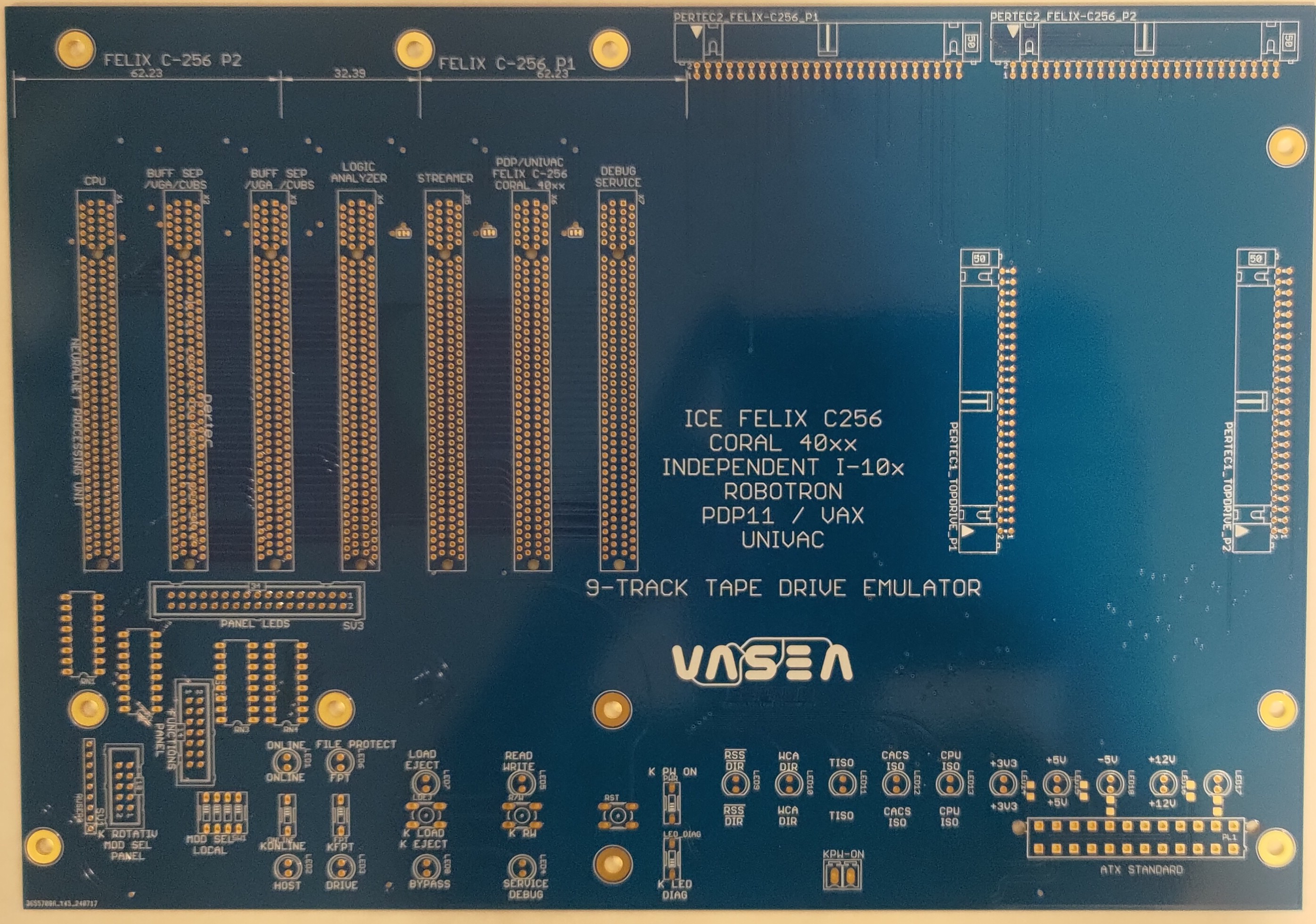
2. Main board
![]()
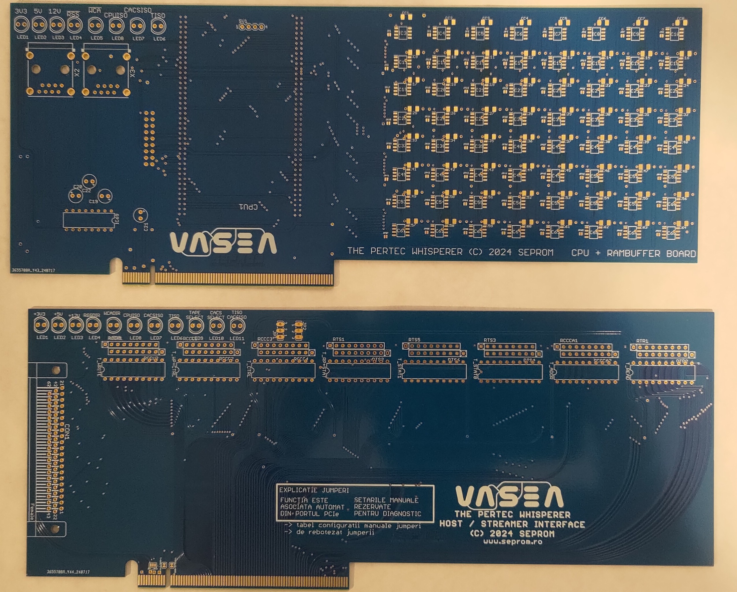
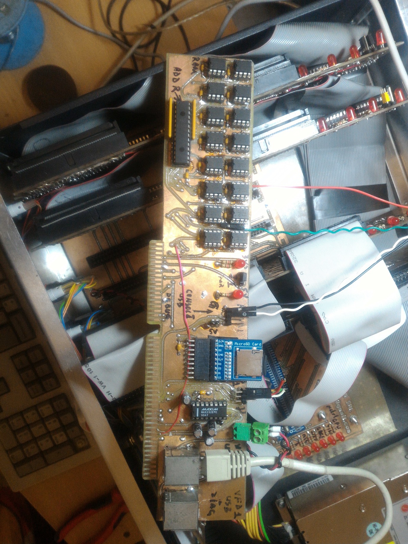
3. CPU + ram buffer + serial i/o + sdcard i/o (top)
Tape Drive / mainframe interface (bottom). In the square there are some magic incantations written in the language of Dracula (Romanian), it says like this: "jumpers explained: function is automatically associated from the corresponding PCIe port. Manual settings are reserved for diagnosis only. To be drawn: -> table with manually-configuration jumpers; -> all jumpers to be re-named (actually "re-baptized" with a new name)
![]()
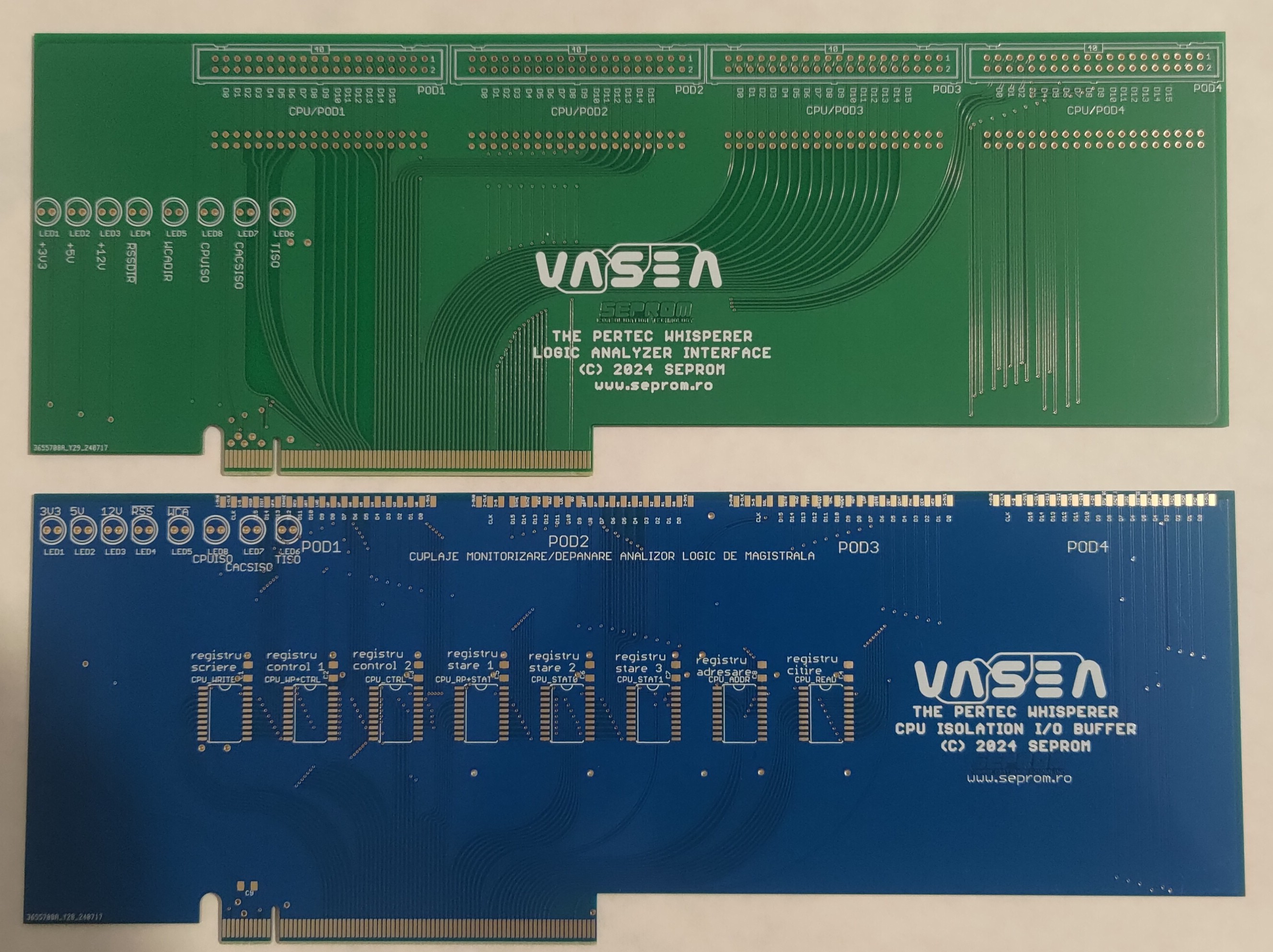
4. Logic Analyzer interface (top, green)
Isolation buffer (bottom).
![]()
Back into the surgery room.
Keep in touch.
[end of transmission]
-
Project video
06/22/2019 at 10:55 • 0 commentsIT WORKS!!!!!!!
-
Whispering in host mode
06/14/2019 at 15:37 • 0 commentsThis one was a little tricky to develop so it took some more time than expected.
Here is what had to be done:
1. Establish communication with the tape drive. For this to happen, the following steps are required:
- select the tape drive using /ITAD lines (transport address 0 and 1);
- issue a short /IFAD pulse of a few uSecs in order to abort any current interruptible operation the tape drive is performing;
- issue a short /IREW pulse to make sure the drive stays at BOT;
- select the data density - 1600 bytes per inch for now: /IWFM+/IEDIT+/IERASE down at the same time, pulse /IGO and those three up.
The tape drive should now issue the following status lines active:
/IONL (online) /IRDY (ready) /ILDP (BOT, begin of tape or load point), /IFPT (file protect) if manually selected on the drive.
2. Start the data transfer:
The data transfer starts when the drive receives a /IGO pulse and the rest is described in the previous chapter - catch /IRSTR, /IDBY, /IFBY and /IFMK using prioritized interrupt lines, fill a 32kB buffer (max buffer size as specified in most of the MsDos pertec drivers), dump it into the SPI RAM Buffer via DMA channel. Each time the entire 2 MBytes RAM Buffer is filled, the operations are paused, the drive waits for a new /IGO while rewinding at the end of the last read block, in the mean time the entire 2 MBytes RAM Buffer is dumped on the microSD card, cleared and the transfer resumes until 2 x /IFMK or /EOT (end of tape) are signaled.
3. Store the data either for fun/inspection/museum purpose or for usage in a physical mainframe environment:
So I have this big chunk of a 40MB 9-track tape drive data dumped inside a microSD card describing some eastern block communist old plans for building the most reliable agricultural tractor in the world. I can either stare at the data - nobody has it in the original format anymore - or I can move things further and load it into a mainframe in order to get access to the top secret development plans.
For the first variant there is no need to replicate the separation into distinct blocks and filemarks.
However if I really want to build my own tractor and take over the fields in my area, I have to push the things a little further and acquire the blocks and filemarks displacement scheme into a map and replicate them by pulsing the corresponding PERTEC lines on the interface while playing in the DRIVE championship.
For various reasons the fatfs library is not capable to handle two distinct files - to store the "map" contents separately. Also the uSD transfer does not work in 4-bit wide bus mode (STM32CubeMX bug) to be able to get things done quickly enough while talking to the drive - good thing I chose to work with a Ram Buffer.
And I am not going to sacrifice an 128k RAM bank just for generating a separate map file and get tons of headaches for not being able to store it separately on the SD card.
4. Welcome to Wonderland: SIMH Emulator has its own format for handling tape images - thank you Chuck for the tip with SIMH .TAP Format which says each block is preceded and followed by descriptors telling details about the current and previous block.
The implemented format looks like this:
---------|--------|---------------|--------|---------------|--------|---------------|--------|---------------|--------|
         |        |               |        |               |        |               |        |               |        |
DATA/BOT | BLKINF |     DATA      | BLKINF |     DATA      | BLKINF |     DATA      | BLKINF |     DATA      | BLKINF |
         |64 bits |               |64 bits |               |64 bits |               |64 bits |               |64 bits |
---------|--------|---------------|--------|---------------|--------|---------------|--------|---------------|--------|
BLKINF (again shorted from Vampires and Warriors tongue ) - block with information. It is inserted before and after each data block.
The format looks like this:
|-------------|------------|
|             |            |
| info prev   |  info next |
|     block   |   block    |
|   32 bits   |   32 bits  |
|-------------|------------|
Each 64-bit block is split into two parts describing what came before and what will come to pass:
- Is there any END OF FILE? (FMK = 1, bit 31)
- Is there any error inside the block which was caused by the tape cloning process? (ERR = 1, bit 30)
- Is this the final data block on the tape? (EOD = 1, bit 29)
- zero bits reserved for future need (bits 28..24)
- How many bytes are there to be read? (BLK LEN, bits 23->0)
I also need information inside "previous record" describing what was before - because tape sequential i/o operations sometimes happen in reverse mode.
          FMK    ERR   EOD    ZERO     BLK_LEN
           31     30    29    28->24    23->0
FMKMASK    0       1    1     1 -> 1     1->1 FMKMASK = 0x7FFFFFFF
ERRMASK    1       0    1     1 -> 1     1->1 ERRMASK = 0xBFFFFFFF
EODMASK    1       1    0     1 -> 1     1->1 EODMASK = 0xDFFFFFFF
BLKMASK    1       1    1     1 -> 1     0->0 BLKMASK = 0xFF000000
Some consideration should be taken regarding the transition between the RAM banks to keep the data integrity and not to lose any data during record transfer. There is no hardware addressing control so everything is at the software level. Special care must be taken at i/o operation for both data and descriptors.
The serial output debug log explains how these first descriptors are loaded from the SPI RAM Buffer into the STM32 memory space:
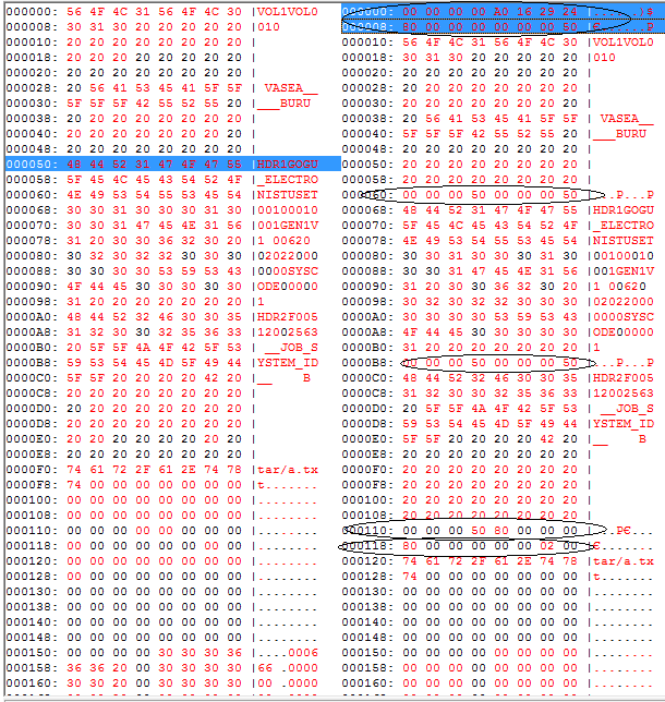
drive_rewind()@tape.c line3701: extract INIT PREVREC:
rambuf_rec_extract()@spiram.c line2851: extract RECORD

ram_extract(spiram.c@line2642): startaddr@0 cbank=0 cpos=0 length=4 free=131071, RAMPOS= 0, RAM_FULL = 0

ram_extract(read@spiram.c line2664): length(4) < free(131071) reading from memory bank 0x0, startaddr=0 cpos=0 length=4 free=131071, RAMPOS= 4
 0x0  0x0  0x0  0x0

rambuf_rec_extract()@spiram.c line2886: FMK=0x0; ERR=0x0; EOD=0x0; BLK=0x0; RECORD=0x0

drive_rewind()@tape.c line3704: init PREVREC:  fmk = 0, err = 0, eod = 0, blklen = 0
#####################################

drive_rewind()@tape.c line3710: extract INIT CUR_REC:
rambuf_rec_extract()@spiram.c line2851: extract RECORD

ram_extract(spiram.c@line2642): startaddr@4 cbank=0 cpos=4 length=4 free=131067, RAMPOS= 4, RAM_FULL = 0
▒)$▒

ram_extract(read@spiram.c line2664): length(4) < free(131067) reading from memory bank 0x0, startaddr=4 cpos=4 length=4 free=131067, RAMPOS= 8
 0xA0  0x16  0x29  0x24

rambuf_rec_extract()@spiram.c line2886: FMK=0x1; ERR=0x0; EOD=0x1; BLK=0x162924; RECORD=0xA0162924

drive_rewind()@tape.c line3713: init CURREC:  fmk = 1, err = 0, eod = 1, blklen = 0x162924, total_tape_length = 1,452,324 BYTES
##############################

drive_rewind()@tape.c line3718: extract 1st PREVREC:
rambuf_rec_extract()@spiram.c line2851: extract RECORD
ram_extract(spiram.c@line2642): startaddr@8 cbank=0 cpos=8 length=4 free=131063, RAMPOS= 8, RAM_FULL = 0
▒
ram_extract(read@spiram.c line2664): length(4) < free(131063) reading from memory bank 0x0, startaddr=8 cpos=8 length=4 free=131063, RAMPOS= 12
 0x80  0x0  0x0  0x0
rambuf_rec_extract()@spiram.c line2886: FMK=0x1; ERR=0x0; EOD=0x0; BLK=0x0; RECORD=0x80000000
drive_rewind()@tape.c line3724: virtual streamer RDY. @start_mainframe() the system waits for /IGO, reads CURREC, transmits the data block and reads PREVREC.
Here is a screenshot of two images of the same tape. Left side is the data alone, right side is the data and descriptors. We can notice the data is padded with spaces to fill the blocks.
![]()
Now let's see what that log and the first 128 bytes in the screen-shot above mean:
Starting at address 0x00000000 - begin of tape image in modified SIMH format:

                    HEX                     BIN                   Activated bits
Previous record: 00 00 00 00  00000000000000000000000000000000   NONE - initial prev record

Current record:  A0 16 29 24  10100000000101100010100100100100 FMK=1 EOD=1 BLKLEN = 0x162924 meaning 1,452,324 bytes or almost a 3.5", 1.44 MB Diskette

Previous record: 80 00 00 00  10000000000000000000000000000000 There was a FMK with zero-block length

Current record:  00 00 00 50  00000000000000000000000010100000 Here it comes an 80-bytes length block:
VOL1VOL0010 [22 x space] VASEA_____BURU [23 x space]   total = 80 bytes
By looking at the tape data header we now know that in the past someone called "Vasili the Weed" came to the factory computing center from the electronics department and wrote that tape containing some files in an old tape archive format, the data was valid for 1402 days (2022 - 620), version one, generation one of the documents and the operating system tape block length chosen at software level is 512-bytes long block split into two sectors of 256 bytes each. We also notice the tape contains an archive format defined by the POSIX.1-1988 specification called USTAR. Bring me some cold beer and I will tell you more.
[END OF TRANSMISSION]
-
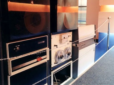
Mainframes behind the Iron Curtain
05/04/2019 at 07:23 • 0 comments![]()
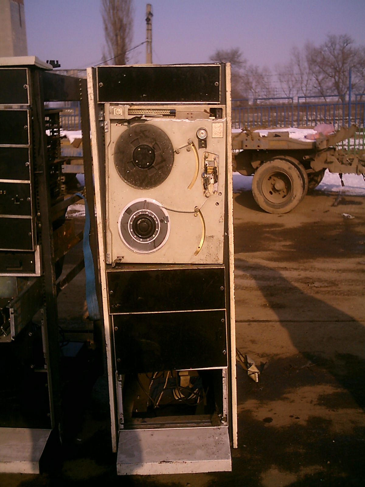
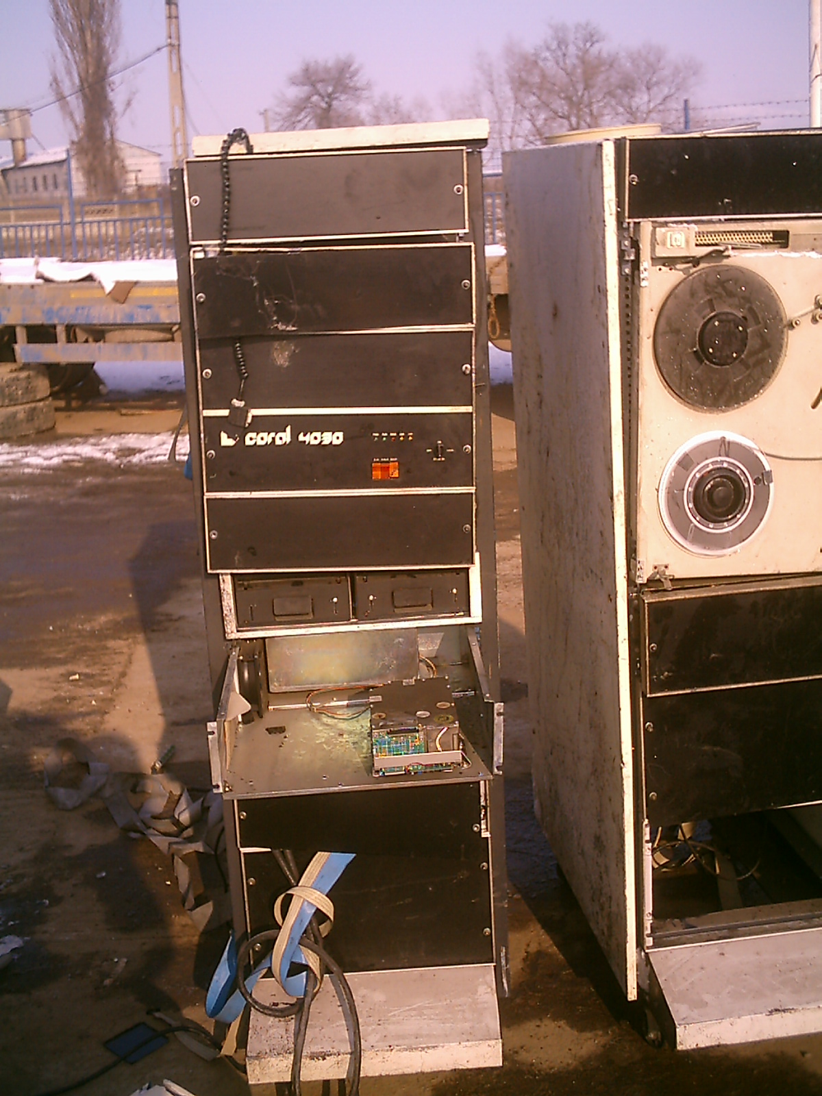
Hackaday covered a very small number of topics about computing technology behind the Iron Curtain, so here is a fresh hot one: [skaarj] is rebuilding a Romanian Mainframe (translated link - this is a very old topic and some pictures or references may be missing). Such pieces of communist technology are pretty rare and most of them require excruciating painful hard work to resuscitate. [skaarj] is not entirely sure which mainframe type to chose from the three dinosaurs roaring in Romania's computing centers during those dark prehistoric times: FELIX, CORAL or INDEPENDENT, as the components are pretty rare, in very bad shape and whatever parts he managed to salvage... come from all three types. Due to their proven performances, those three names were a shock for the COMECON market controlled by the Soviet Union, so Big Uncle Bear officially restricted any exports through special directives straight from Moscow. To avoid the typical anger, some government sources explained the decision to Romania's beloved leader due to CORAL and INDEPENDENT performances being far superior to the USA's PDP.
So far [skaarj] managed to recover three from a Felix-type mainframe, some parts from a CORAL 4030 mainframe, a broken tape drive from an Independent i-100, a Siemens Sinumerik punched paper tape reader from a Felix-M18 and some various peripherals such as 8" floppy drives, huge hard disks, cassette tape drives or various circuit boards. The clumsy serial terminal called DAF-2020 (Display Alpha Numeric) is already up and running, and through the courtesy of [Nico] the future mainframe will be able to access PERTEC-interfaced peripherals through a PERTEC to SCSI converter.
Since the central processing unit (drawer) released its magic smoke in the final agonizing days of the communist regime while running a modified smuggled copy of RSX-11 Operating System, [skaarj] decided to hook a Marvell OpenRD Ultimate Development Platform and install FreeBSD Unix to get access to the functional peripherals and to experiment with ferrite core memory banks. Check the videos on the project main page.
-
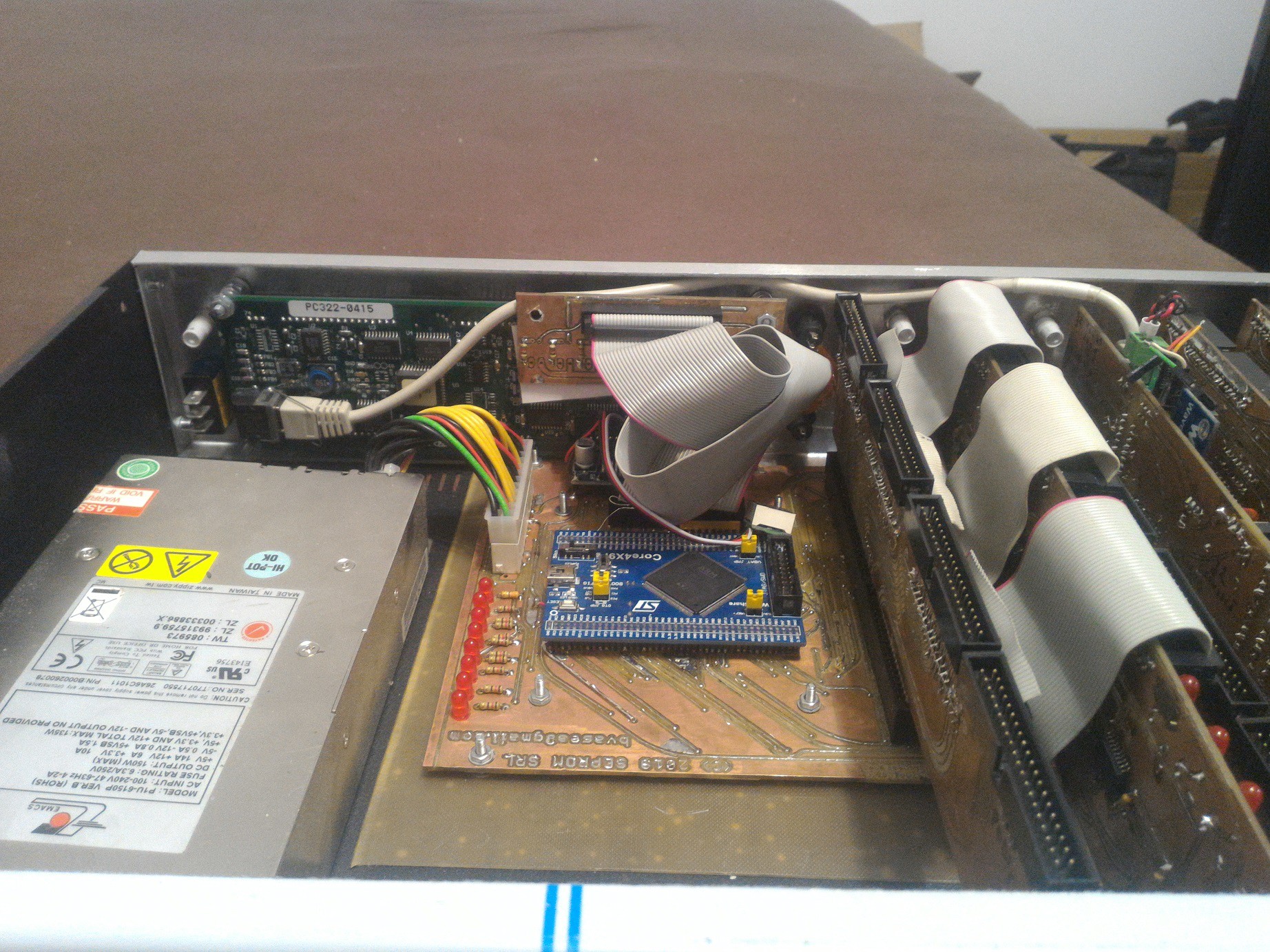
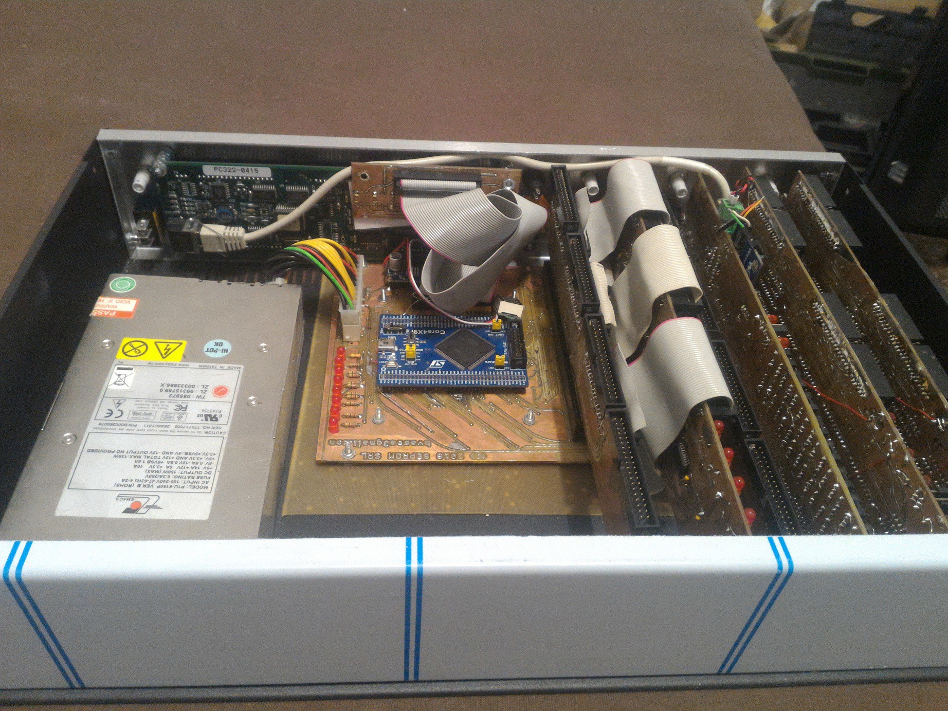
RAM BUFFER
04/19/2019 at 20:28 • 0 commentsData needs to be read fast and precious time is waisted with traditional approach:
- continuous reading of GPIO ports and wait for them to confirm the data is ready for pick-up;
- store the byte inside a variable;
- convert from IBM-style to normal style using either math or a lookup table (faster!), invert the byte
- append the byte to the end of a string;
- push each string to microSD card at every end-of-block;
- try to catch a new read and try not to lose data if all the above tasks together take more than 1.2 microseconds to finish.
All these operations waist precious time so special measures had to be taken:
1. Pertec works in inverted logic (0V means true, 5V means false). This allows for long cables and little noise influence but requires special attention at software level, so each buffer contains the Soviet Union equivalent of 74ALS640 / 74ALS642: the K555AP9. This inverts the received data - thus saving precious CPU time and also making the programming easier without any software inverted logic.
The "normal" circuits were tried first:
- non-inverting data output 74LS/ALS/HC/HCT/N/S-245, 74LS/ALS/HC/HCT/N/S-641,;
- inverting data output 74LS/ALS/HC/HCT/N/S-640 and 642, both normal and -1N variant (double miliamp output signal intensity)
All of them in SMD and THT variants.
Either I bought a lot of trashed parts from respectable, unquestionable great suppliers - which I seriously do not believe - or the soviets had a better design because the 'normal' (74-series) circuits caused surges in the power supply unit in bypass and service mode and they became extremely hot. At first I could not believe and I blamed the soviet chips for destroying my tape drives and my Pertec controllers. I developed a theory about black holes feeding on $$, explained later in this text.
Anyway - I saved a lot of CPU time by passing all byte-inverting operations to external circuitry.
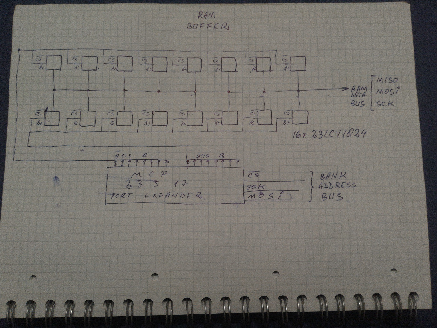
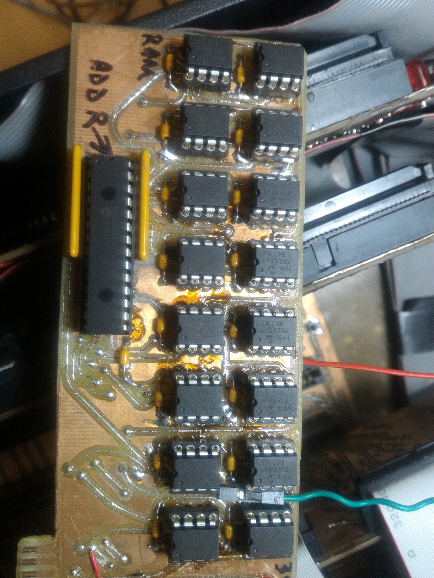
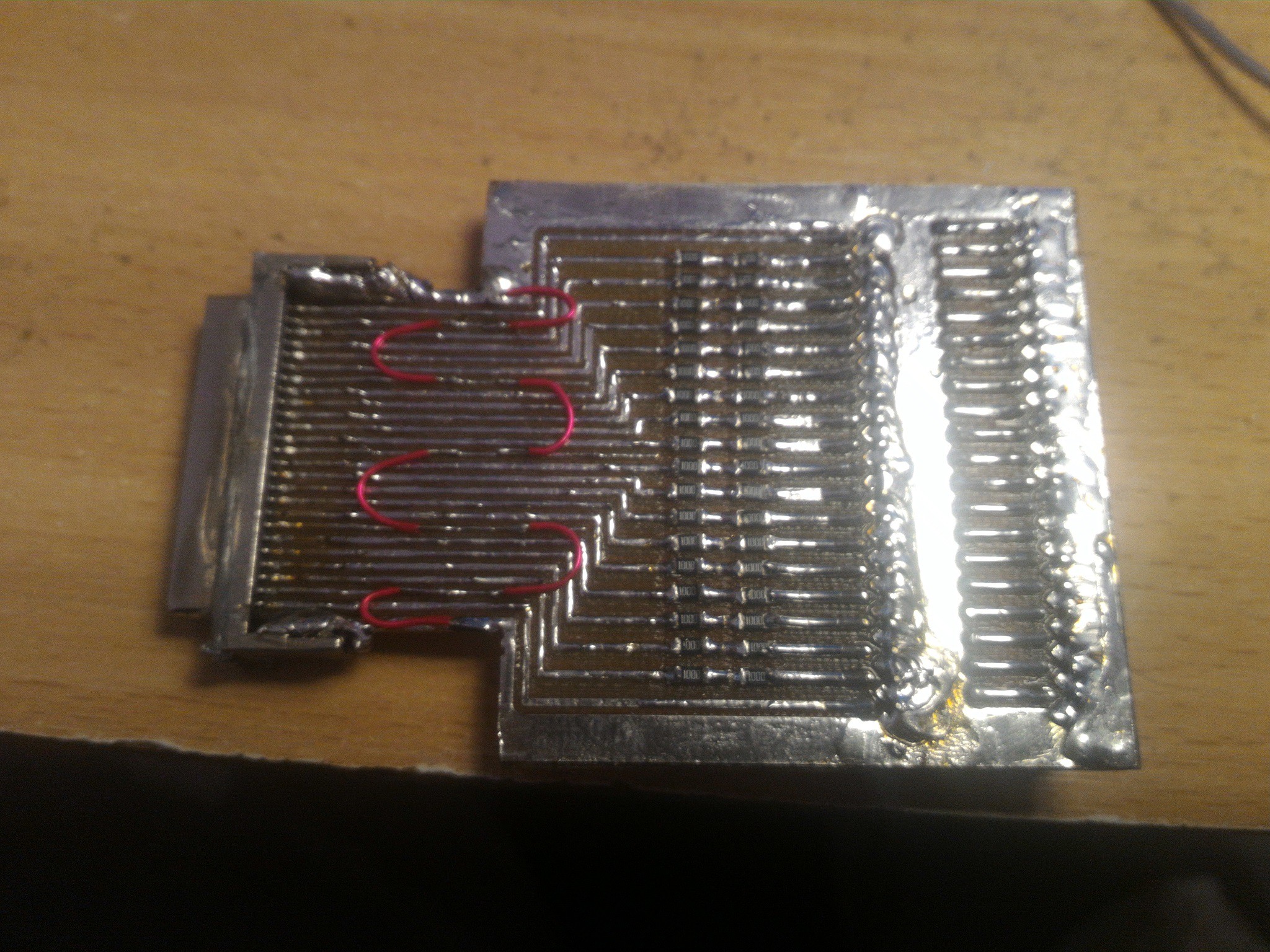
2. Build a fast ram bank using 16 x 23LCV1024 (128 kBytes) high speed serial SRAM.
![]()
As a note: I don't use commercial measurement units. They are lies and blasfemies for the technical part: a Megabit counts stuff to trick people. It is an advertising measurement unit which lies about how great is to see the data rate 8 times bigger, larger and faster than the reality.
![]()
A Megabit is some kind of eye drops Viagra: you drop it in the eyes and see things eight times bigger.
A megaByte represents a quantity useful in computing and it is 1/8 of a megaviag..bit. The French are wise - they say "mega-octet" to avoid tricking people and I respect them for that.
So 23LVC1024 holds 128 kBytes - the great "Megabit" which represents around 9% of a 3.5", 1.44MB floppy disk.
Using 16 of them I built a 2 MBytes RAM bank with custom addressing control.
![]()
This is the system RAM buffer + uSD storage + serial communication.
The addressing is performed via one MCP23S17 SPI Port Expander from Microchip, thus saving 13 i/o pins on the controller side: 16 chip-select + 3 SPI without the PEX, only 6 SPI pins with the PEX. More RAM, more port expanders (PEX). If a lot of RAM, the addressing expanders can be.... selected using another PEX. Or a FPGA logic approach which saves a lot of space, time and speed. It's starting to sound like some $$-absorbing black hole theory.
3. I also defined two DMA stream channels to get the fastest speed available for these 23LCV1024 - actually they should be called 23LCV128kB - circuits according to their datasheet. However the addressing control do not support DMA so this slow things down for a bit. Not megabit.
4. Interrupt requests. A design flaw in the schematics turned to be tricky at software level because in STM32F429 microcontroller, the External Interrupts 9->15 treat all GPIO pins 9...15 from all the ports at the same time and it is not possible to set different priorities for each pin. It may be required to rebuild the motherboard as it is already cut and patched in many places due to the CNC faults.
When performing tape i/o data operations, the ram buffer is used and the corresponding DMA channel is activated for either Tx or Rx data.
__________________________
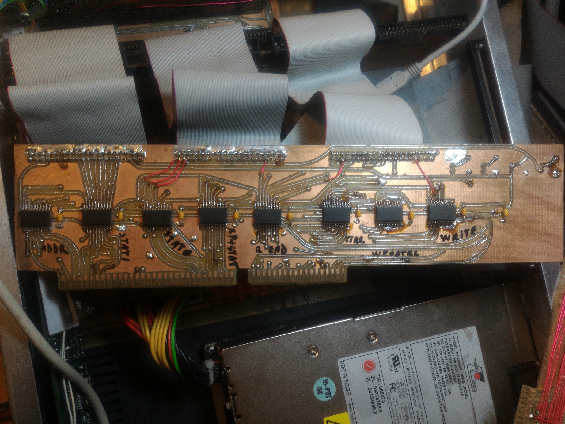
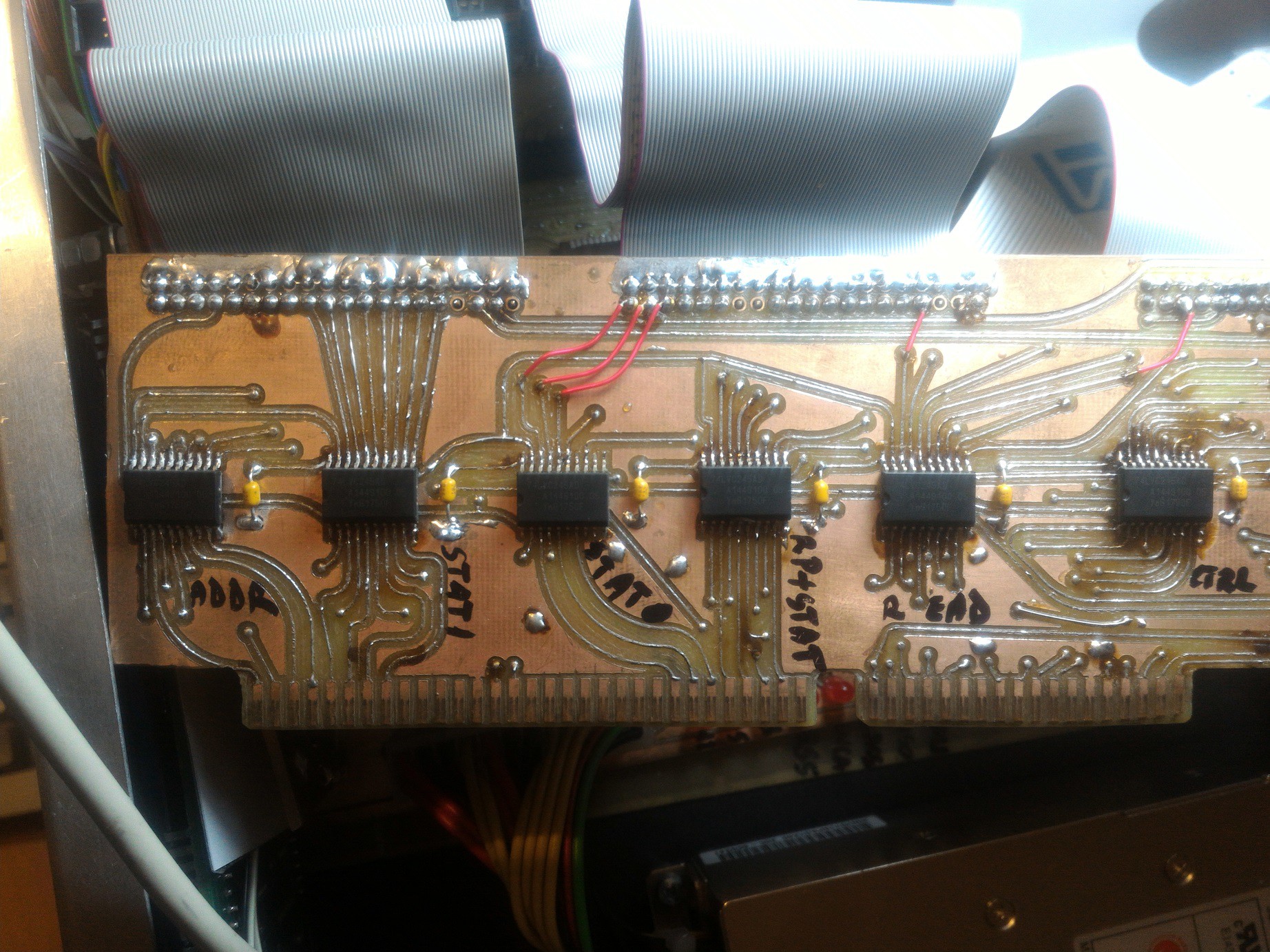
Level shifting, bidirectional i/o data buffer for the STM32F4 microcontroller
![]()
From write to left, first failed experimental buffer built with 74LVC245AD - 5V tollerant, 3.3V powered SMD, now working with 555AP9 (military grade):
Write, Write Parity + Control, Control, Read, Read Parity + Status, Status 0, Status 1, Addressing.
![]()
All the groups are defined in the code section inside the previous log.
[END OF TRANSMISSION]
-
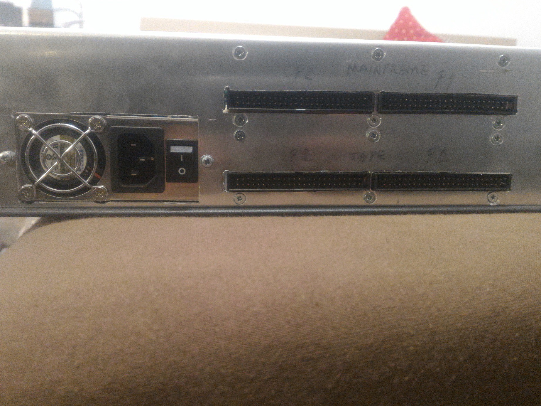
Pertec Interface Signals
04/19/2019 at 19:17 • 0 commentsAccording to the great Archive stored by Bitsavers and after also consulting this amazing Pertec interface explanation at Sydex Inc., the Pertec interface consists of the following:
- Connectors: some times 1 x DB62M - tape drive cable, DB62F controller side, some times 2 x Card Edge (CE)50M - tape drive Pertec formatter or CE50F on the cable each marked P1 and P2, J1 and J2.
Both connectors have almost the same signals. Some drives support all of them, some drives just a part of them.
The following signals correspond to all 1/2" 9-track tape drives with densities of 1600 Bytes per Inch (BPI), 3200BPI and 6250BPI, both Phase Encoding and Group Coded Encoding methods:
/* test write  IW0....IW7
                            [W7] [W6] [W5] [W4] [W3] [W2] [W1] [W0]
                     15  14  13  12  11  10   9   8   7    6    5    4    3    2    1    0
         PB   0   0   0   0   0   0   0   0   0    0    0    0    0    0    0    0
  [WRITE]                                 X    X    X    X    X    X    X    X
 [WRMASK] 1   1   1   1   1   1   1   1   0    0    0    0    0    0    0    0
    WRMASK = 0b1111111100000000 = 0xFF00;
*/

// Write lines - IBM-style ordering, meaning Bit 0 = MSB,
// Bit 7 = LSB

/*   test IWP   PB8
                                    [WP]
         15  14  13  12  11  10   9   8   7   6   5   4   3   2   1   0
     PB   0   0   0   0   0   0   0   0   0   0   0   0   0   0   0   0
 [IWP]                                X
 [WRMASK] 1   1   1   1   1   1   1   0   1   1   1   1   1   1   1   1

WPMASK = 0b1111111011111111 = 0xFEFF;

*/
// IWP  Write parity - odd parity computed over IW0–IW7
// and on some drives is ignored and computed by the formatter.


// CONTROL SIGNALS
// Activated by the controller/mainframe side - operations
// for the drive to execute

/* test CTRL0  PB9...PB15
       HISP EDIT WFM ERASE REV  WRT LWD
         15  14   13  12    11  10   9   8   7   6   5   4   3   2   1   0
     PB   0   0    0   0     0   0   0   0   0   0   0   0   0   0   0   0
  [CTRL0] X   X    X   X     X   X   X
 [C0MASK] 0   0    0   0     0   0   0   1   1   1   1   1   1   1   1   1
    C0MASK = 0b0000000111111111 = 0x1FF
*/

#define ILWD    0x200  //  Last word—Used to tell drive that this is
                       // the last word (byte) to be written
                       //  in this record, Must be asserted at least
                       // 300 nsec. before trailing edge of final
                        //  IWSTR pulse.

#define IWRT 0x400   // Write — When asserted with IGO begins a write sequence.

#define IREV    0x800   // Reverse — When asserted, indicates operation is
                        // to be performed in the reverse direction.

#define IERASE 0x1000 // Erase—When asserted with IWRT and IGO,
                      // causes tape to be erased, usually for a
                      // predetermined length. Usually used to
                      // recover from write errors or provide extra
                      // space for mode changes (Read after write).

#define IWFM 0x2000   //  Write filemark; When asserted with
                      // IWRT, writes a filemark.

#define IEDIT 0x4000  // Edit—Not implmented on all drives.
                      // modifies/updates records inside tape files.

#define IHISP 0x8000  // High speed select—When asserted 1 µsec. before
                      // and then with IGO (de-asserted any time after
                       // the trailing edge of IGO selects high-speed
                        // (streaming) mode.

/*
  test CTRL1
                                               RTH1 RTH2 REW RWU LOL GO
        15  14  13  12  11  10   9   8   7   6   5   4   3   2   1   0
    PC   0   0   0   0   0   0   0   0   0   0   0   0   0   0   0   0
[CTRL1]                                          X   X   X   X   X   X
[C1MASK] 1   1   1   1   1   1   1   1   1   1   0   0   0   0   0   0
[C1MASK = 0b1111111111000000 = 0xFFC0
*/

//CTRL1:

#define IGO   0x01  // Initiate command—Pulsed low for at least 1µsec.
                    // to start command execution. The formatter address
                    // lines must be stable throughout the pulse and
                    // until IFBY drops.

#define ILOL  0x02  // Load on-line—Pulsing this line at least 1µsec.
                    // begins the tape load sequence on many drives.

#define IRWU  0x04 //  Rewind and unload—A pulse of at least 1 µsec.
                    // initiates a rewind-with-unload and sets
                   // drive offline. Some drives require that IREW is
                   // also asserted.

#define IREW  0x08 // Rewind—A pulse of at least 1 µn;sec. starts the
                   // tape rewind sequence. Completion is
            // // signalled by IRWD and IRDY being asserted by the drive.

#define IRTH2 0x10 //  Write density select 2—On some drives, this signal,
                   // along with IRTH1 is used to
                   // select the drive write density. If it is implemented,
                   // it is valid only at BOT and must be asserted with IGO
                    // during the first write sequence.
#define IRTH1 0x20      //


/* test ADDR
                                                         FEN TAD1 TAD0 FAD
          15  14  13  12  11  10   9   8   7   6   5   4   3   2   1   0
     PF    0   0   0   0   0   0   0   0   0   0   0   0   0   0   0   0
[ADDR]                                                     X   X   X   X
[ADDRMASK] 1   1   1   1   1   1   1   1   1   1   1   1   0   0   0   0
 ADDRMASK = 0b1111111111110000 = 0xFFF0
*/

#define IFAD  0x01  // PF0    Formatter address
#define ITAD0 0x02 // PF1 Transport address bit 0 (MSB!)—Used to address
                    // multiple drives on a single controller.
#define ITAD1 0x04 // PF2   Transport address bit 1 (LSB!)
#define IFEN  0x08 // PF3 Formatter enable — This signal should normally
                   // be asserted all the time.
                  //  If dropped for a minimum of 2 µsec., aborts any
                  // comman that asserts IDBY
                  // (I/O, skip, but not rewind or unload).

// #########################################################

/* test READ
                                          [R7] [R6] [R5] [R4] [R3] [R2] [R1] [R0]
          15  14  13  12  11  10   9   8   7    6    5    4    3    2    1    0
     PE    0   0   0   0   0   0   0   0   0    0    0    0    0    0    0    0
   [READ]                                  X    X    X    X    X    X    X    X
[READMASK] 1   1   1   1   1   1   1   1   0    0    0    0    0    0    0    0
 READMASK = 0b1111111100000000 = 0xFF00
*/
// Read data lines - IBM-style ordering, meaning Bit 0 = MSB, Bit 7 = LSB
#define IR0    0x01
#define IR1    0x02
#define IR2    0x04
#define IR3    0x08
#define IR4    0x10
#define IR5    0x20
#define IR6    0x40
#define IR7    0x80

/* test RP
                                     [RP]
          15  14  13  12  11  10   9   8   7    6    5    4    3    2    1    0
     PE    0   0   0   0   0   0   0   0   0    0    0    0    0    0    0    0
    [RP]                               X
  [RPMASK] 1   1   1   1   1   1   1   0   1    1    1    1    1    1    1    1
 RPMASK = 0b1111111011111111 = 0xFEFF
*/

#define IRP    0x100  // read parity

/* test STAT0
         RSTR DBY DENT FMK CER HER FBY
           15  14   13  12  11  10   9   8   7    6    5    4    3    2    1    0
      PE    0   0    0   0   0   0   0   0   0    0    0    0    0    0    0    0
  [STAT0]   X   X    X   X   X   X   X
[STAT0MASK] 0   0    0   0   0   0   0   1   1    1    1    1    1    1    1    1
 STAT0MASK = 0b0000000111111111 = 0x1FF
*/

// Status lines -  reports sent by the drive

#define IFBY    0x200    //  Forrmatter busy — Set by trailing edge of IGO,
            // clears when command finished (but you can send a new command
                    //as soon as IDBY clears)

#define IHER    0x400    //   Hard error — Pulsed during IDBY when a hard
                        // data error (or illegal character in the IRG) is
                        // seen.
                      // Note that most modern formatters correct this error
                        // automatically.

#define ICER    0x800    //  Corrected error — This signal is pulsed during
                         // IDBY when a single-track dropout is successfully
                         // corrected using the parity information.

#define IFMK    0x1000    //  File mark—Pulsed during IDBY when a tape mark
                          // is seen.
#define IDENT   0x2000    //  Identification—Asserted while drive is actually
                      // reading the PE ID burst, dropped the rest of the
                      // time so it's up to the controller to catch it and
                      //remember.

#define IDBY  0x4000  //  Data busy—This signal is asserted during I/O phase
                      // of read or write commands. It generally lags a few
                      // milliseconds after the drive asserts IFBY.

#define IRSTR  0x8000  // Read strobe—Pulses low for at least 200 nsec. when
                        // data on IR0-IR7 and IRP are stable before leading
                        // edge; typically held for 200 nsec. but this is
                        // not a requirement. Note that data is made available
                        // there is no check made to ensure that the host has
                        // picked it up.

/* test STAT1     !!!! LDP - load point / BOT
                                   SGL WSTR RWD FPT SPEED ONL HIDEN  RDY  LDP  EOT
           15  14   13  12  11  10   9   8   7    6    5    4    3    2    1    0
      PI    0   0    0   0   0   0   0   0   0    0    0    0    0    0    0    0
  [STAT1]                            X   X   X    X    X    X    X    X    X    X
[STAT1MASK] 1   1    1   1   1   1   0   0   0    0    0    0    0    0    0    0
 STAT1MASK = 0b1111110000000000 = 0xFC00
*/

#define IEOT    0x01   //End of tape — Asserted whenever the tape is past
                       // the EOT marker, clears when the tape is
                       // backspaced past it.

#define ILDP    0x02   // Load point — Asserted whenever the tape is at the
                        // load point

#define IRDY    0x04    // Ready — Signals that tape is fully loaded, on-line
                        // and not rewinding. This must be asserted by the
                        // drive before it will accept any command.

#define IHIDEN    0x08    // High density mode

#define IONL    0x10    //  Online — Asserted when the drive is online; clears
                        // within 1 µsec. of being taken offline.

#define ISPEED    0x20    // High-speed — This signal is asserted when commands
                          // are executing in high-speed mode; that is when
                          // the drive is not operating in start-stop mode.

#define IFPT    0x40    //  File protect — This signal is asserted continuously
                        // when the tape is not write-enabled
                        // No ring - no write.

#define IRWD    0x80    // Rewinding — This is asserted by the drive while the
                        // tape is rewinding.

#define IWSTR    0x100  //  Write strobe — Pulses low for at least 200 nsec.
                        // when the drive is ready to accept data. This is
                        // roughly similar to an "Acknowledge" signal after
                        // data has been received. The next data byte can be
                        // presented immediately.

#define ISGL    0x200    // Selected drive fault on some drives; not connected
                         // on others. If used, it is cleared by
                         // de-asserting, then reasserting IFEN.
Note that the interface uses inverted logic, meaning if a signal is at +5V is false, and when dropped at 0V is true.
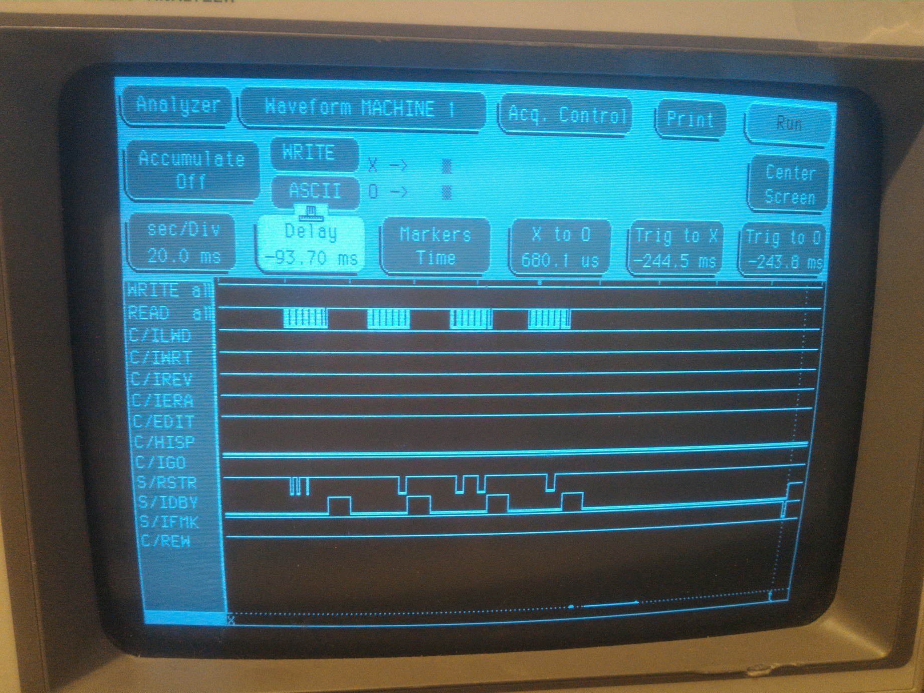
The following data analysis shows what is happening during a "READ" signal - one sort pulse of /IGO.
Assuming the tape is online (IONL = 0V) and ready (IRDY = 0V), the controller pulses "IGO". At startup, the drive drops IFBY (0V) and after the reels reach the operational speed, IDBY is dropped (0V). When data is ready on the bus, /IRSTR drops for a short time (0.8 uS). After 1.2uS it is dropped again signaling a new data transfer (read) should be performed on the host side.
![]()
After the end of each block, IDBY goes high (+5V/false) and the drive is ready to accept a new command.
![]()
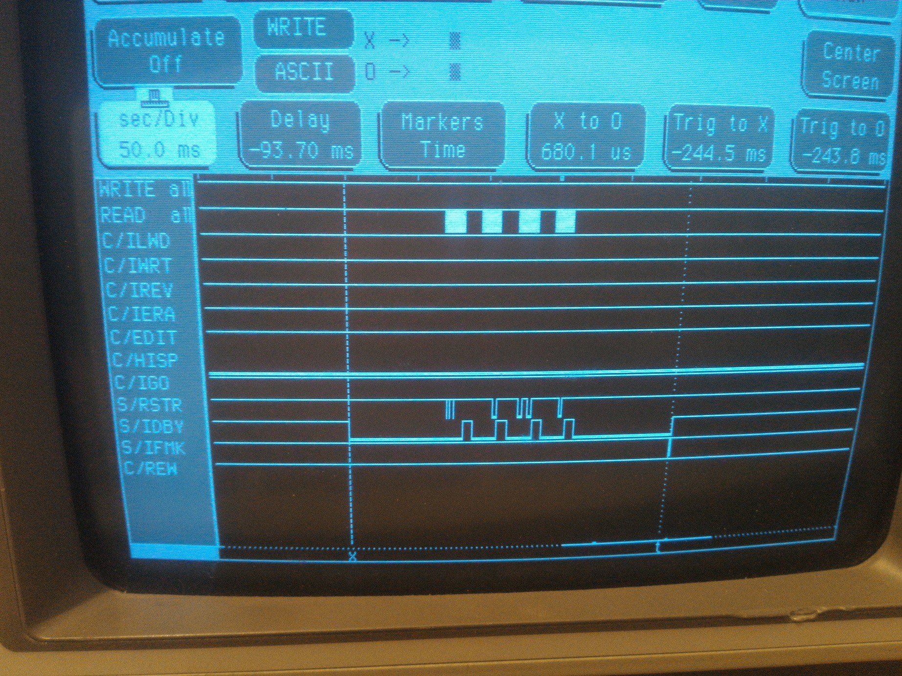
The end of a file is signaled by dropping IFMK.
![]() After IDBY raises there is a time window before IFBY also raises. This time window is used by the host to reinstruct the tape drive for a new operation. If a continuous read is desired until the end of data (2 consecutive filemarks on the tape), IGO should be pulsed during this time window. Failure to do so will cause the tape to rewind at the end of last read block, stop and wait for a new command, then start spinning the reels until operational speed is reached. This is a time consuming process and unnecessary wears the tape especially when communication is attempted on the host side without using interrupts.
After IDBY raises there is a time window before IFBY also raises. This time window is used by the host to reinstruct the tape drive for a new operation. If a continuous read is desired until the end of data (2 consecutive filemarks on the tape), IGO should be pulsed during this time window. Failure to do so will cause the tape to rewind at the end of last read block, stop and wait for a new command, then start spinning the reels until operational speed is reached. This is a time consuming process and unnecessary wears the tape especially when communication is attempted on the host side without using interrupts.![]()
End of data - not to be confused with IEOT (end of tape) - it is signaled by a second filemark and an empty read buffer. The drive waits for a new command. If append data is desired, the drive will be signaled to perform the following operations: rewind a block (the empty block shown above), erase the second filemark, write new stuff, write a new filemark (end of file) and a second filemark to signal <end of data>
[END OF TRANSMISSION]
-
Concept design drawings
04/19/2019 at 17:51 • 0 commentsShort as usual:
![]()
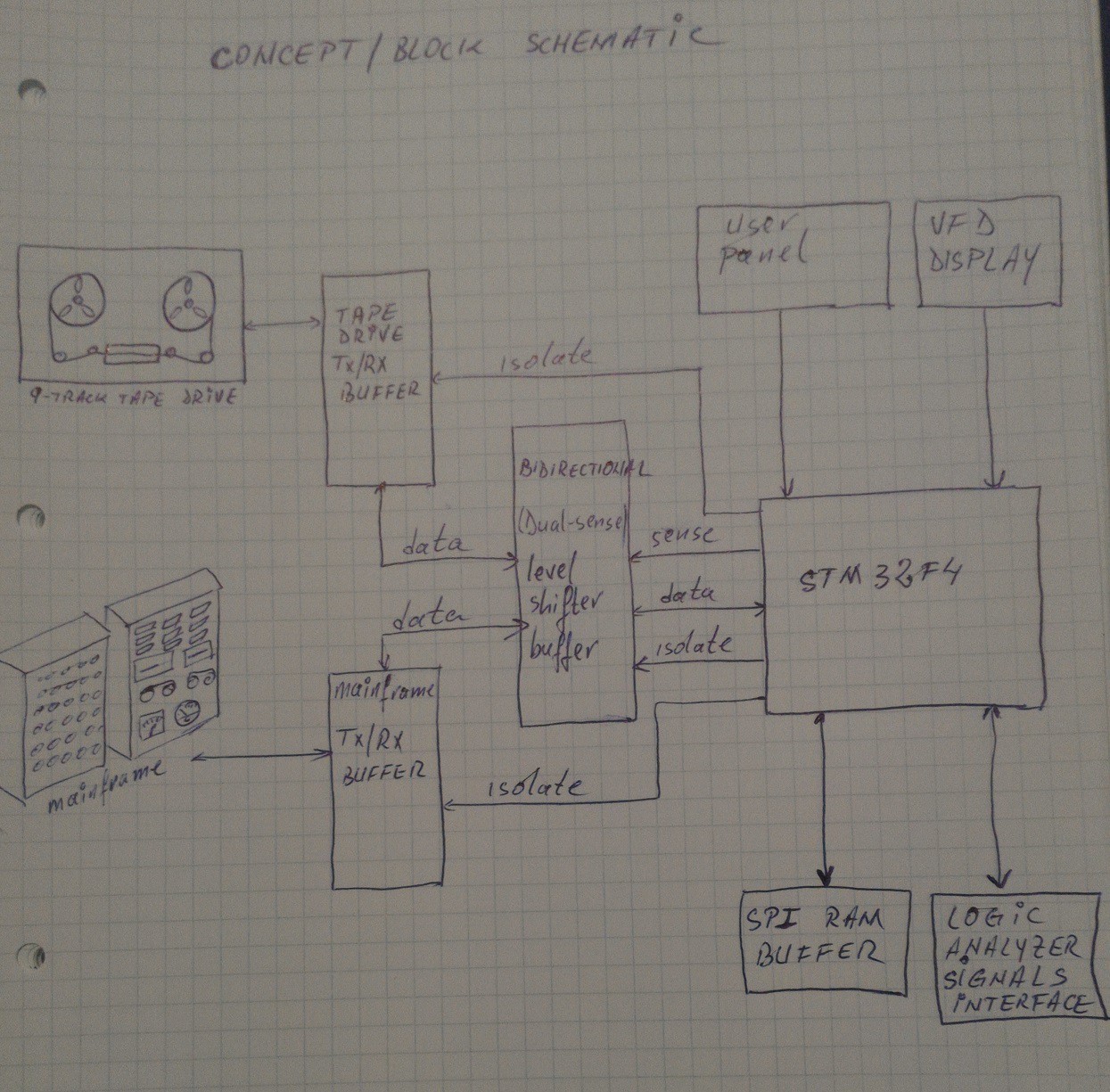
The camera is a little scratched by claws from either pussycats, bats, vampires, hedgehogs, lizards and vacuum tubes but the picture is clear enough for some explanations.
The system acts like the 'man in the middle' concept. It is connected between the tape drive and mainframe computer - one i/o buffer for each one.
The STM32 microcontroller is also connected by another bidirectional buffer which also acts as a level shifter. Datasheet for STM32F429 says the GPIOs are 5V tolerant but I do not want to risk. There is a microSD card connected to the STM32 but not shown in the schematic above.
Each buffer can be activated or switched to high impedance state - meaning the corresponding equipment is isolated.
Commands are selected from the user panel, information is displayed on the VFD and additional debugging service-mode data is available through a serialUSB line.
The following functions are supported:
1. Host mode: tape drive buffer is activated, mainframe buffer is isolated, the STM32 level shifter buffer has write+control lines as outputs and read+status lines as inputs;
2. Drive mode: tape drive buffer is switched to high impedance state as we don't need to talk to the drive. Mainframe buffer is activated and the STM32-buffer has write+control lines as inputs (accepting data) and read+status lines as outputs (transmitting data);
3. Bypass mode: tape drive and mainframe buffers are both activated and they can talk to each other while the logic analyzer is eavesdropping on the love story flowing through the data bus. The STM32 level-shifter buffer separates the microcontroller from the rest by switching to high-impedance mode.
4. Monitor/service mode: all debugging stuff is activated and slowing down the system. Either bypass, host or drive modes are monitored to help debug i/o glitches or software bugs.
Everything fits inside a 4-U rack mounted box just like this:
![]()
[END OF TRANSMISSION]
-
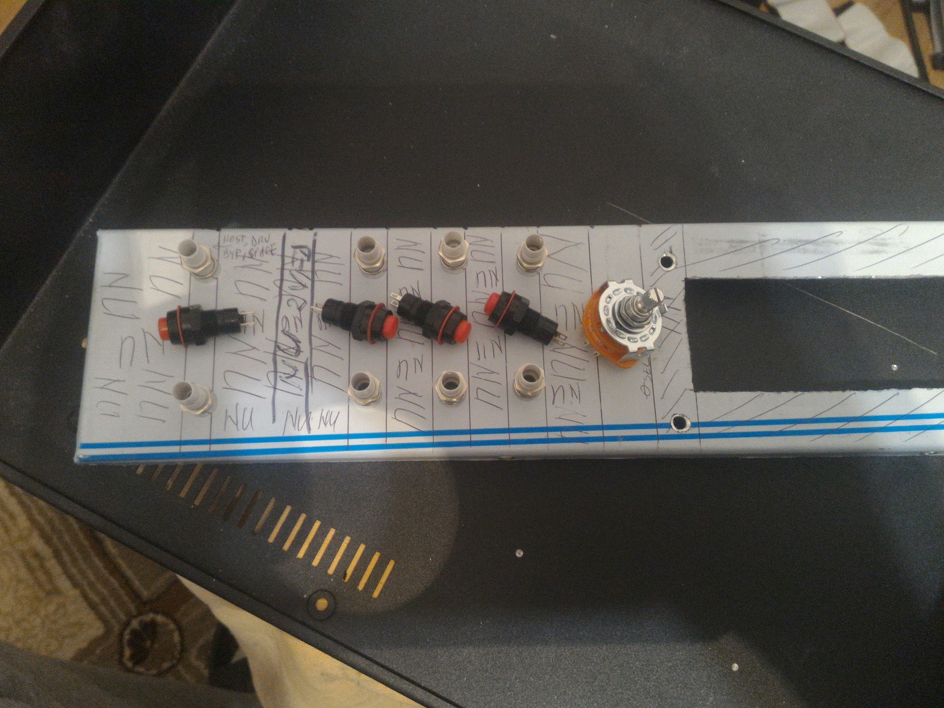
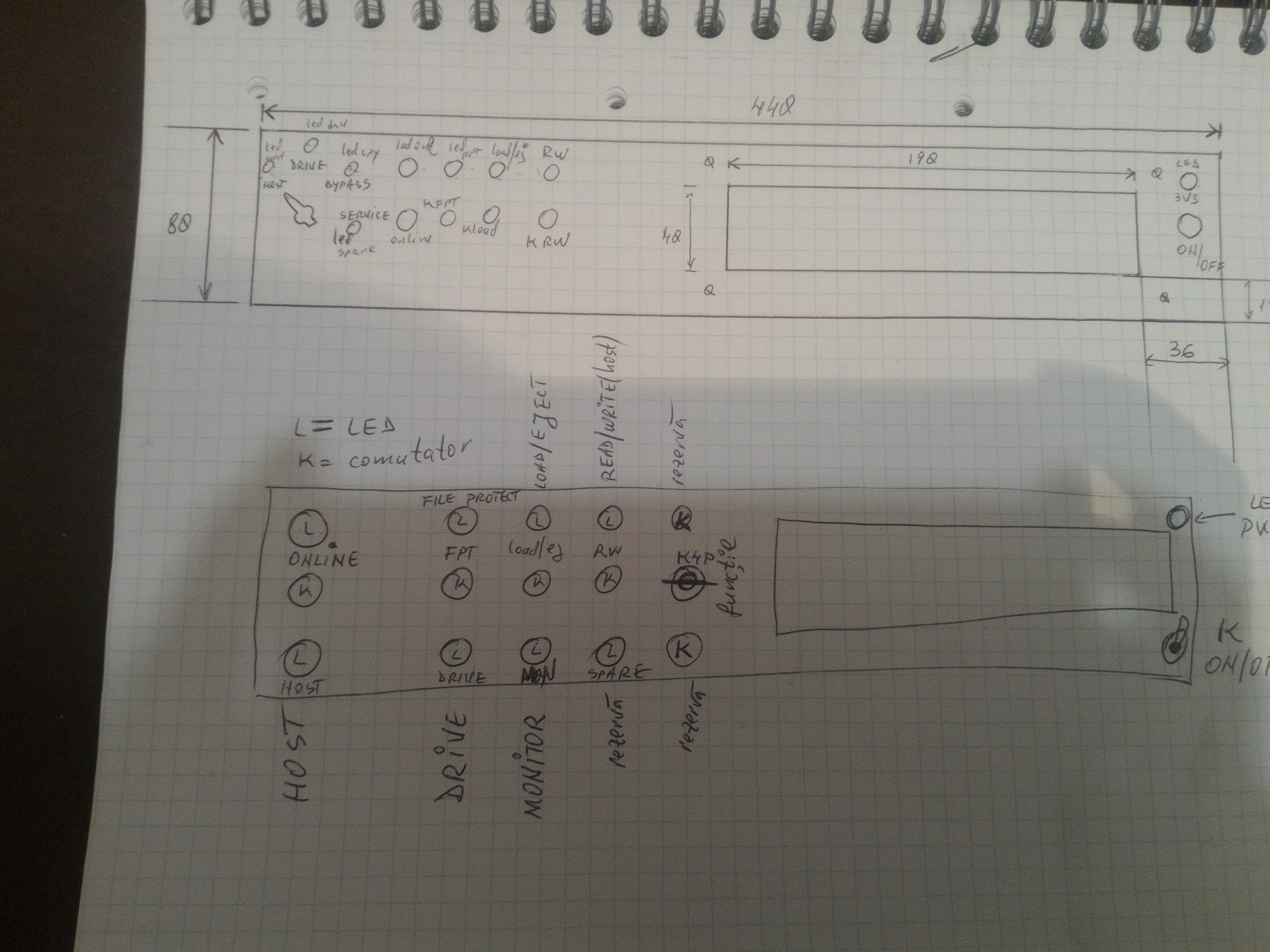
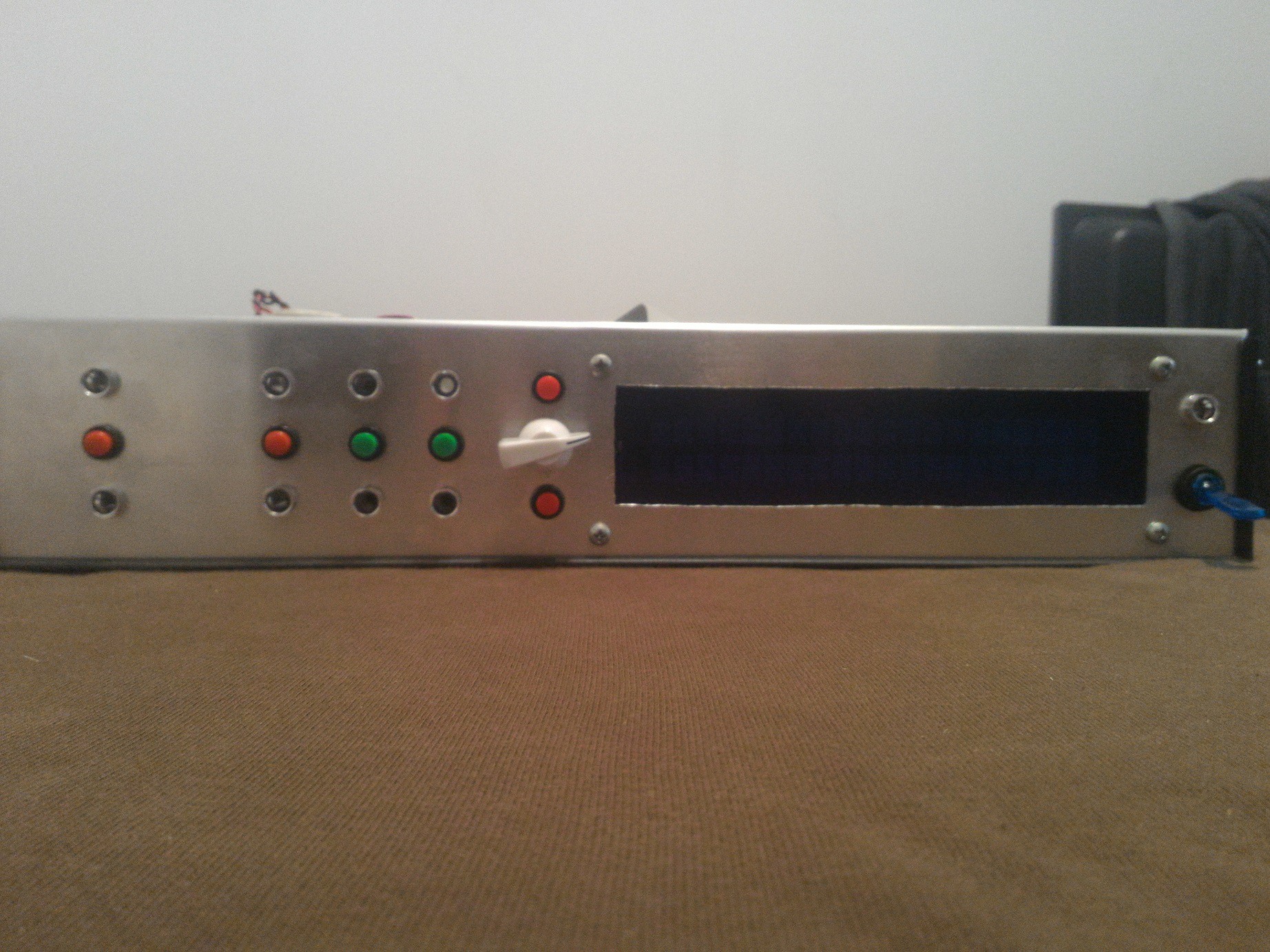
Jack in the Box
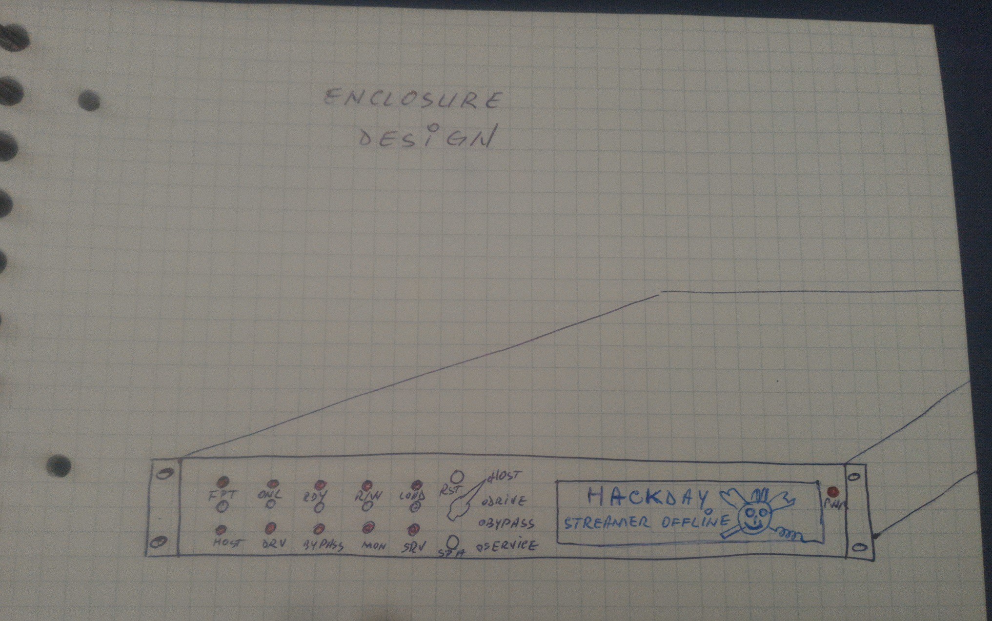
03/26/2019 at 20:29 • 1 commentAs a result of my witchcraft activity, the new experimental whispering spell needs a place to enclose its powers while performing its magic. It also needs a screen and some buttons to have fun with.
![]()
Of course the back side of the leds and buttons must not overlap the peripheral boards.
![]()
I tried many arrangements and the last one (bottom) is the final design.
Some words are in Romanian because the ancient tongue spoken by many warriors and vampires has strong magic powers especially when swearing, and spell radius&effect increase when the finest of the finest beers arrive at the local shop.
From top-left to right:
L is LED, K is button.
Online, File Protect, Load/Eject, READ/WRITE, the "K4P" means button with 4 positions which selects the functions.
Bottom leds:
Functions: Host mode, Drive mode, Monitor mode, the "spare" is now Bypass mode and the last button (K) on the right is no longer connected, just like the button above K4P.
Right side of the screen: top - power-on LED, bottom - on/off switch.
![]()
![]()
Not bad for a manually processed 4U rack-mounted enclosure. The brackets are not installed yet.
![]()
Both mainframe and tape drive need two connectors. This is the Pertec interface: the greatest pain of the PDP-era. There is no acknowledgement between the host and the drive. The data is just.... "roared" through the bus and the circus training is performed using status and control line jugglery. On software side there's a lot of logic operations - a great exercise for the neurons.
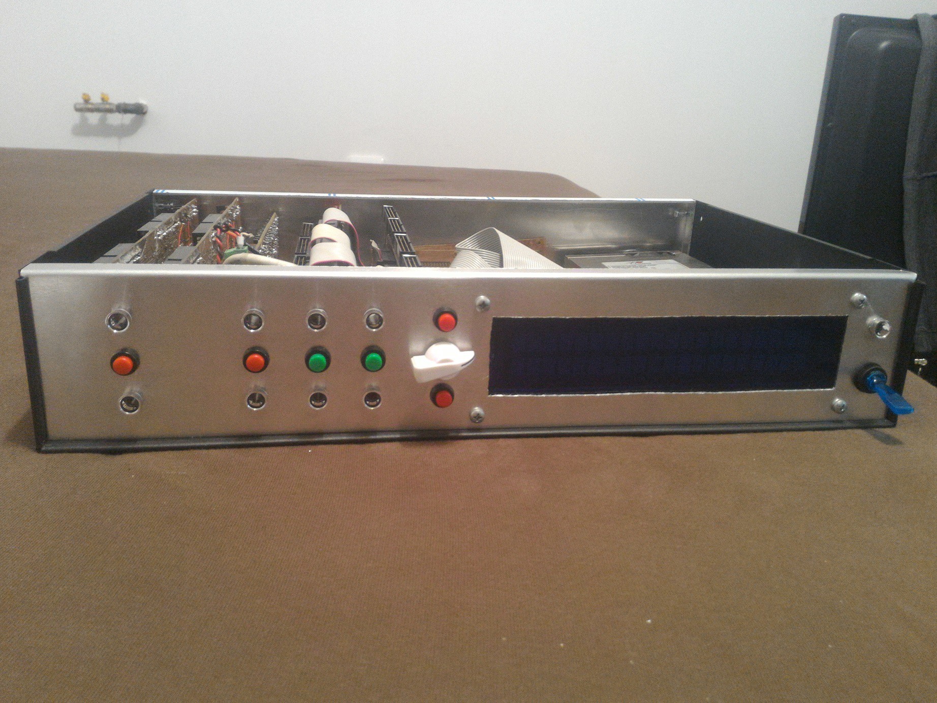
Pictures from inside:
![]()
![]()
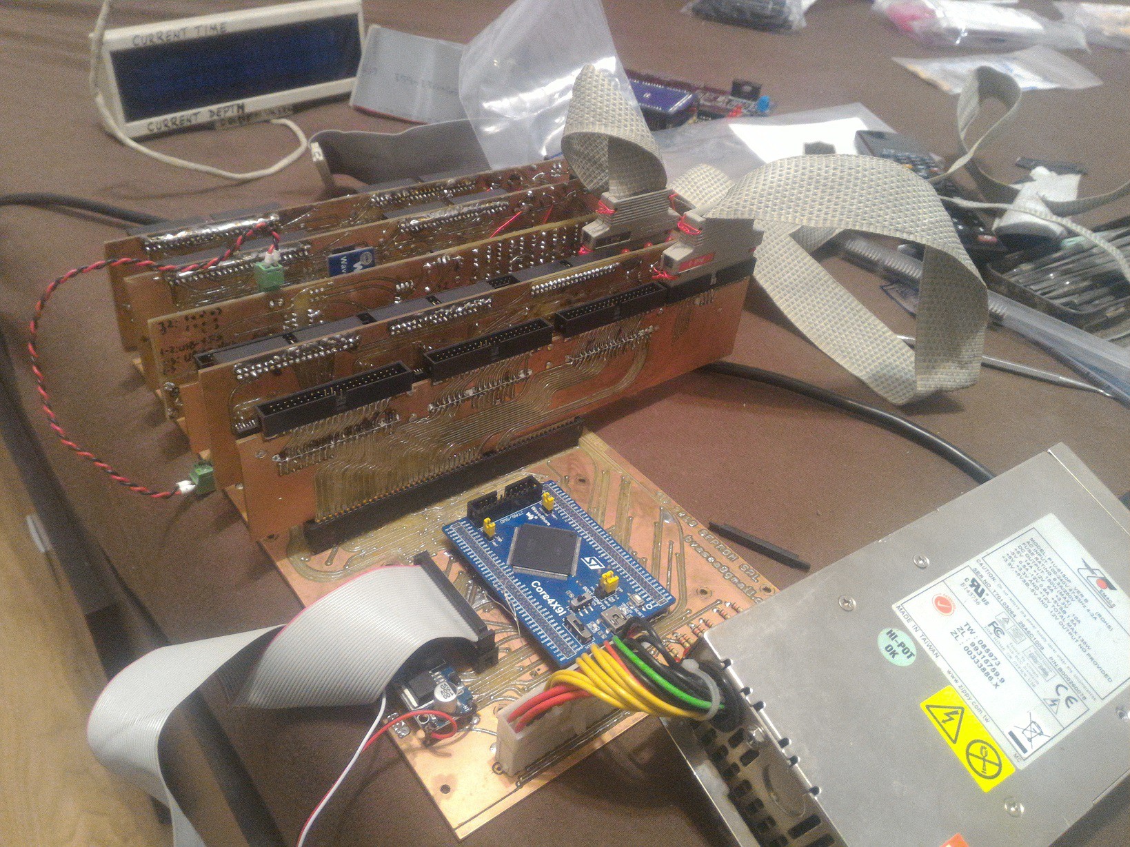
from left to right:
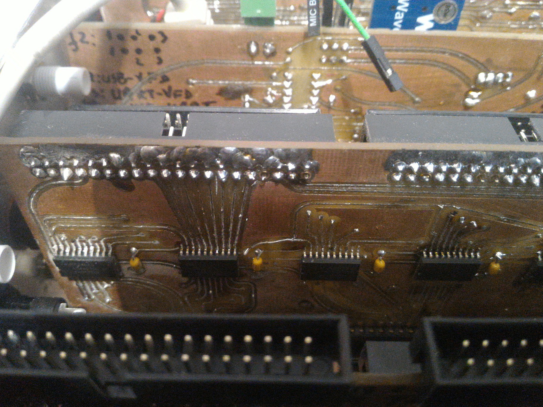
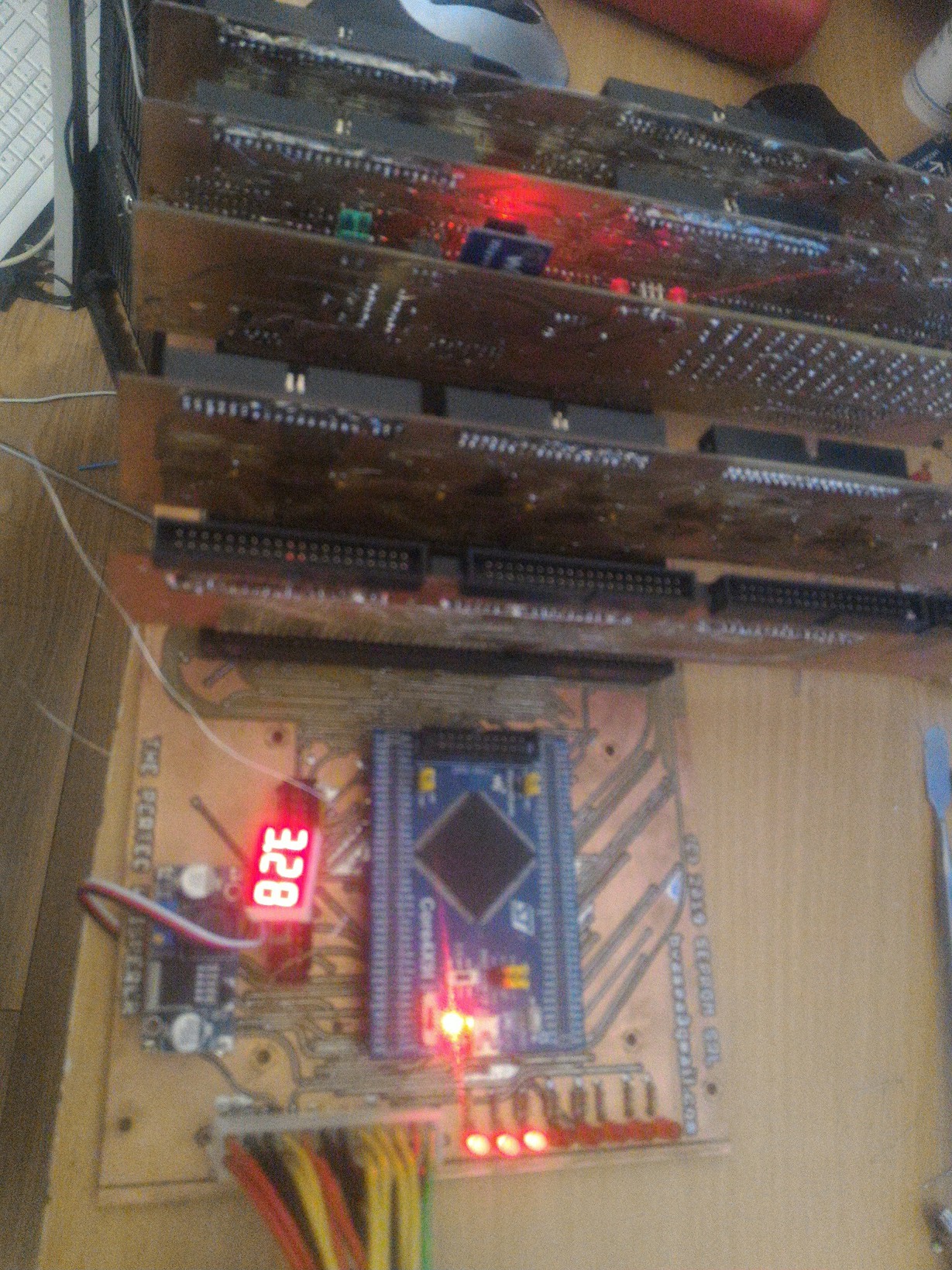
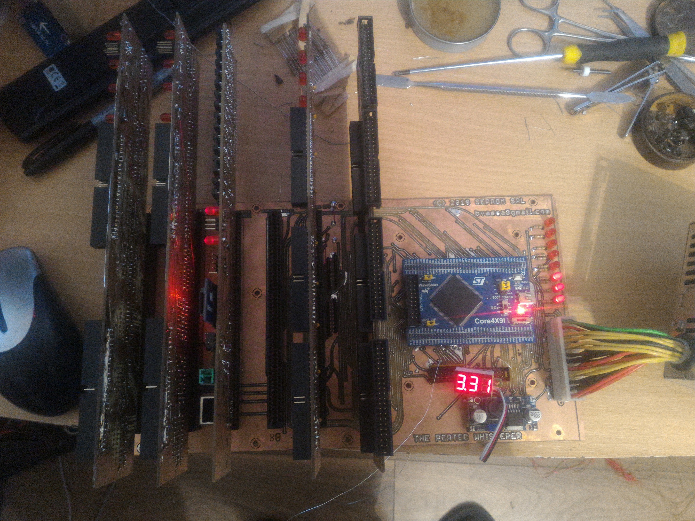
ATX PSU, STM32F4 CPU board, CPU interface to buffer (has 4 x IDC40 connectors on top), CPU Buffer, Bus interceptor (4 x IDC40 on top), rambuff+comms, mainframe buffer, tape drive buffer.
![]()
![]() Display via an old POS 2x20 VFD with 9600 baud serial line.
Display via an old POS 2x20 VFD with 9600 baud serial line.![]()
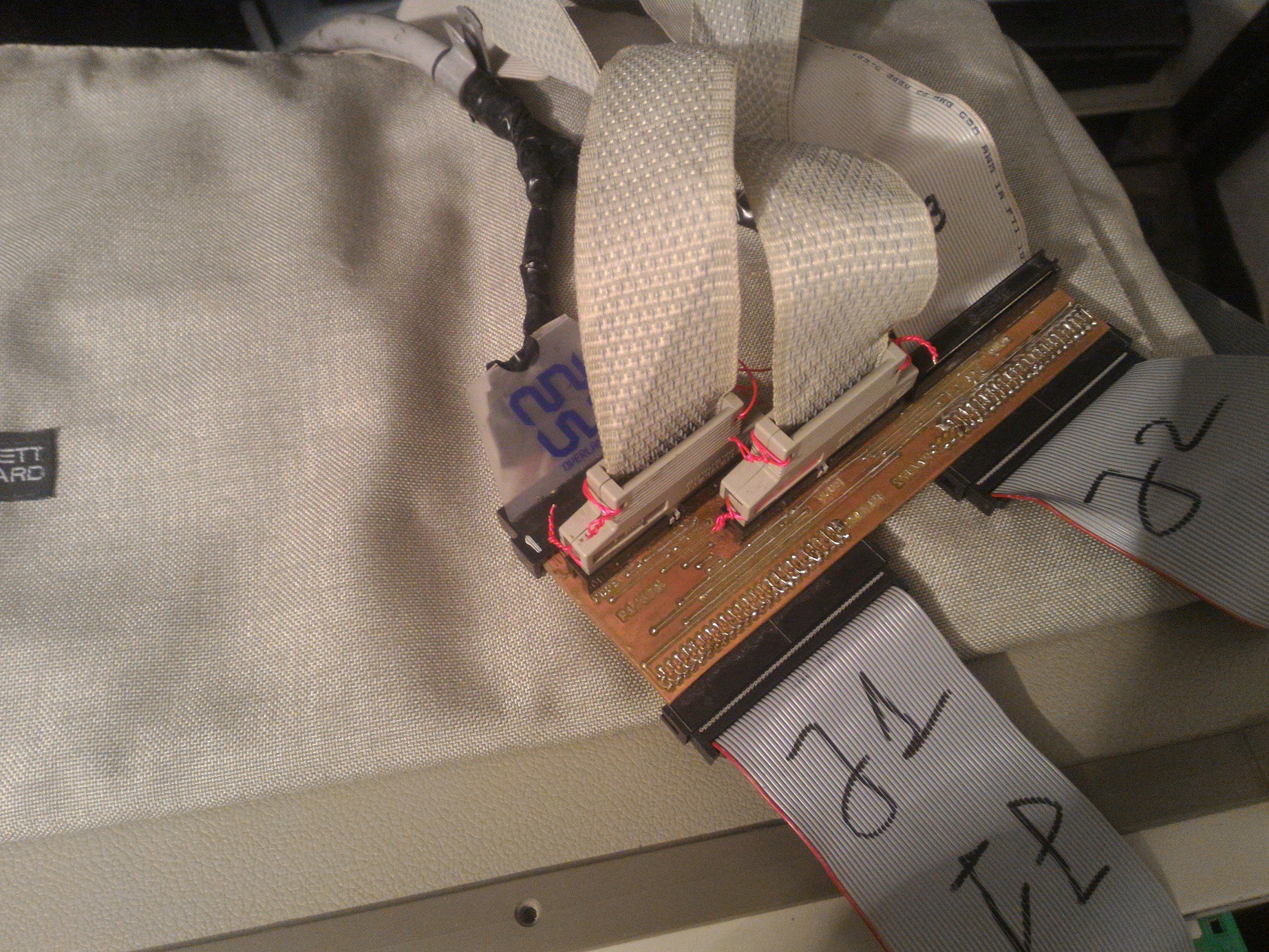
The edge-mounted IDC40M connectors helps me watch the magic flow using the HP1662 logic analyzer.
![]()
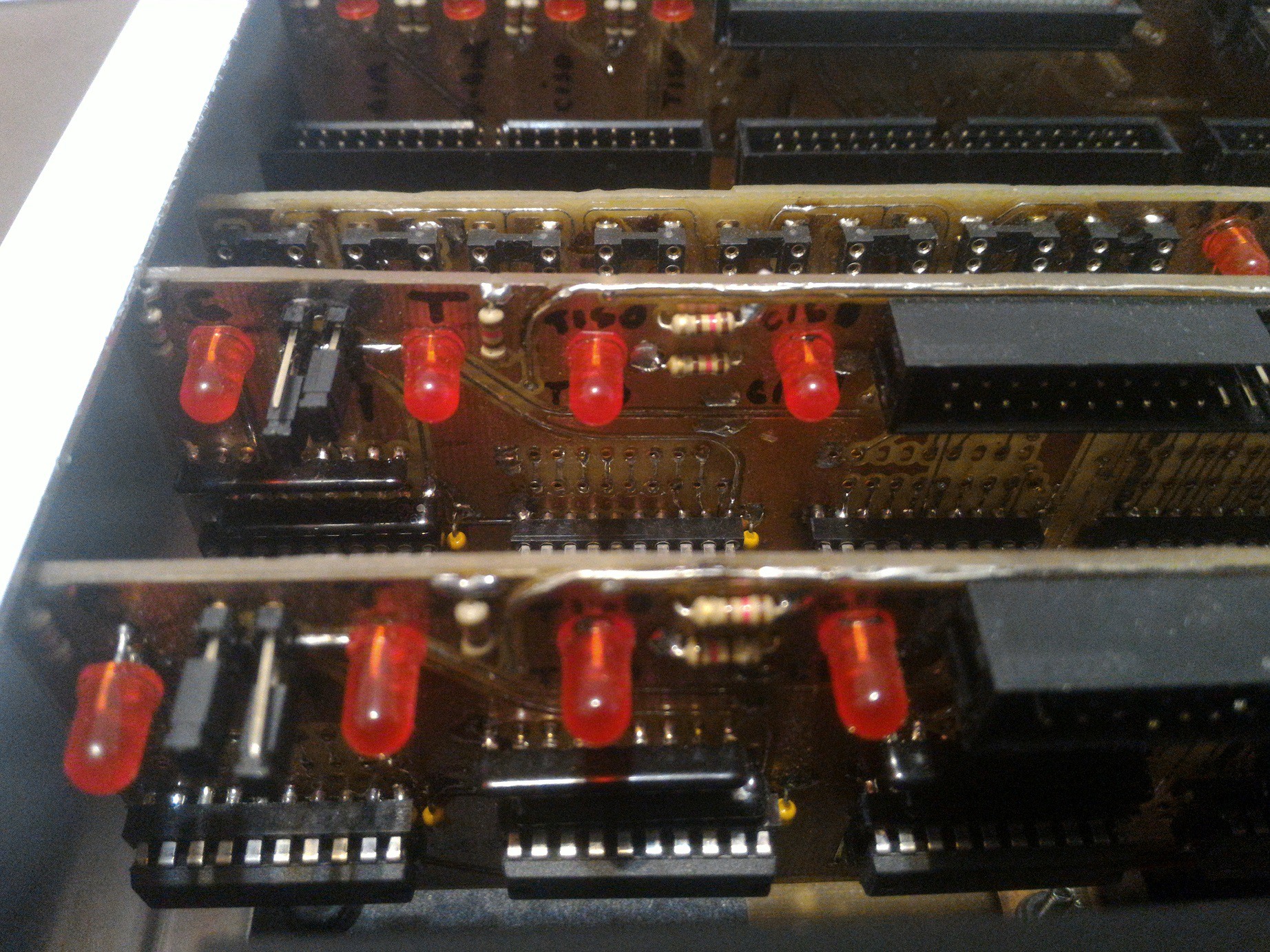
TISO: tape isolate; CISO: controller (mainframe) isolate.
![]()
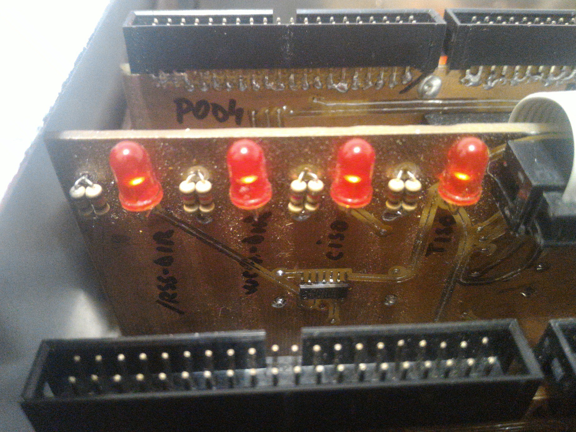
/RSS-DIR: Read-StatuS direction - it changes between host and drive mode;
WCA-DIR: Write-Control-Address direction - also changes like above.
![]()
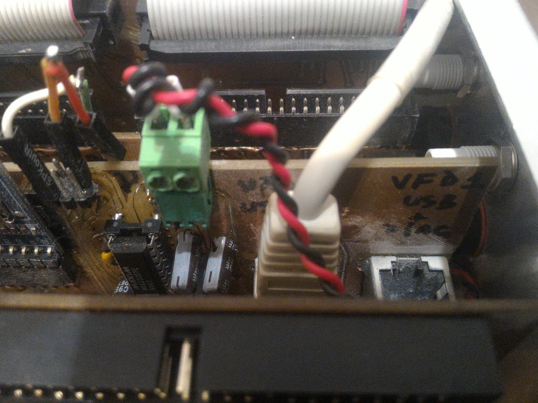
Close-up view of uSD card module, the MAX232 and the RJ45 serial VFD connector
![]()
![]()
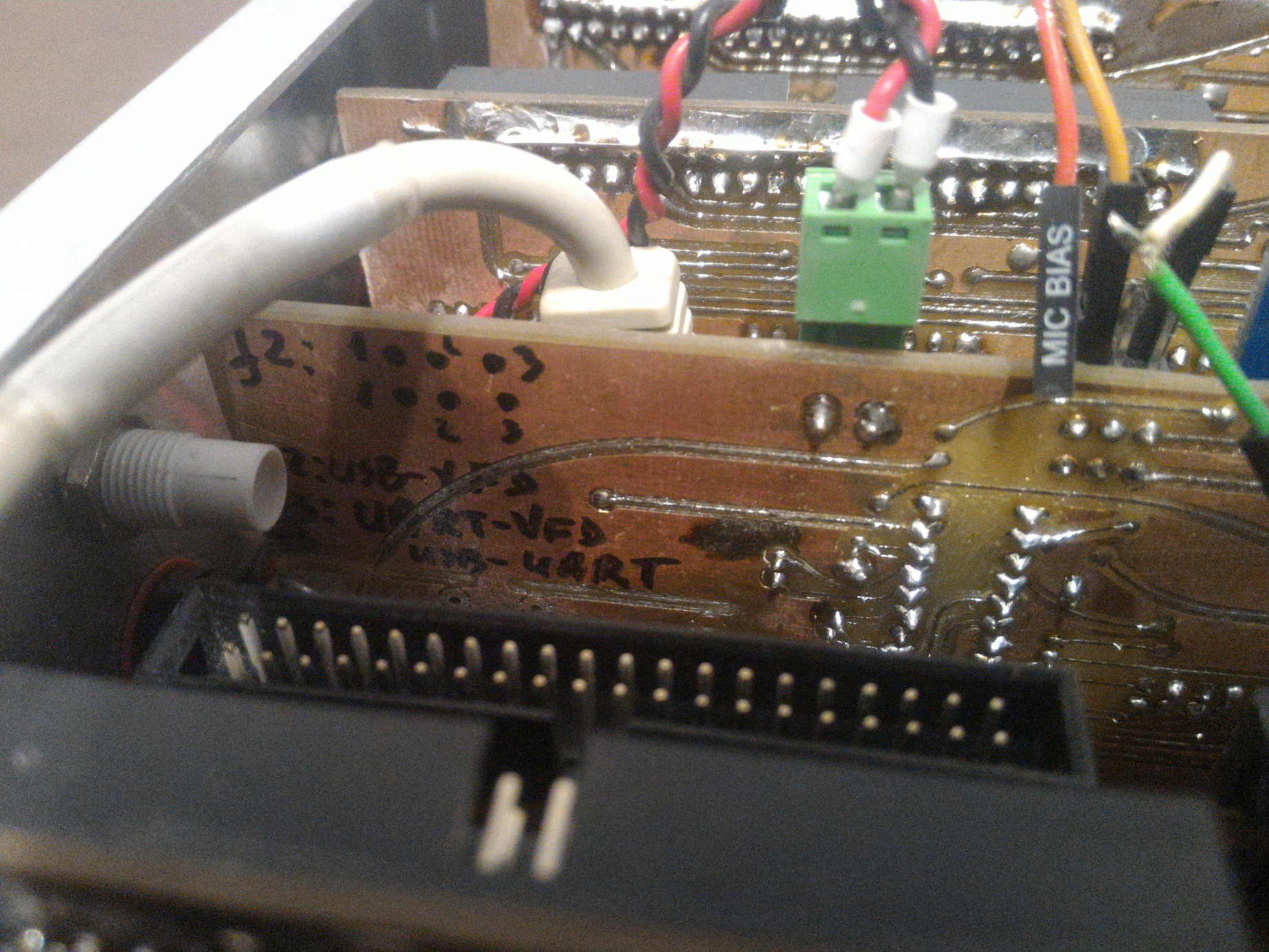
There is a second RJ45F on the board. The second VFD is used as a debug console when I am too lazy to connect the serial line to another PC.
![]()
![]()
Close view of the micro controller i/o buffer. This is bidirectional and it also serves as a 5V to 3.3V level shifter.
![]()
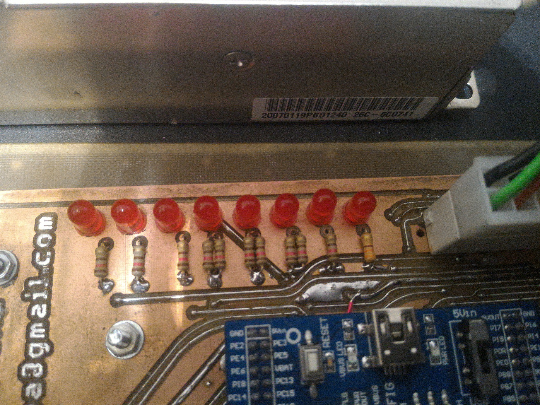
Status leds. From left to right:
mainframe_isolate, rss_dir, wca_dir, tiso, ciso, 3v3, 5V, 12V.
![]()
![]()
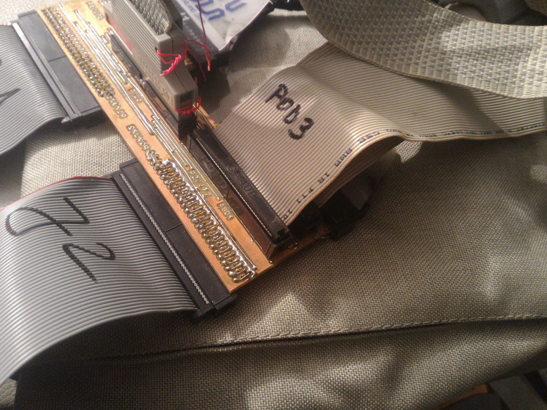
This is the pertec interface interceptor from the controller (mainframe) side of the Whisperer. In the back side there are two card-edge-50 connectors, that's the input. The J1 and J2 outputs go to the 'mainframe' connector shown in the 5th picture.
You can also notice the 4 x IDC40M connectors. With them I can inspect the traffic using the HP1662 analyzer at input, inside the system and there is also another pertec interceptor at the output. This way I can trace any operation failures.
Party time!
![]()
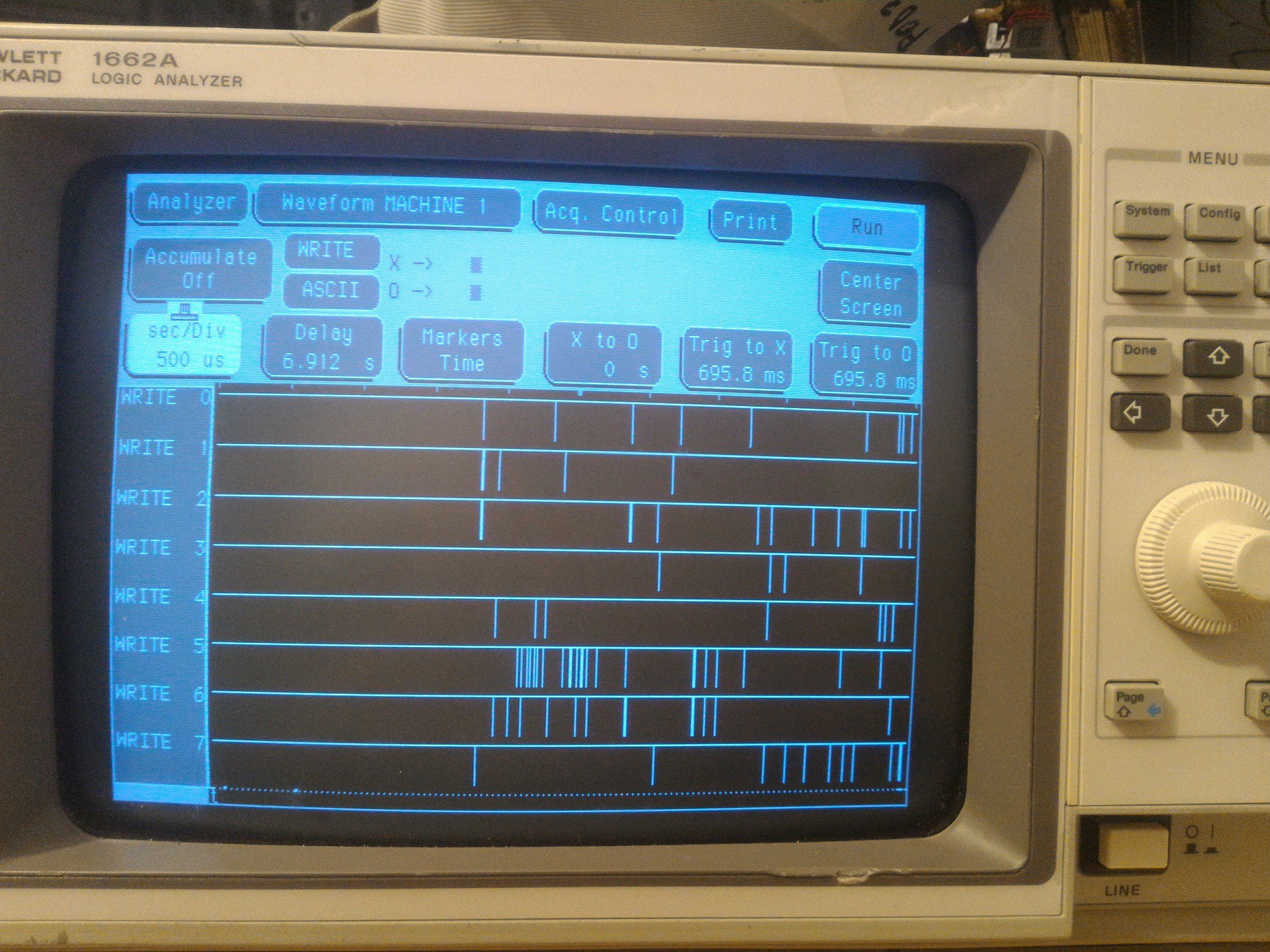
The analyzer pods are shown here. Whatever line is up, it means logic 1. Down is logic 0.
The Pertec interface use inverted logic, meaning a drop of voltage means true.... and from now on it is extremely important what kind of beer I chose in order to see the true data in the inverted flow.
![]()
This old beast has a beautiful manual with a lot of pages showing the complex operations for programming whatever I want to analyze.
![]()
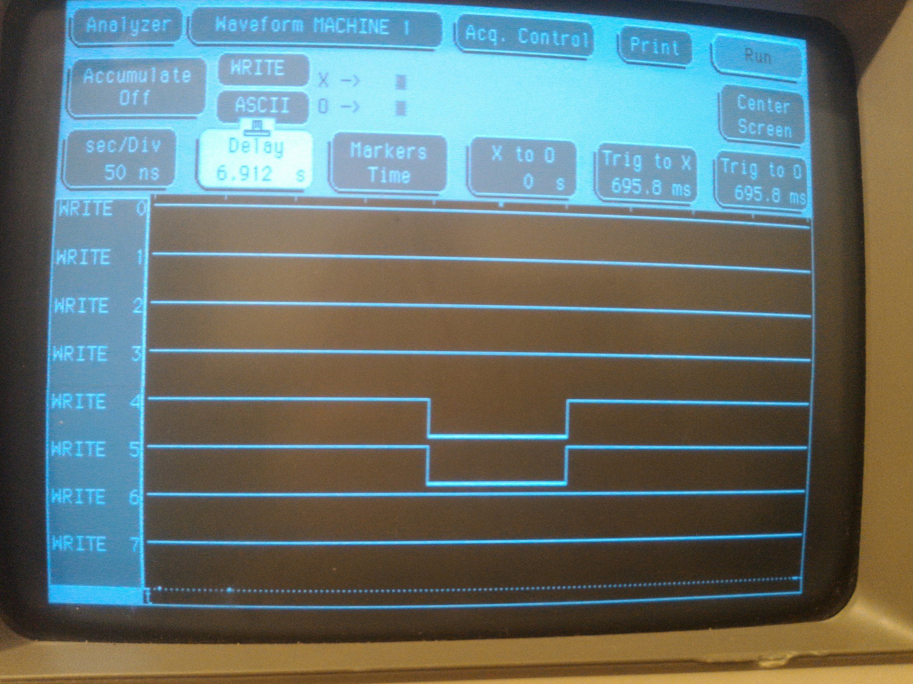
This has not been seen for decades - the actual flow of a Pertec interface data transfer.
![]()
W0......W7 lines during a "tar -cvf /dev/nsa0 /etc" operation.
![]()
"nsa0" was achieved under FreeBSD 11.3 and an old Pertec to SCSI converter from Qualstar.
![]()
![]()
This is the place where tie magic happens.
[END OF TRANSMISSION]
-
It's alive!!
02/20/2019 at 20:21 • 2 commentsMy Frankenstein motherboard just completed its first test - serial RS232 data transfer at 9600 baud to the VFD Display.
![]()
![]()
![]()
![]()
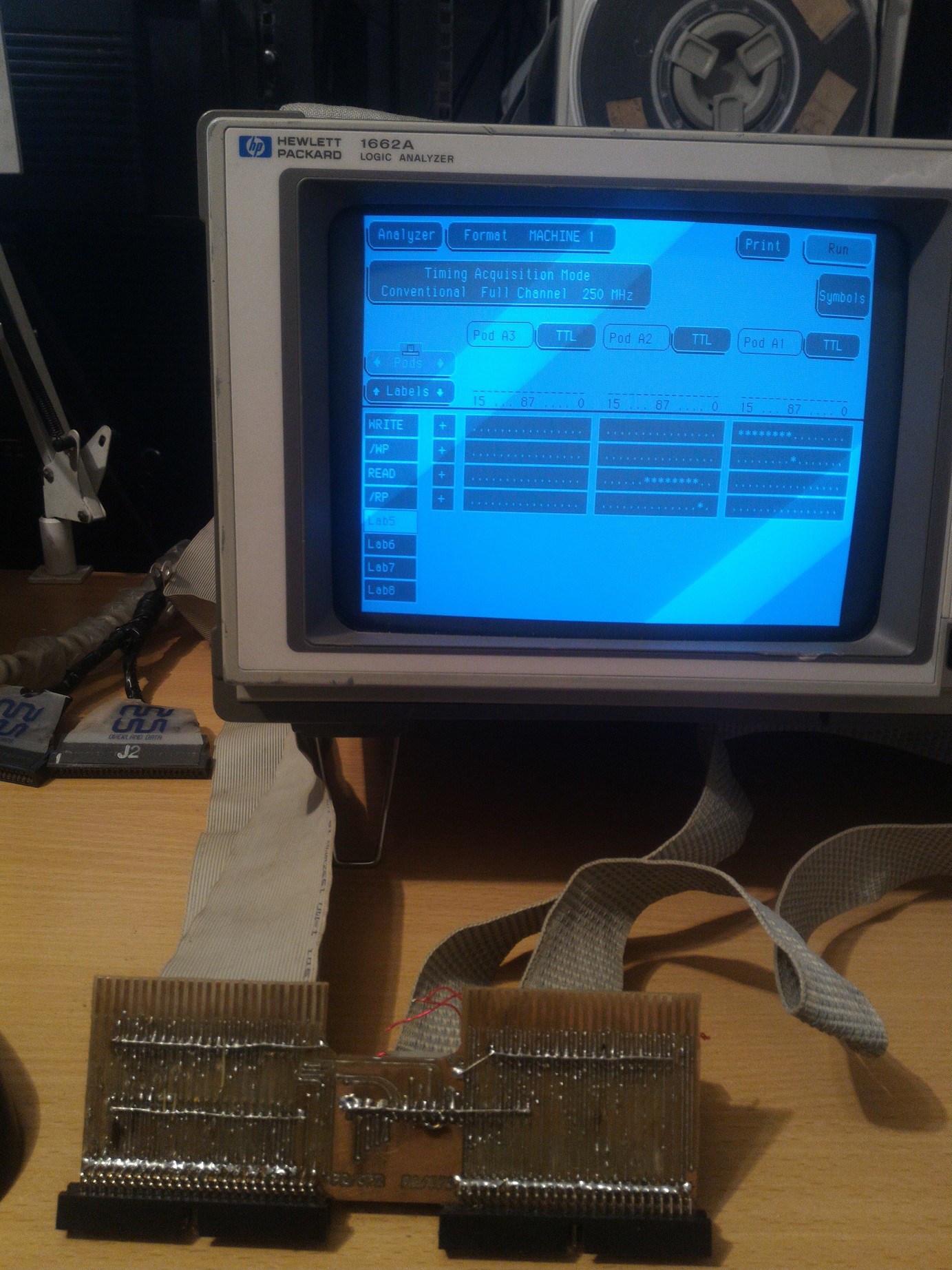
A friend sold me a HP 1662 logic analyzer with one of the probing cable missing, so I built an adapter. All those vertical IDC40-M connectors you see on top of the peripheral boards will go to this logic analyzer.
![]()
![]()
![]()
In the mean time I am preparing the box where all this frankenmonster will stay hidden.
-
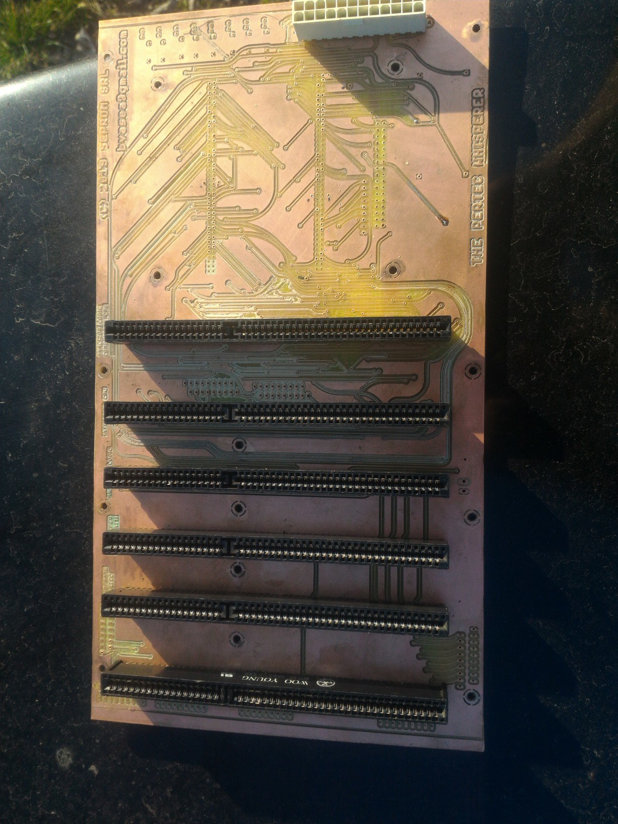
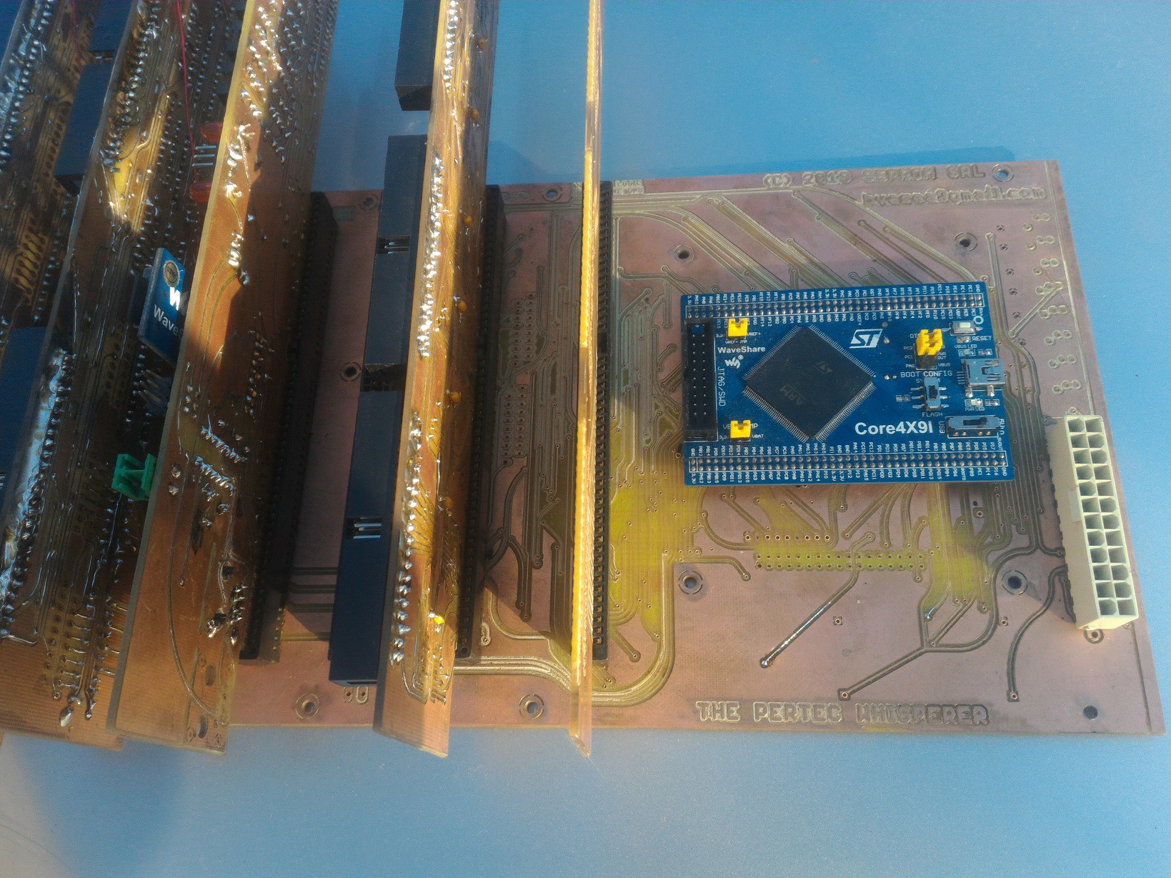
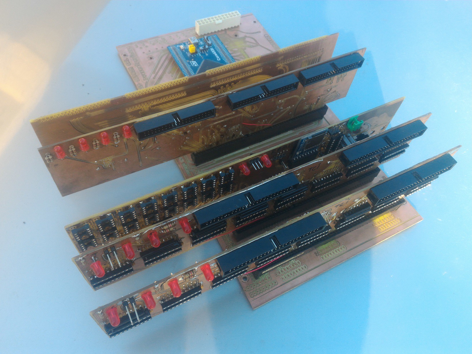
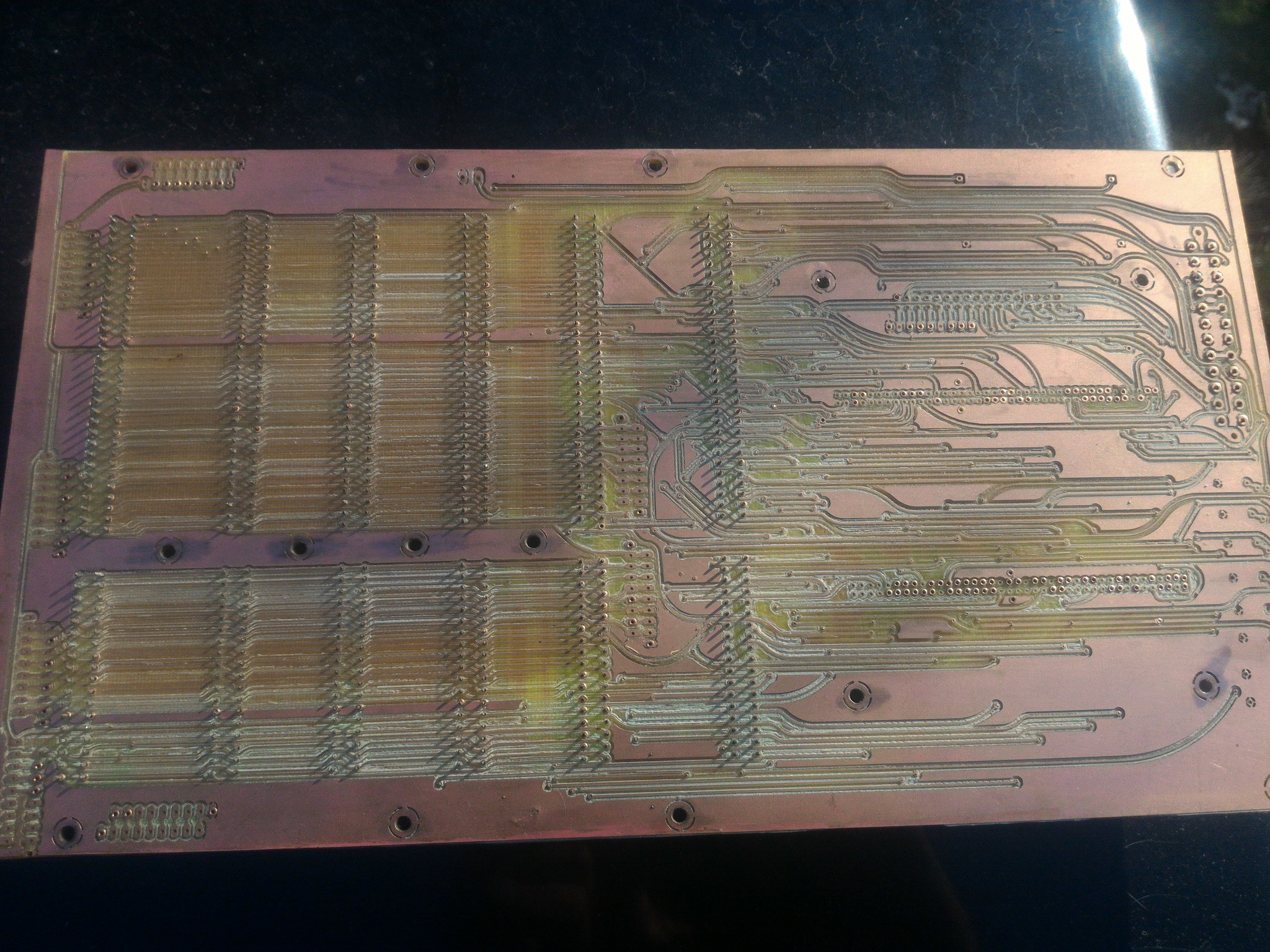
The Main Board (II)
02/17/2019 at 21:27 • 2 commentsWork in progress - I have to check and re-check every pad, every hole, every piece of circuit because my CNC is old and its work is far from perfection.
![]()
![]()
![]()
![]()
![]()
![]()
![]()
THE PERTEC WHISPERER-MAINFRAME TAPE DRIVE EMULATOR
A.K.A. THE 9 TRACK TAPE DRIVE COMMUNICATOR Talking to Mainframes Era Reel to Reel 9 track tape drives
 After IDBY raises there is a time window before IFBY also raises. This time window is used by the host to reinstruct the tape drive for a new operation. If a continuous read is desired until the end of data (2 consecutive filemarks on the tape), IGO should be pulsed during this time window. Failure to do so will cause the tape to rewind at the end of last read block, stop and wait for a new command, then start spinning the reels until operational speed is reached. This is a time consuming process and unnecessary wears the tape especially when communication is attempted on the host side without using interrupts.
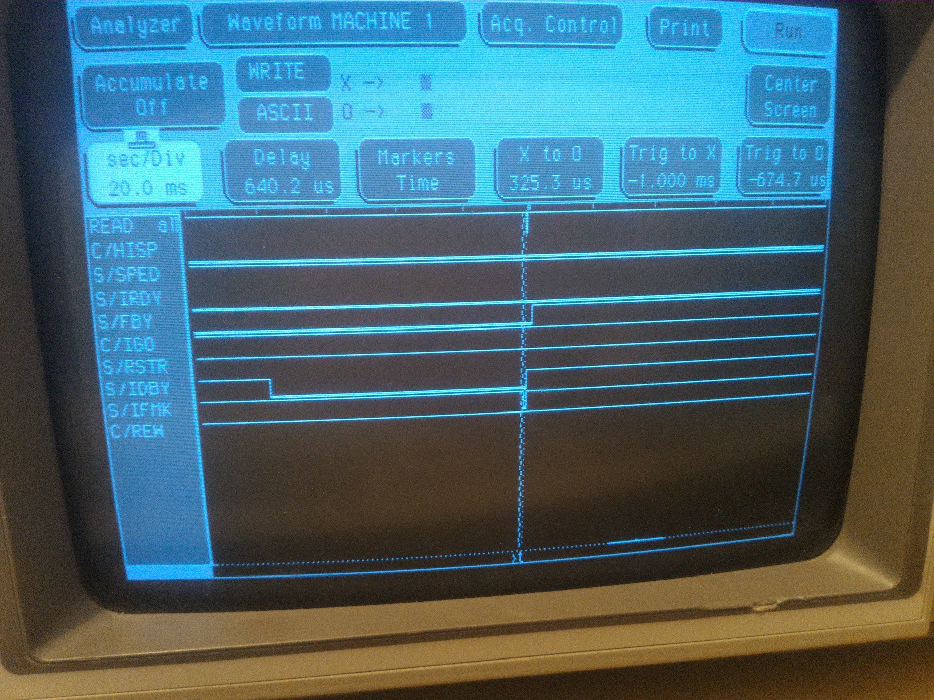

 Display via an old POS 2x20 VFD with 9600 baud serial line.
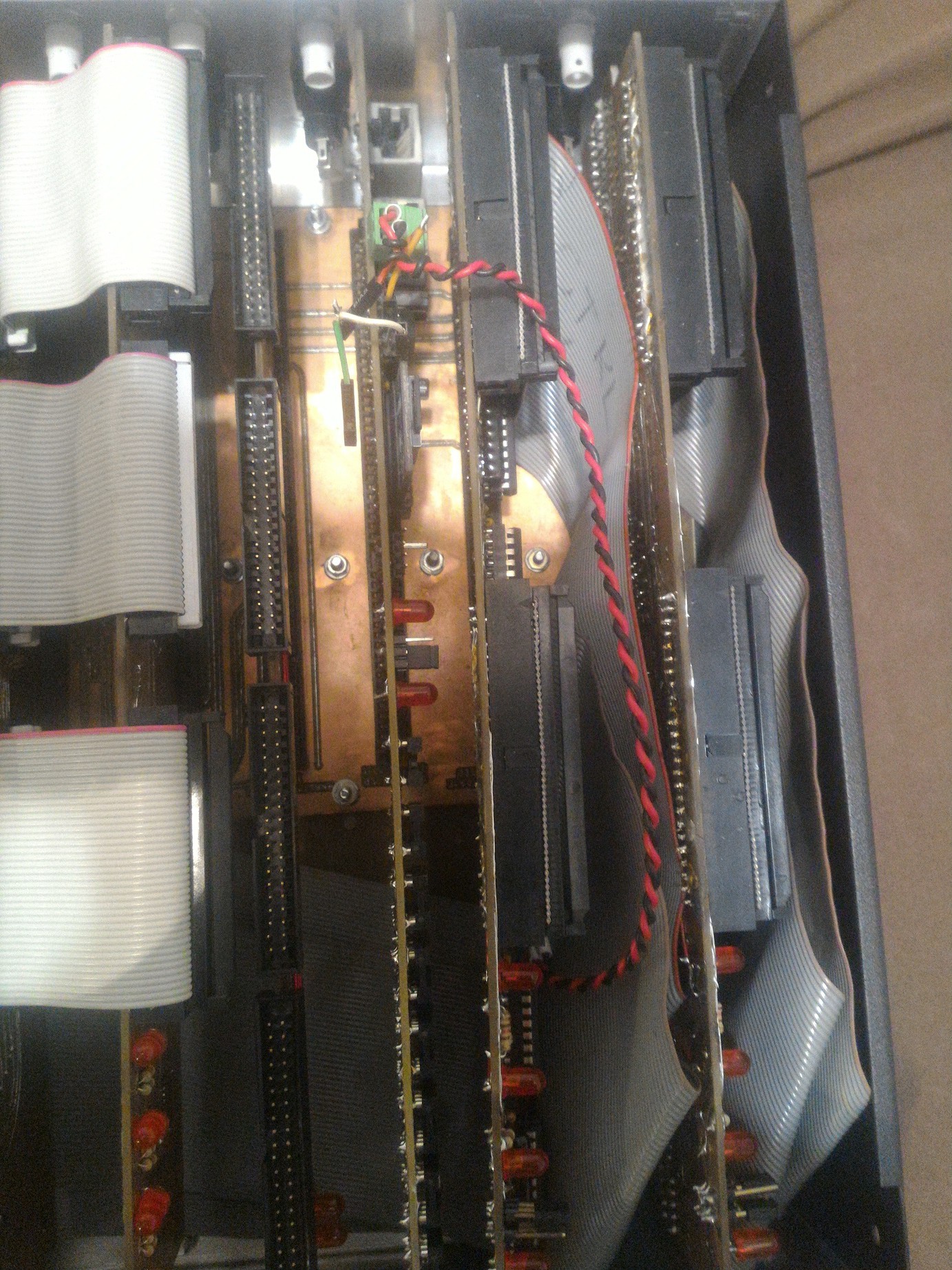


