To make the experience fit your profile, pick a username and tell us what interests you.
We found and based on your interests.
ddl4-clock-revB1.pdfPDF Schematic for Clock Generator Module - Copyright (C) 2018, David Anders. All Rights Reserved.Adobe Portable Document Format - 18.31 kB - 07/01/2018 at 20:58 |
|
|
ddl4-pc-ir-revB1.pdfPDF Schematic for Program Counter and Instruction Register Module - Copyright (C) 2018, David Anders. All Rights Reserved.Adobe Portable Document Format - 28.28 kB - 07/01/2018 at 20:55 |
|
|
ddl4-rom-revB.pdfPDF Schematic for ROM Module - Copyright (C) 2018, David Anders. All Rights Reserved.Adobe Portable Document Format - 13.30 kB - 06/29/2018 at 03:55 |
|
|
ddl4-registers-revB.pdfPDF Schematic for Registers Module - Copyright (C) 2018, David Anders. All Rights Reserved.Adobe Portable Document Format - 33.34 kB - 06/29/2018 at 03:55 |
|
|
ddl4-ram-revB.pdfPDF Schematic for RAM Module - Copyright (C) 2018, David Anders. All Rights Reserved.Adobe Portable Document Format - 22.07 kB - 06/29/2018 at 03:55 |
|
|
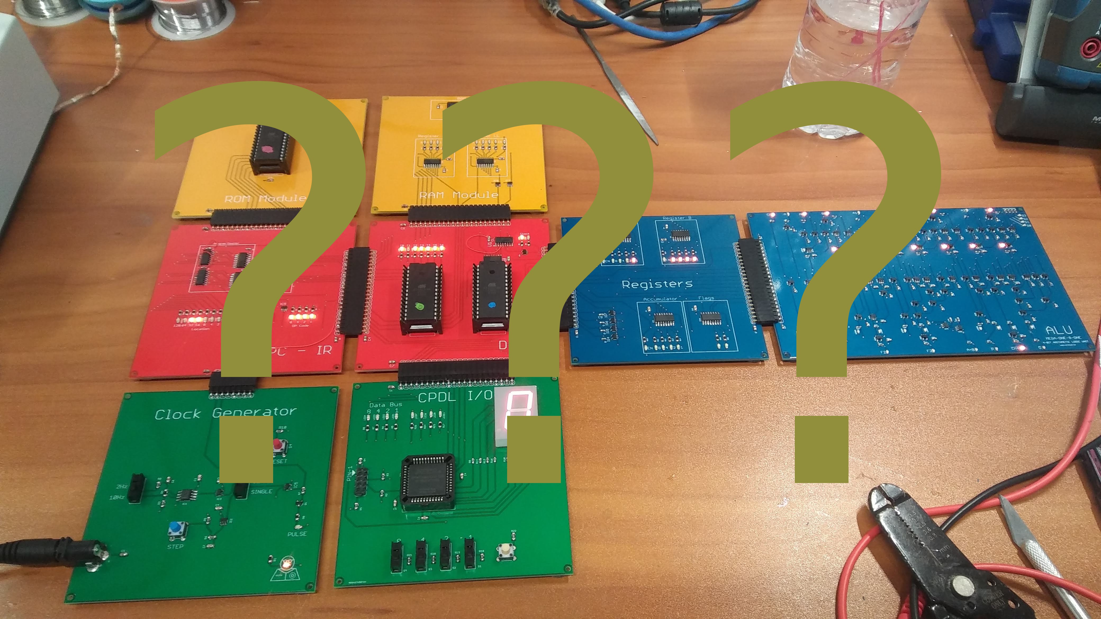
So with the second revision of the DDL4-CPU complete and functional, all my personal objectives have been met with this project. Even thought I did get some coverage from Hackaday.com and Hackster.io , I got very little direct feedback or interaction for the project, so I am wondering where to go from here with the project... thoughts anyone? Bueller? Bueller? Bueller?.......
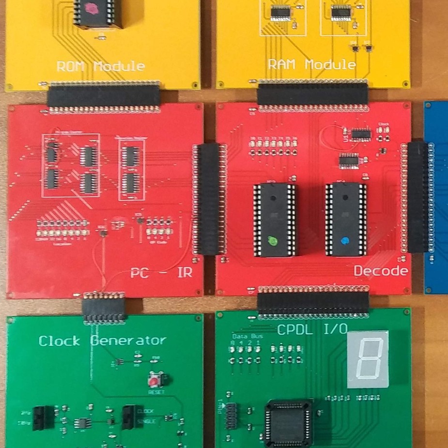
In the first revision of the DDL4-CPU, the Clock Generator Module connects to the Program Counter / Instruction Register (PC/IR) Module via a single row 8 pin header. Only 5 signals are used out of the 8. I left room for expansion and testing. The rest of the modules are connected together with a single row 22 pin header. The pinout of the header varies a little between board but there is a loose format to the pinout:
1 - VCC
2-9 DATA_BUS[8:0]
10-19 Control Signals
20 - Reset
21 - Master Clock
22 - GND
While the Clock Generator Module only needs 5 pins, it is the one module that I didn't use the 1x22 header, and to be perfectly honest, it looks out of place. The 1x8 header that it currently use is more than enough, however it just "looks" out of place, so for consistency and pure aesthetics, I am replacing it with the 1x22 header on revB of the design...
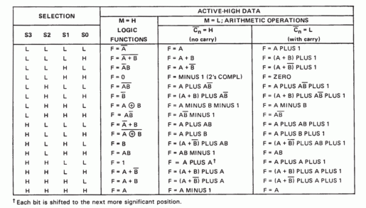
The Mega-One-8-One ALU used in the DDL4-CPU is a gate level replica of the 74181 ALU. The 74181 actually support two modes of operation. The first being a "MATH Mode". When the Mode pin is set low, The ALU can perform 16 specific math functions. When the Mode pin is set high, then the ALU is in "LOGIC Mode". In this mode, there are 16 separate bitwise logic functions that can be performed. Due to the number of op codes being limited to 16 on this design, I had initially made the decision to not add an op code for the "LOGIC Mode". The initial Instruction Set Architecture (ISA) that I had created only included the Math functions with carry and without (see All Your ISA Belong to Me!). After doing the first revision on the design, I came to the conclusion that the jump and jump with flags could be optimized reducing the number of jump commands from 3 to 1 ( see Masking Jump Requests). This freed up two operation codes (OP code), one of which could be used for the ALU logic functions. However, I ran into another problem. Every single pin of my dual EEPROM microcode was being used. If I wanted to support the ALU logic functions, I would need to decode them outside of the EEPROM microcode, similar to what I had done with the jump and jump with flags. I needed a way to easily decode 3 OP codes:
MWC - Math With Carry
MNC - Math No Carry
LOG - Logic Function
The solution actually turned out to be simpler than I had expected. By reorganizing the ISA OP codes, I was able to place the ALU functions as the first three ops codes:
This meant that for MWC and MNC, the first three binary digits were zeros. All other combinations of OP codes would not have the first three binary digits as zero. This provides a simple clean way of decoding with a 3-input OR gate. Since I am already using 2-input OR gates on the design it was easier to just implement the 3-input OR gate with two 2-input OR gates:
This simple hardware solution has expanded the capabilities of the DDL4-CPU tremendously by add 16 new logic functions. Of course, as a hardware decode solution, it has trade-offs as compared to implementing it in microcode. With microcode, if I want to change the overall design, I simply flash it with new microcode. If I want to change this ALU Mode implementation, it has to be done with new hardware. This has implications for real world problems such as those with the recently discovered CPU bugs Meltdown and Spectre. Since the core issue of these bugs are part of the physical hardware implementation, and not part of the microcode, they can't be easily fixed by producing new microcode.
As a side note, as I am working through these issues of optimization of the design, I've had a strong sense of connection with those pioneers of the 1970's and 1980's creating new microprocessor and microcontroller architectures. I now understand a lot more about how and why these developers went to such great lengths to "save one signal" or optimize their ISA with "weird" commands and groupings....
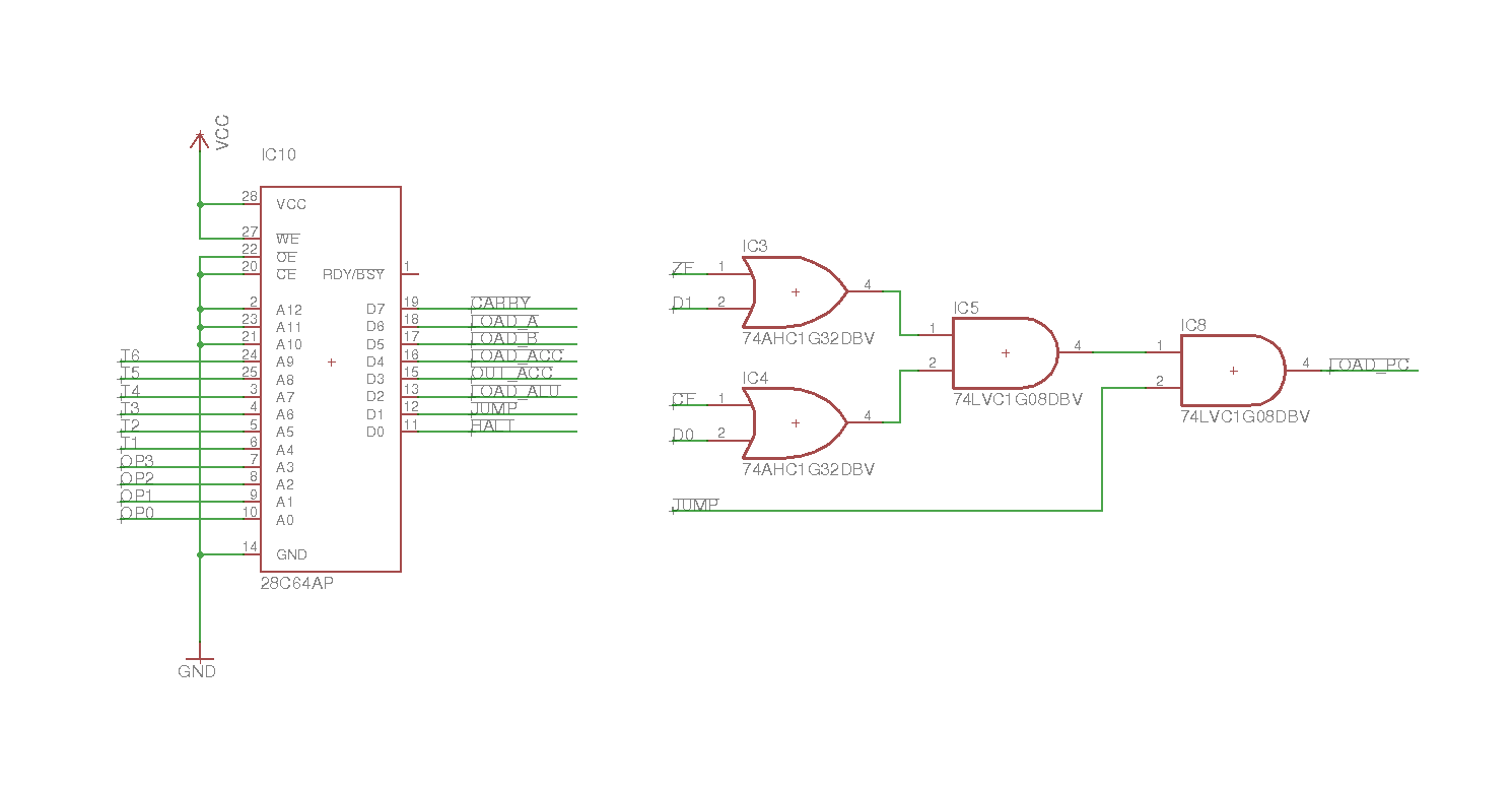
As discussed in the earlier post (Let Me Look That Up For You!), my initial implementation for conditional jumps was not a robust solution creating a lot more complexity than it solved, so I made the decision to remove the Carry-Flag(CF) and Zero-Flag(ZF) from the microcode lookup-table. The original pseudo code would have looked like this:
if [LDA==1] ; then
  if [CF==0 & ZF==0] ; then
        copy data to registerA
    else if [CF==0 & ZF==1] ; then
        copy data to registerA
    else if [CF==1 & ZF==0] ; then
        copy data to registerA
    else if [CF==1 & ZF==1] ; then
     copy data to registerA
    endif
endif
But after removing the CF and ZF from the microcode, the result is reduced to this:
if [LDA==1] ; then
        copy data to registerA
endif
Since the CF and ZF were no longer being handled in the microcode, I needed a different solution for handling conditional jumps. What I implemented in hardware is a bit mask. Since my Instruction Set Architecture (ISA) is 8-bit ( for more details see All Your ISA Belong To Me!), adding a bit mask to the immediate data portion of the command was easy to do. The new jump command (JMP) includes a 2-bit mask that determines how the jump command is handled (i.e. JMP 0x03). The bit mask is implemented with two OR gates and two AND gates. When the bit mask value is 0x03 (11b), the jump is unconditional allowing the active low JUMP signal to trigger a load of the program counter (PC). When the bit mask value is 0x01 (01b) the jump signal is only passed on to load the program counter IF the active low Carry-Flag is set. Similarly, the "jump if zero" only happens when the bit-mask is 0x02(10b). This solution reduces the complexity of the microcode, and actually provides a more robust programming instruction set that can be expanded. The interesting part of this is that I've used bit masks in software for decades but this is the first time, I've implemented one in hardware at this low level. It really adds a new level of understanding of how concepts in the software world are translated into physical hardware solutions.
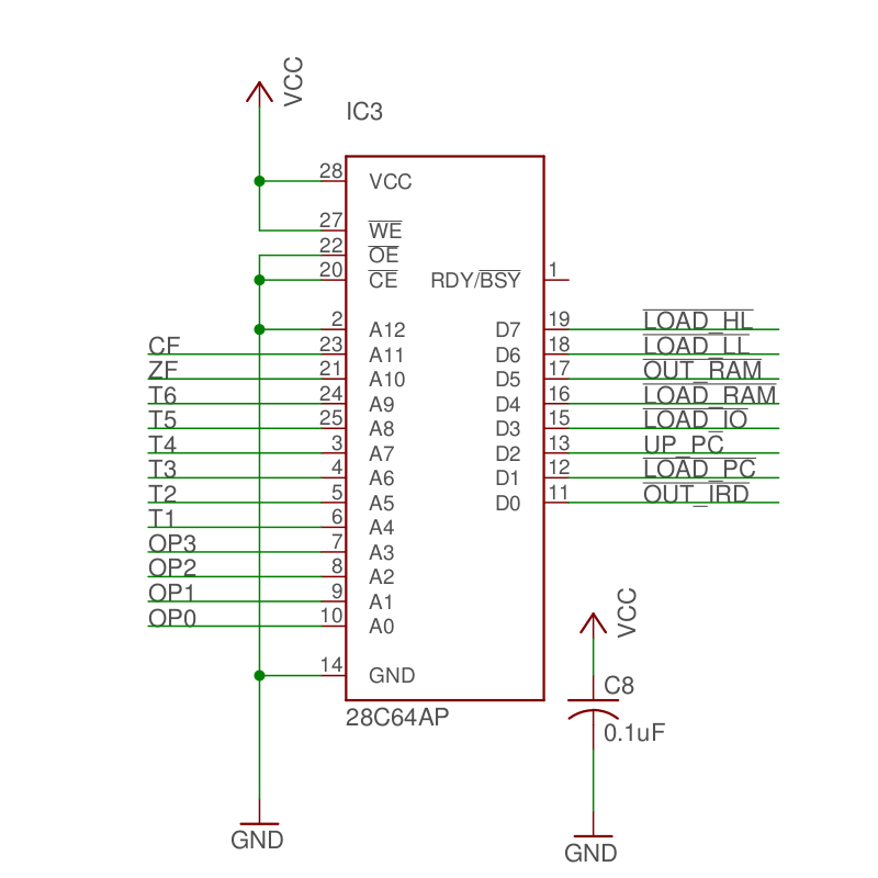
Many of you from the "software world" will know about using "lookup-tables". This is a pretty common practice when dealing with limited resource or when performance is needed. For the DDL4-CPU decoder, I am using 2 EEPROMs loaded with a lookup table. The original design had a total of 12 inputs, which includes the 4-bit opcode, 6 clock phases along with the Carry-Flag (CF) and Zero-Flag(CF). The CF and ZF inputs were present to handle conditional jumps such as "Jump on Carry" and "Jump when Zero", no other instructions make use of the Carry or Zero Flags. The problem with this implementation is that it increases the lookup-table by a factor of 4. Each input combination needs to be represented in the lookup table even if it doesn't use CF or ZF. An example of this is the command to load immediate data from the ROM to register A (LDA). Four entries in the lookup-table would have to be made. This is some pseudo code that represents the LDA command:
if [LDA==1] ; then
  if [CF==0 & ZF==0] ; then
        copy data to registerA
    else if [CF==0 & ZF==1] ; then
        copy data to registerA
    else if [CF==1 & ZF==0] ; then
        copy data to registerA
    else if [CF==1 & ZF==1] ; then
     copy data to registerA
    endif
endif
In this case, there are 4 entries that do exactly the same, no matter what the value of CF and ZF are. Not only does this increase the size of EEPROM needed, but it makes generating the lookup-table a lot more complicated. So, the question then becomes, how to solve this problem and reduce the size and complexity of the lookup-table? Well the obvious answer is to remove the CF and ZF inputs to the lookup-table and deal with the CF and ZF in another way.... to be continued!

Well, well, well.... after all the testing and planning, the first revision of the DDL4-CPU assembly is complete and ready for further testing! During the assembly and testing, I've already identified more than a dozen places for improvement, fixes and optimizations! The most notable of these is how the conditional jump with Carry Flag, and Zero Flag will be implemented (more on that soon!). However for now, there is a lot of testing that needs to be done before the next set of boards get ordered!
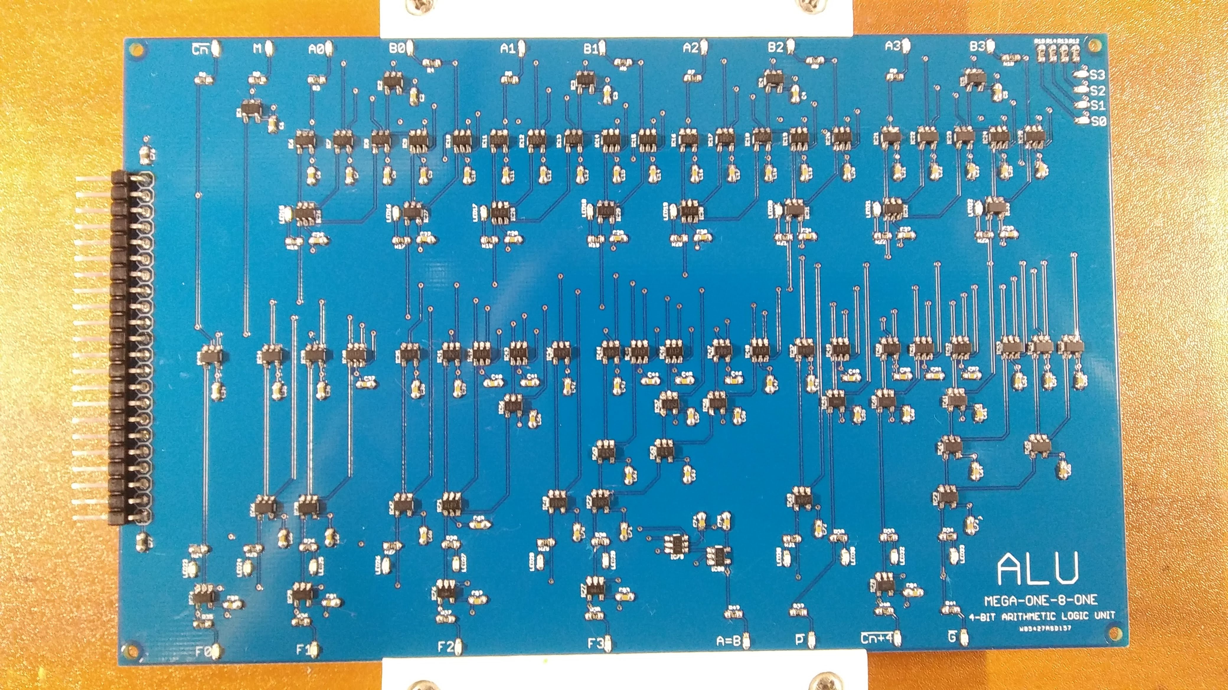
Well, at 244 components, the Mega-One-8-One, is a mega PITA to assemble by hand, but it's done none the less. The Mega-One-8-One is a gate level replica of the 74181 Arithmetic Logic Unit (ALU), which was previously highlighted on hackaday.com ( Huge 74181 is a classic ALU you can actually understand!). Since the 74181 is not available new any more (yes you can get New Old Stock or NOS), I decided to build a replica for use in the DDL4-CPU so that the math and logic functions could be more easily understood. I originally had pins on the pcb near each input and output LED, but this didn't really lend itself to interfacing into a project, so I made a second revision of the design which included a 1x22 0.1" header that allows for the quick interface to the rest of the DDL4-CPU design...
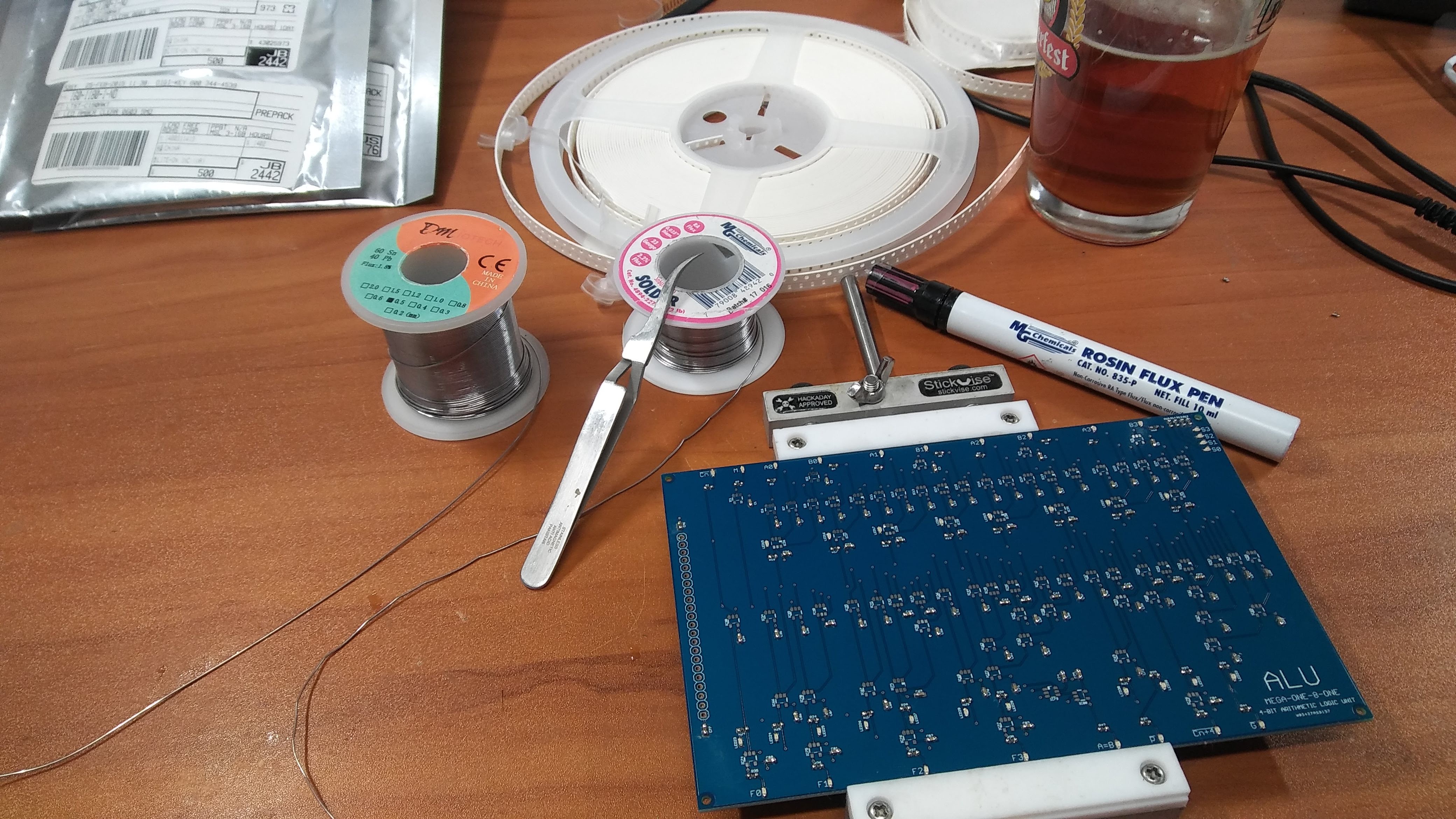
Well, after a seriously hard week of debugging some new hardware at $DAYJOB, I was able to crack open a beer, and start assembling the Mega-One-8-One for the DDL4-CPU! I've populated all the capacitors, the current limiting resistors for the LEDs, and the LEDS. To make everything fit, I used 0603 resistors, caps and LEDs for the Mega-One-8-One. The caps and resistors aren't too much of an issue as they are not polarity/orientation sensitive, but the LEDs need to place with the correct Anode/Cathode alignment. I usually can do 0603 LEDs without an issue, as the bottom of the LED has some markers to indicate orientation for the Cathode. After placement, I use my multimeter on the diode setting to step through all the LEDs to make sure they are all placed with the correct orientation.... ugh this board has a LOT of components!
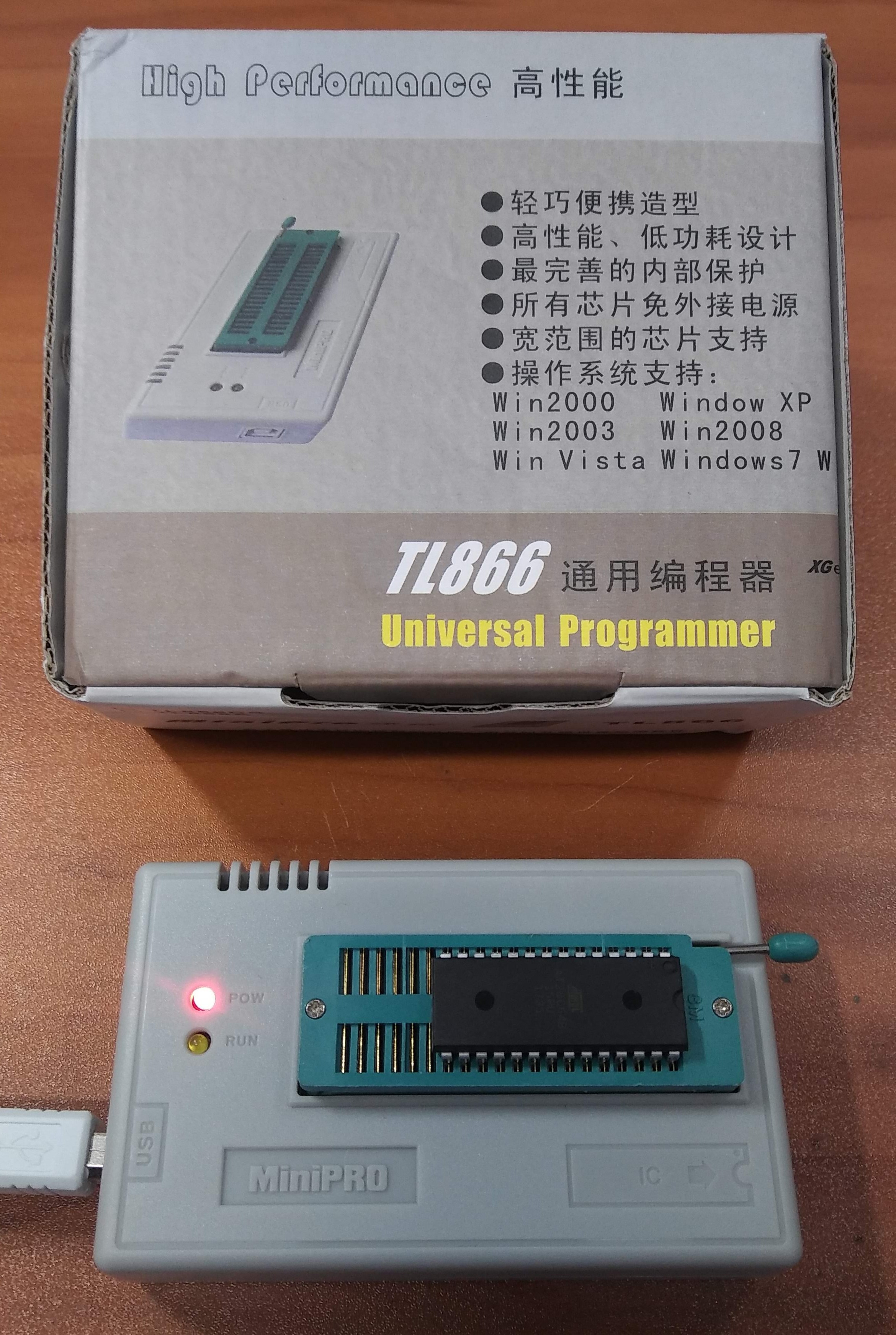
It has been over a decade since the last time I needed to program a parallel (E)EPROM of any type. Back in those days there was a parallel port on virtually every laptop and desktop computer. I ended up selling my old parallel port programmer years ago on ebay. With the build of the DDL4-CPU, it was time for me to look for something a little more modern. A quick search turned up the TL866 usb based programmer. Further searching revealed that there was a linux command line tool created for these programmers. So I ordered one! Well, I didn't read carefully enough.... there are three variations of the TL866 available, two are compatible, the third is not! The TL866 II+, is a slightly newer version that supports a wider range of voltages and has more In-System-Programming (ISP) support. So this was the one I selected to start with. The device works fine with the provided windows software, but no support available in the linux software for the TL866 II+. I ordered a second unit, this time the TL866CS (the TL866A would have worked as well). After downloading a copy of the linux tool, I was able to read and write to the EEPROM that I had selected. The linux tool did warn that the firmware on my device was old and I needed to update it. Unfortunately, the linux tool doesn't offer the capability of doing the firmware update (or none that I could find), so I ended up digging out an old windows laptop that keep around for just such occasions (I purchased it at a pawn shop for $99 - the wifi doesn't work!). After downloading the software and installing it, I flashed the new firmware, and went back to my linux setup with no more warnings! Sweet little setup!
UPDATE: someone shared the link to a linux based firmware updater!
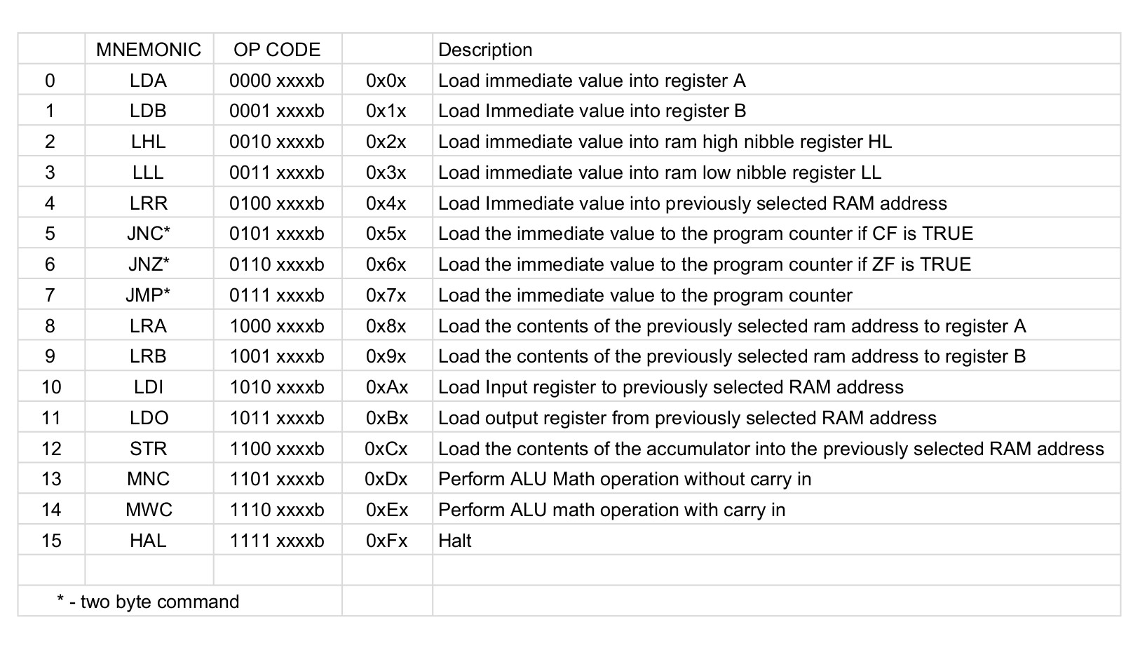
Before I began the layout of the DDL4-CPU, I came up with an initial Instruction Set Architecture (ISA) for the design. It went through several revisions as I was designing the boards and refined the components. Here at the last minute as I am programming the EEPROMs, I decided to make a few last minute changes. I am using a 4-bit opcode with a 4-bit immediate. I've also allowed for in the design to have 2-byte commands. I only plan to implement the 2-byte commands with the conditional jump commands with this revision. This is mainly to work out the details of how it should work. It was a challenge to come up with an optimal configuration. I reviewed a lot of third party designs including the TD4 cpu described in the Japanese language book "How to Build a CPU" by Iku Watanabe. A good English description of the book and contents can be found at the "Building a 4-Bit CPU" web page. You can also find a number of attempts at building a TD4 cpu on hackaday.io pages!
Create an account to leave a comment. Already have an account? Log In.
i have concidered doing the some of the AMD 2900 series bit slice stuff, i am just not sure how much interest is out there... i've gotten very little engagement on the previous designs...
Hey! That perfect!
Did you create some internal standards for board pinouts?
The pinout is not fixed on each one per se, but does have some organization to it:
1 - VCC
2-9 D[8:0]
10-19 Control signals
20 - reset
21 - master clock
22 - ground
i've added a screen shot of the RAM module interface. This is a typical interface:
https://hackaday.io/project/158510/gallery#cba33e14f4c644f1b0084ca5c6cf1a12
i left plenty of room for expansion and "white wire fixes"
Become a member to follow this project and never miss any updates
 Dave Collins
 matseng
 Amos
Amos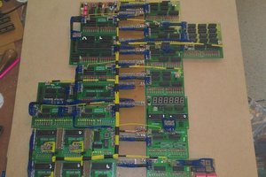
 Charlie Smith
AMD 2901 perhaps.