-
Or use a lot of diodes and a few transistors
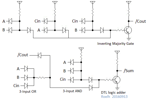
08/16/2018 at 07:23 • 2 commentsFor a more conventional ALU approach, using resistors in the base connections, the following adder circuit could be used as a starting point. It could also be used for DVTL ( Diode-Vacuum-Tube-Logic).
![]()
The top part calculates the (inverted) carry. The lower part calculates the (inverted) sum, with the function SUM = ( ( A or B or Cin ) and /Cout ) or ( A and B and Cin )
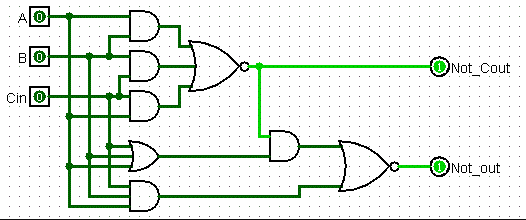
The logic equivalent of this circuit is:
![]()
With a few extra parts, the carry could be forced to always be active or inactive. In that case the circuit will perform a simple AND (for carry active, /Cout=low) or an OR (for carry not active, /Cout=high).
To connect the /Cout to Cin of the following bit, you will need an extra transistor inverter, or you could use inverted logic for every alternate bit.
To make this into a working ALU, resistor values must be calculated and some parts must be added for optimal circuit response. It is supposed that the circuits connected to the inputs can sink current but also source current (for the OR gate).
It is a simple circuit. It does not have a fast carry.
[ edit oct 2023: pictures were deleted by Hackaday, I re-inserted them ]
-
Full ALU design
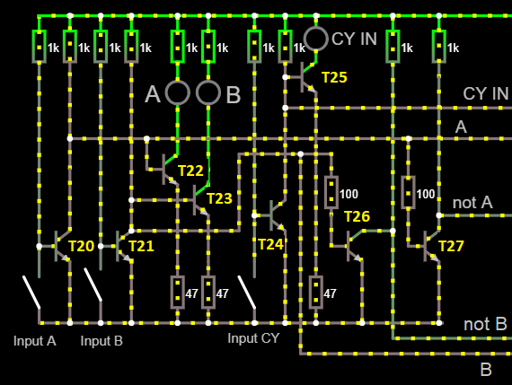
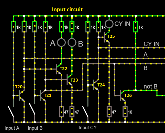
08/04/2018 at 21:02 • 2 commentsThe full ALU design also has two parts in the schematic, the first part creates the input signals again, main difference is that now also the A signal is available in complement form:
![]()
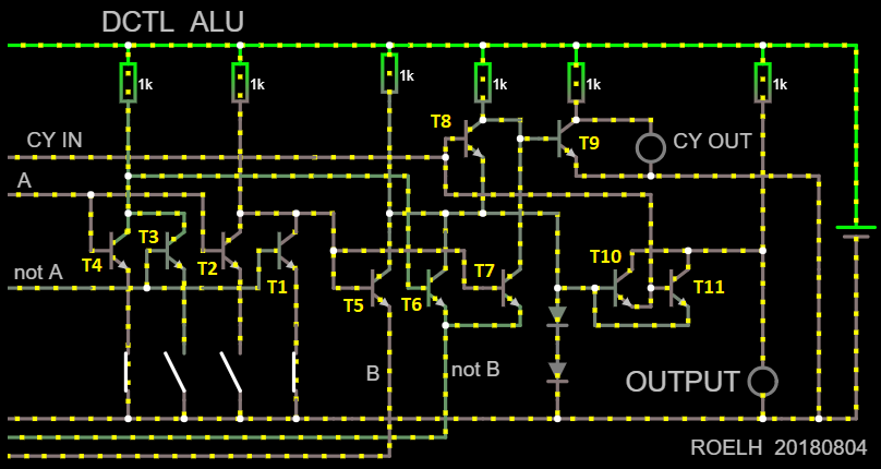
And the following part is the actual ALU. The ALU needs both straight and inverted inputs for A and B. Since these are probably already available (because the flipflops in the CPU will have both outputs), the inverters of these signals are not included in the transistor count of the ALU.
![]()
At the lower left side, you see four switches that control the function of the ALU. The switch positions for the main functions are:
![]()
In reality, the switches should be replaced by transistors. These transistors can be in common for several bits (4 bits or perhaps even 8).
One thing must still be added to the ALU, that is a transistor that forces the input carry to zero for the logical functions. That makes it a 12-transistor design. So in this simulation, the CY-IN must be set to zero for the logic functions.
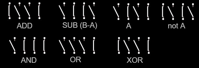
Although only seven functions are shown for the switches, the four signals can select every theoretical possible function of two binary inputs. This includes inverted versions of AND, OR and XOR, and the input B and inverted B.
The simulation can be quite surprising. Did you know that a bipolar transistor can also work backwards (current flowing between emitter and collector in opposite direction) ? This actually occurs in a certain input arrangement, but it did not have an effect on the logic output.
Not mentioned yet.... supply is 5 volts. The transistors are general NPN transistors that are available in the simulator.
This is a ripple carry adder. The carry signal has to pass T8 and T9. If this is not fast enough, I would at first check the influence of the circuit that is connected to the emitter of T8. The carry could also be made two times faster by calculating it for two bits at a time.
-
Full adder
08/04/2018 at 20:22 • 0 commentsThe Falstad simulation of the full adder has two parts. The first part creates the input signals for the adder:
![]()
There are switches to change the input signals A and B, and the Carry input signal. There are also 3 LED's to check the input values. At the right side you see the 3 created signals CY-IN, A and B, and an inverted version from B.
The second part is the actual adder:
![]()
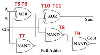
This is actually an implementation of a classic adder design. The following picture shows the function of the transistors:
![]()
ALU in DCTL technology
A full ALU, capable of ADD, SUB and all logic functions, with only 12 transistors