Pavel
Pavel-
State Machine and instruction types
12/30/2021 at 18:03 • 0 commentsWhen I was coming up with new Register Transfer Scheme, and in general while rethinking the design approach for this CPU, I realised that the explicit state machine will be the way to go. At the time I thought it would consist of quite a few of states. But while devising the ways words need to be shuffled around the CPU (to enumerate needed states) for every instruction, I found out that there is a lot of commonalities between some of the states, and they can be grouped so that difference between them would be one or two signal lines. It occurred to me that there is a way to make the number of states low, but have the variations inside states that would be disambiguated via combinatorial circuits. Example would be Load/Store state, they have a common pattern for addressing logic, but different for the data moving logic. Yet, this difference can be wholly controlled by just one bit in instruction, which makes trivial the disambiguation.
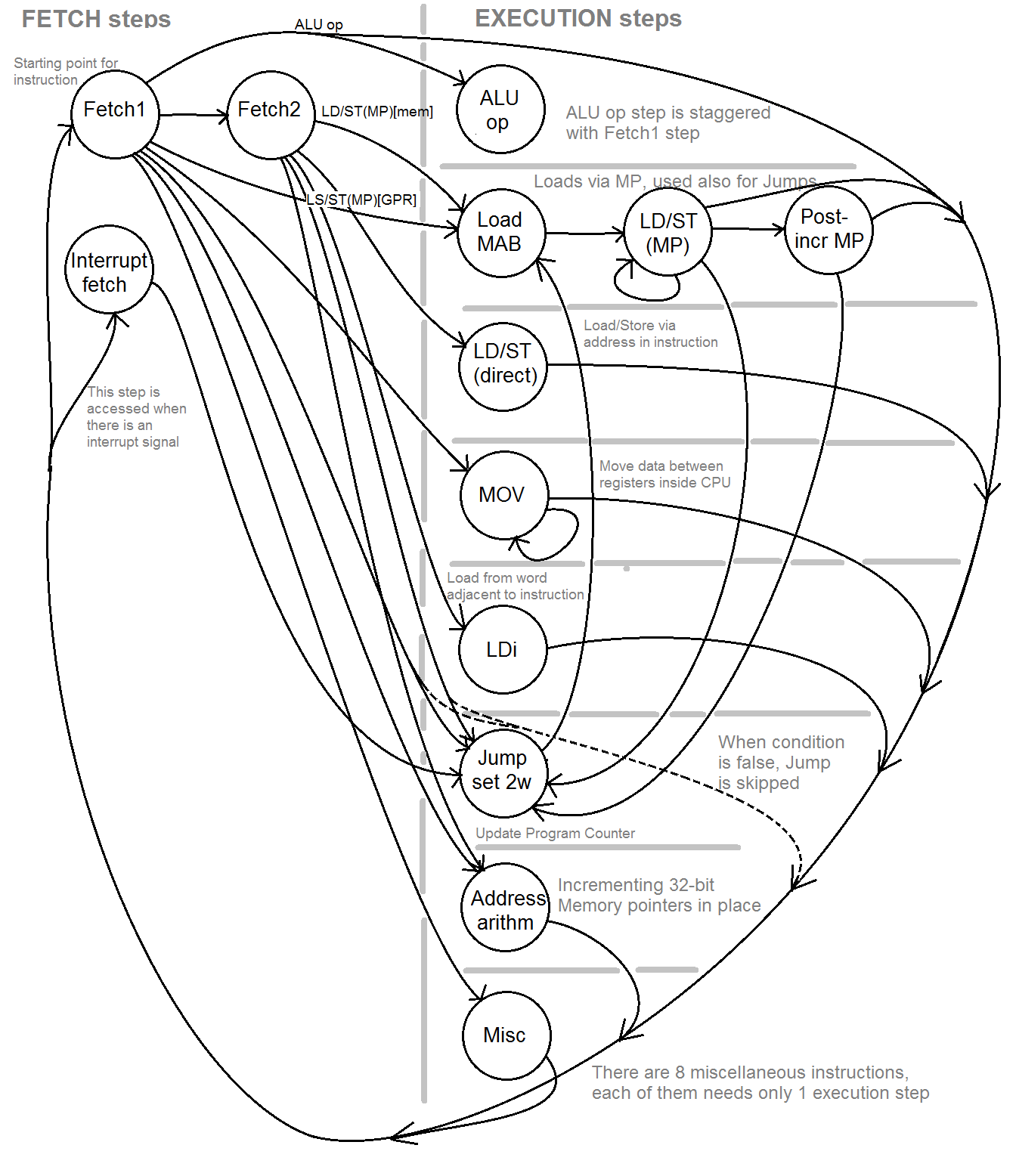
Thus I weeded the total number of states to 3 fetch states and 10 execution states.Here is a diagram which shows these states and transitions between them:
![]()
As can be visible from the diagram, there are 8 instruction types:
1: ALU operations -- all are executed in 1 step and decoded inside Calculating Core; the next instruction is fetched in parallel
2: Loads/Stores via MP +offset -- set of 8 instruction pairs (load/Store) of variable length of execution
3: Loads/Stores via direct address
4: MOV -- copying of data between registers
5: LDi -- loading immediate value into register
6: Jumps -- set of 8 conditional and 2 unconditional instructions updating Program Counter, use the same states as (2)
7: Address Arithmetic -- arithmetic operations on 32-bit values in MP (adding 8- and 16-bit signed values to MP)
8: miscellaneous -- different instructions like NOP, HLT, SetIM, multi-word prefix etc.
These instructions comprise the full set intended for my CPU.
-
Dealing with Jumps and Interrupts
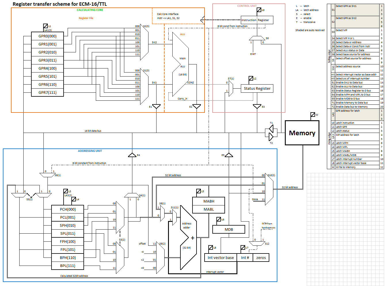
12/29/2021 at 15:40 • 0 commentsDuring more rigorous contemplation of interrupt mechanisms, I found out that there needs some adjustments to be done to the Register Transfer Scheme.
Here is the updated one:
![]()
The new things added are 32-bit Interrupt Vector register, and a couple of associated selectors.
I think I finally got it about how to implement interrupts. It was quite perplexing, and I thought it should have to be some complex sequence, and I also regarded it as not a pressing issue and haven't given them much thought. Now, really thinking about interrupts, I came up with seemingly good solution -- just use the sequence for Jump to Subroutine, just with some tweaks. Below is more in-depth discussion:
First, the Jump sequences:
Regular Jumps are 2-word loads to PC via MP (+ offset).
Jump instruction sequence
0 Fetch1 // load IR <-- Mem:PC; PC <-- PC+2
0' (Fetch2) // load MDB <-- Mem:PC; PC <-- PC+2
1 Set 2w flag
2 Load MAB <-- MP+offset // offset may be GPR or MDB
3 Load PCH <-- Mem:MAB; load MAB <-- MAB+2
3* Load PCL <-- Mem:MAB; load MAB <-- MAB+2The regular Jumps are Unconditional Jump, and 8 jumps on different conditions:
jump on Carry, Overflow, Negative, Zero, Not Carry, Not Overflow, Not Negative, and Not Zero.
The Jump to Subroutine is in Jump family, but it has additional steps in sequence:
it is a 2-word store of PC via MP -4 (stack pointer), followed by 2-word load to PC via PC+offset.
Offset source, code and Stack pointer are the same as corresponding parts of regular memory transfer via MP instructions
JSR instr sequence
0 Fetch1 // load IR <-- Mem:PC; PC <-- PC+2
0' (Fetch2) // load MDB <-- Mem:PC; PC <-- PC+2
1 Set 2w flag
2 Load MAB <-- MP-4 // most common MP will be SP
3 Store Mem:MAB <-- PCH; MAB <-- MAB+2
3* Store Mem:MAB <-- PCL; MAB <-- MAB+2
4 Set 2w flag
5 Load MAB <-- PC+offset // offset may be GPR or MDB
6 Load PCH <-- Mem:MAB; MAB <-- MAB+2
6* Load PCL <-- Mem:MAB; MAB <-- MAB+2In this way the jump (Program Counter load) is preceded by storing the PC value to current stack tip, thus making it possible to return from the subroutine by loading stored PC value from Stack to PC.
Enter Interrupt -- this instruction I thought would be something very special, and quite complex, but, as it looks like right now, turned out not that difficult. It was possible to implement it with special Fetch cycle, which updates the Instruction Register with hardcoded value of one type of JSR, without PC update, and a signal which substitutes address from Memory Pointer with address from Interrupt Vector register.
It can be triggered explicitly, in code (software interrupt), or via hardware. In the last case the interrupt sequence is followed after the last step of currently executing instruction.The hardcoded JSR used for entering interrupt uses SP_h/SP_l pair of Memory Pointer registers forming the Stack Pointer. In this way, this single instruction enforces the convention of using this memory pointer as the default Stack Pointer.
-
Memory Pointers description
12/24/2021 at 21:05 • 0 commentsThere are 8 16-bit registers paired to yield 4 effective 32-bit Memory Pointer Registers. Each of these 8 registers can be accessed and written to independently. But they are used in pairs as source of memory address. In some cases they provide direct address, while in others, these memory pointers contain a base for address, while the address itself is calculated as this base plus some offset value, which can be provided from one of the General Purpose Registers, or from immediate value in memory right after the instruction word.
Of these Memory Pointers, the first one, the Program Counter (PC) is special in a sense that it is implicitly used for fetch cycle at start of every instruction execution sequence as the source of address of that instruction, and has its value updated each time. It also is the implicit register for loading new instruction address in Jump instructions. Otherwise it can be accessed the same way as all three other MP registers.
For these other 3 Memory Pointers, the distinction between Stack Pointer (SP), Frame Pointer (FP) and Base Pointer (BP) is only conventional, and they are really fully interchangeable.
In the instruction set I am developing, there is no dedicated operations related to stack -- all the needed memory transfers for creating a stack structure are already present in a set of Load/Store operations.
The list of main instructions/instruction types is presented in separate log entry together with state machine description.
The in-depth instruction descriptions are presented in separate project.
-
Contemplation of multi-word data transfers inside ECM-16/TTL computer
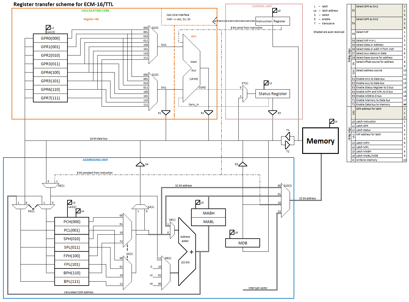
12/23/2021 at 19:16 • 2 commentsThis is an expansion over addressing logic structure described previously.
I think there is a need for providing a means to transfer blocks of data between registers and between registers and memory in a single instruction. This should increase execution speeds, especially where data-intensive calculations take place, tight cycles over arrays, and frequent procedure calls, where much of the data needs to be transferred from registers to stack and back. It also will somewhat decrease program size.
Execution speedup will be achieved with faster memory access operations: as the memory access operation takes several cycles to execute, mainly due to steps leading to address calculation, transferring several additional words will lengthen the operation execution by the number of cycles equal to the size of block in words. For example, if one-word transfer takes 4 cycles to execute, then two-word transfer will only take 5 cycles (instead of 8 cycles for 2 one-word transfers). Only penalty is 1-cycle prefix instruction for setting flag for number of words in transfer.
Overall, execution cycles could be saved when using these multi-word data transfers. There are several types of memory access instructions depending on the address source, and they can take different number of cycles to execute in default mode (1-word accesses, can take 3, 4 or 5 cycles). But even in the least favourable case, when the access is relatively fast (only 3 cycles), and the need is only for 2 consecutive words at a time, this kind of multi-word transfer still makes sense as it saves 1 cycle (5 cycles for prefixed instruction vs 6 cycles for 2 consecutive 3-cycle instructions). For all other cases, savings rapidly increase with block length, and with instructions that intrinsically take more time to execute.
As for the program size, prefix will add 1 word, so for 1-word memory access instructions, there will be no difference, code size wise, as to have single double-word access, or two single-word access instructions. For two-word instructions, and for block sizes of 4 words or more, the code size savings become apparent.
Technicalities
![]()
How to implement such transfers?
In the Memory Address Unit, the output from MAB register is to be routed back to Address Adder via 2-to-1 mux (S8 on scheme above). By default (mux control: 0), Memory Pointer is provided to "Base" input of the adder. When multi-word transfer is executed, after transferring the first word, the mux control becomes 1, and MAB now is "Base" input, while "offset" is set to "+2".
In the Control Unit there should be presettable counter which is set directly by prefix instruction. There also should be additional circuitry for overriding/modifying register address in instruction so as to transfer each word in the block to/from different register. For simplicity, some restrictions could be imposed: the lower bits of register address will need to be set to zero (or be ignored), so the instructions for double-word transfers could only have even reg addresses, ones for four-word transfers will address reg 0 and 4, and so on. Otherwise an additional small adder will be needed, and it will introduce some additional delay.
The prefix would be a one-off, meaning any flags set by it will be cleared after execution of prefixed instruction. It would need to be inserted before each transfer instruction to make it multi-word, and also there will be no need for special clearing instruction afterwards, if single-word transfer is needed. Thus these flags are not to be saved, and will not appear inside Status register.
Flags:
"2" -- transfer of two words to/from a pair of registers
"4" -- transfer of four words to/from a half of Register File or half of MemPointer File
"8" -- transfer of eight words to/from whole Register File or MemPointer File
"16" -- transfer of 16 words to/from all registers at onceThe instruction loading all the registers at once will have an effect of almost total context switch, as all memory pointers together with all GPR will receive new data, so, the PC, SP, FP and BP will have new values, and execution can start from other part of memory, and stack-related pointers will point to other stack. It can be used as return from call.
Regarding transfers of single byte: this can be done with some modification of memory system, and will introduce some delay, but not that much. These will be like single-word transfers, but will take one cycle longer. For byte transfer, 8 least significant bytes will be used. I am still in doubt if this is really needed. It will consume 1 bit of address offset, making the maximum offset half as big -- it will be +-32767 bytes instead of +-32767 words. How significant is this? May turn out not significant at all, as most offsets to be used are much closer.
-
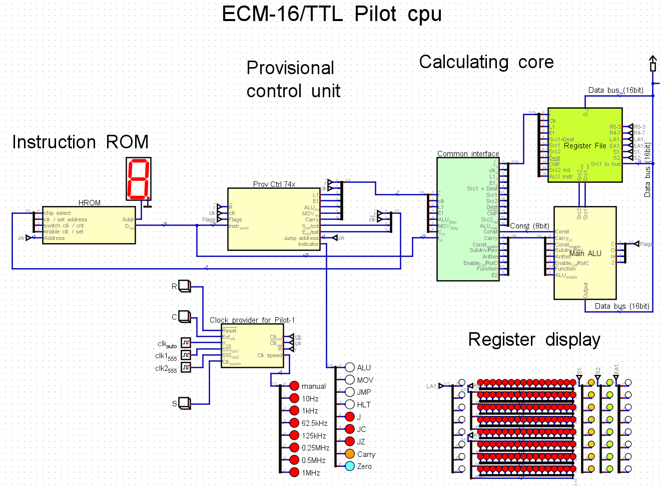
ECM-16/TTL Pilot-1 computer
11/16/2021 at 09:06 • 0 commentsUPD: I created a new project dedicated exclusively for this Pilot-1 cpu.
This is fully functional, albeit severely limited, automated calculating machine.
It can be viewed as having a kind of Harvard architecture, as it has all instructions in ROM, and data is in RAM (registers actually).
The limitations are -- the program can be max 16 instructions long, and there are only 8 registers where data can be operated on.
As all the registers' data are visible on register display, it presents a good view in process of calculation -- all those lights blinking!
This machine features full Main ALU together with Register File, completing the Calculating Core, with slapped-on Provisional Control Unit and HROM, that makes it whole.
It is a good milestone towards full-fledged computer, that supposed to have full addressing and control circuitry, as well as proper memory and I/O. As it is now, it gives some taste of what it will become some day.
Here is block diagram of this contraption:
![]()
And here is what it looked like when I first assembled it fully and tried to run it:
There are several issues, mostly due to some unexpected behaviour of HROM board, and probably there are some bugs in the control board causing intermittent resets.
The HROM had been lying around for a year, and it seems like it sustained some damage causing intermittent shorts on data line B. The glitches on the control board also haven't gone away.
I hope, in the near future I'll weed out all these bugs, and system will work fully as intended. After this, next phase will be building memory access adder and registers, and combining them into single unit. In parallel, there will be finalisation of the instruction set and design of control logic.
-
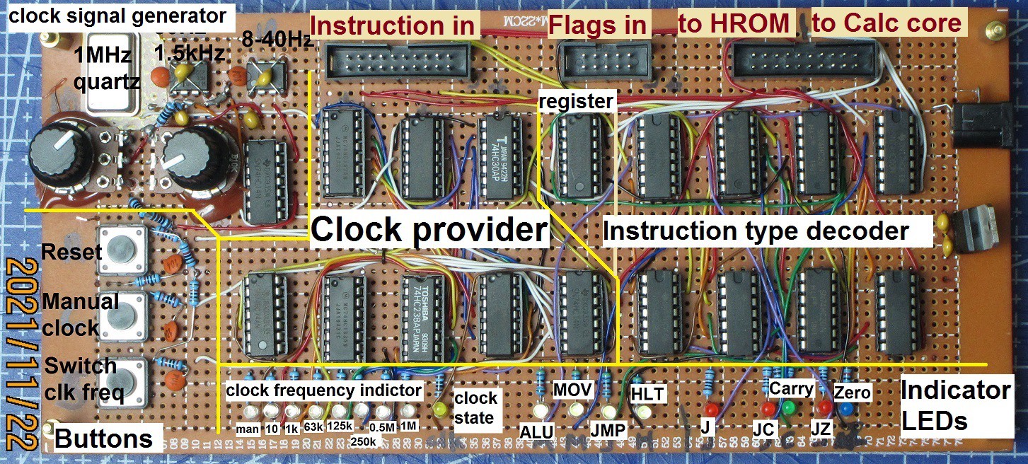
Provisional Control Unit
11/08/2021 at 09:46 • 0 commentsThis is a board that is providing sequencing for the Pilot-1 calculating machine:
![]()
It may be divided into several function blocks:
Instruction type decoder:
It is recognizing 4 types of instructions: ALU, MOV, JMP and HLT:
ALU instructions are for dealing with data modification in registers.
MOV instructions are for moving data between registers.
JMP instructions load address into 74hc163 counter inside the HROM board, thus effectively moving instruction pointer anywhere inside this 16-word instruction ROM; there are 3 kinds of these: unconditional jump, jump on carry, and jump on zero.
HLT instruction is the one that turns off counting, and makes instruction pointer stuck on its address, making machine to be stuck looping just this instruction, halting any further execution. Can only be undone via Reset.
Register:
Carry and Zero flags are saved in 74hc74 dual D-flip-flop chip, to serve as Carry_in for ALU ops, and as flags for conditional jumps.
Clock pulse generation:
Multiple clock frequencies are provided: 1 manual, and 7 auto ( from roughly 10Hz up to 1MHz, which can be seamlessly switched between ). Two slowest frequencies (~10Hz and ~100Hz) are generated using 555 chips and can be smoothly adjusted via potentiometers, while higher 5 frequencies are derived from 1 MHz crystal oscillator and its signal progressively divided by 74hc163 synchronous counter.
Buttons:
Reset, clock pulse, switch frequency.
LEDs:
Indicating:
- main instruction type, and jump subtype;
- C and Z flag value;
- current clock frequency;
- clock signal state;
- Reset signal state.
Preliminary testing results:
For now I tested board all by itself, and it appears to work mostly as expected, but there are some issues:- I cannot access 5 highest clock speeds provided by crystal oscillator, somehow it switches all the way through right away after I release "change frequency" button (on falling edge), while it supposed to do the switching only when pressed on (rising edge).
- probably related to, and most certainly causes the above problem is the presence of some spurious signals which cause the flipping of flag values in register when clock signal is at high level, and instruction is JUMP (the registers supposed to set/reset only during ALU instruction).
These issues are probably due to coupling of high frequency signals coming from crystal and counter used to divide this signal frequency.
Plans:
In a couple of days I will test this board integrated with HROM and Calculating core as the Pilot-1 machine. I hope the above issues will not be blockers for working of the integrated whole, or will not be too difficult to solve. (Maybe just disconnecting power from crystal will be workable workaround, although in this case highest clock frequency bill only be 1.5 kHz).
-
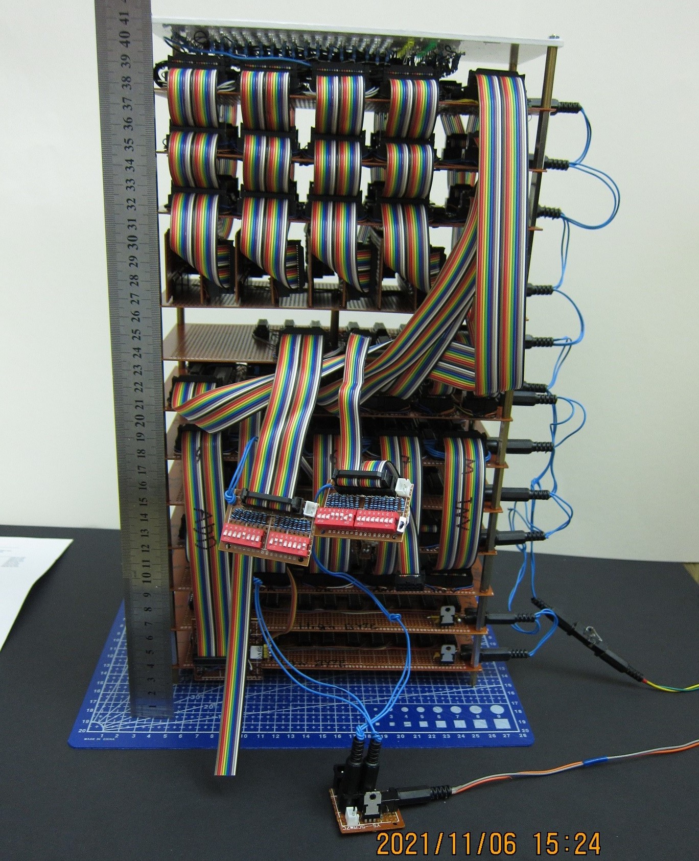
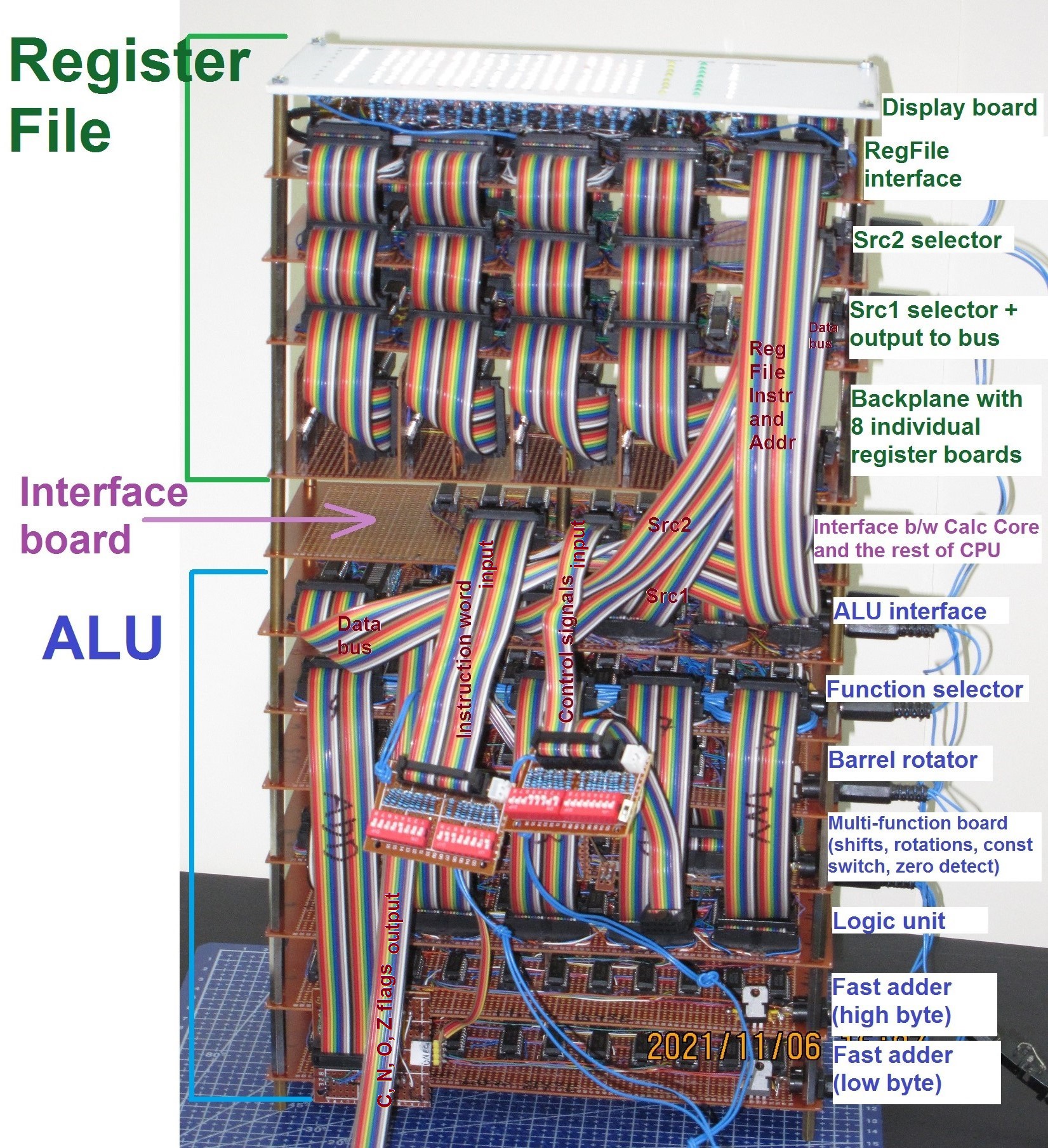
Calculating Core complete!
11/06/2021 at 15:43 • 0 commentsCurrent state of affairs:
The full stack for calculating core (ALU + Register File + Interface board) of this CPU is completed! And it is circa 40 cm high!
![]()
After completing the interface board back in August, I've stacked this whole thing for the first time. When I started testing it, something was odd -- the thing was working erratically, some instructions were working seemingly ok, some others worked erroneously, yet others weren't working at all. At the time I disassembled and assembled the stack several times, but haven't been able to weed off all the bugs, and after a while I've got interested in some other things.
Now, I've returned to this project, disassembled and took hard look at the boards comprising the Register File, took a good note of all the connectors, which signal gets to which wire, and found that in several places those wires were soldered to wrong inputs/outputs! Somehow this eluded me earlier. Anyway, after wiring bugs were sorted out, I've assembled it all, and now it seem to work ok. All the instruction types this Calculating Core is supposed to support are working ok, as far as I can tell.
Now, this is a milestone passed, and I have a device with which I can do real calculations, provided right sequence of instructions. For now, these instructions can only be entered manually, one by one via a couple of switch banks.
Plans for the next steps:
In the next few weeks I plan to make a provisional control unit, which together with the Calculating Core and HROM will make the automatic calculation machine. It will not be a full-fledged computer, but a milestone towards it. I call it Pilot-1 for the lack of better name.
Pilot-1 machine will have a 16-word ROM for its instructions, and will operate only on its 8 general purpose registers.
Supported instructions are all ALU instructions, the MOVs, and Jumps, conditional and unconditional. The latter ones are really needed to make maximum use out of only 16 instructions that can be inside the ROM.
This Pilot-1 thing will not have any conventional I/O, aside from reset button and clock switch. Luckily, instructions are entered via switches on ROM board, and results are visible on display board, this should look like impressive light show. Blinky lights, yay!
Pictures:
The Calculating Core board stack :
![]()
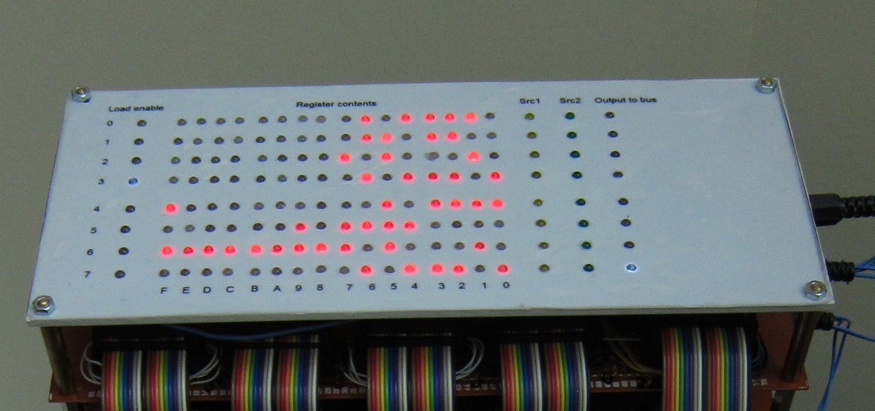
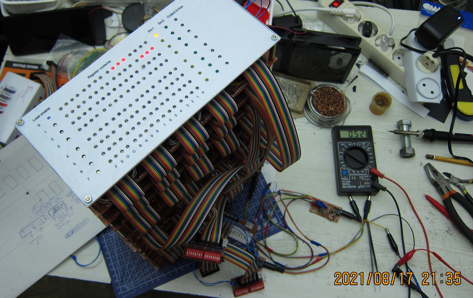
The Register Display board in action:
![]()
Current control interface:
![]()
-
Instruction translator board for ALU/RegFile
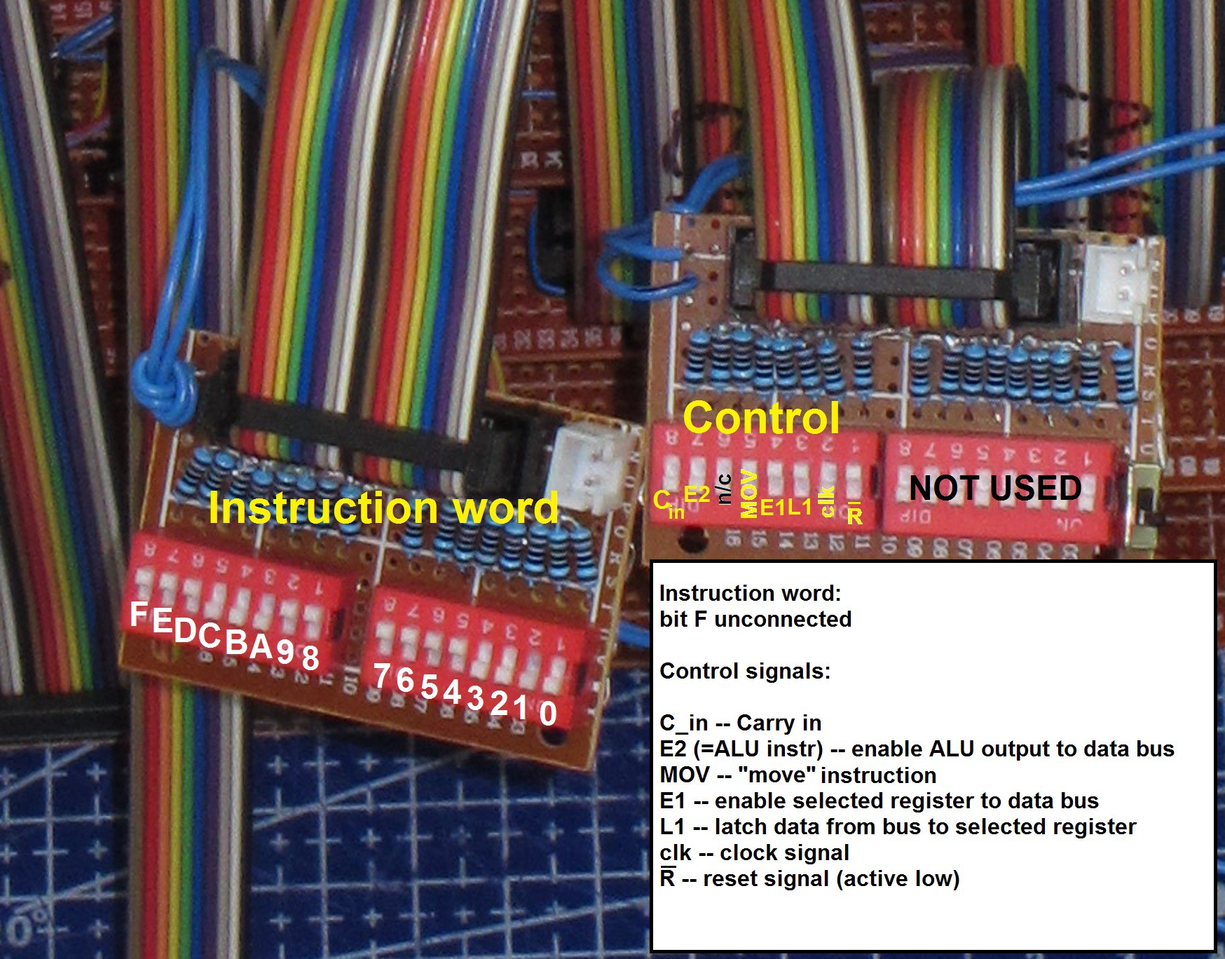
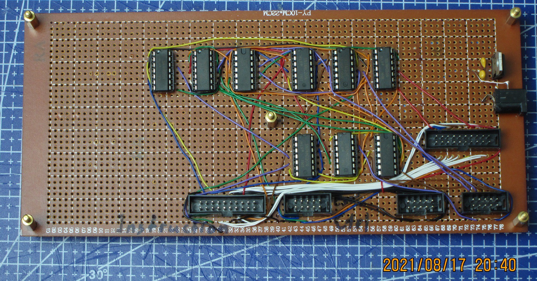
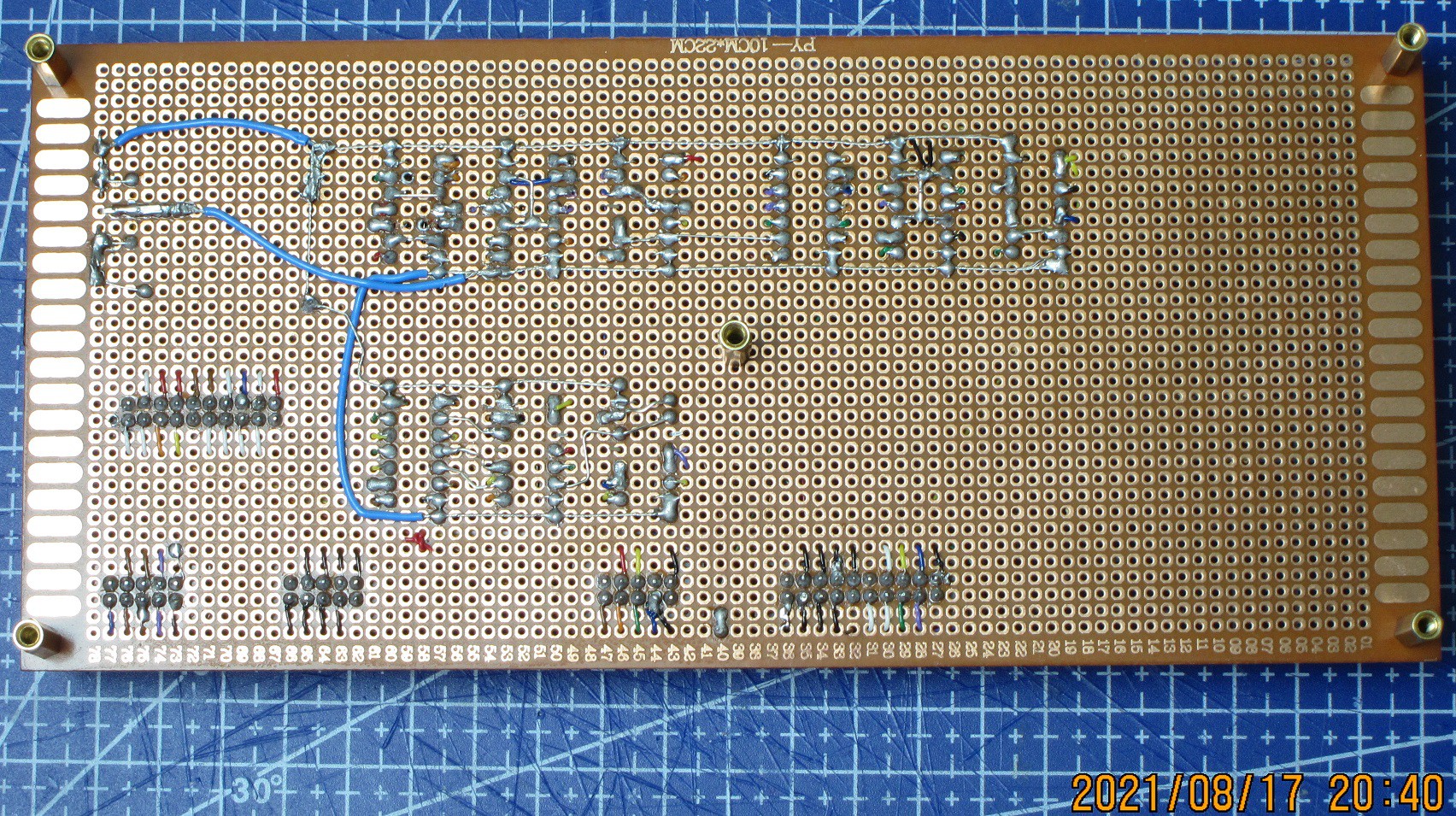
08/16/2021 at 15:38 • 0 commentsThis board with a handful of chips serves as control interface between Calculating Core (ALU/RegFile assembly) and the rest of CPU.
It mostly does decoding of ALU instructions into ALU control signals, constant value, and register addresses. It also takes in ~R, clk, and a couple of control signals from Control Unit (yet to be developed) and distributes them to Calculating Core accordingly.
Here is the board:
![]()
![]()
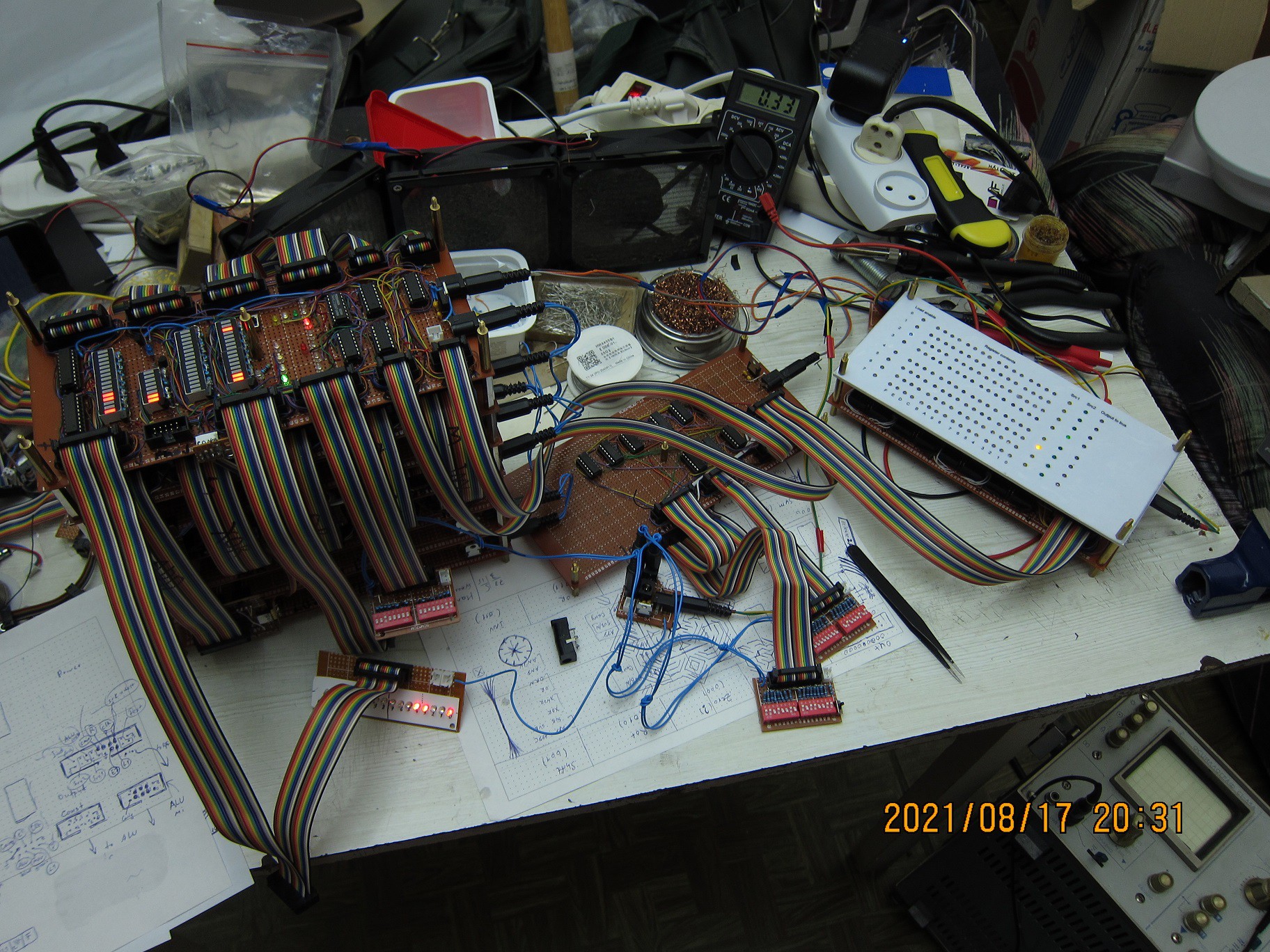
And here are a couple views of testing process for the whole calculating core:
![]()
![]()
-
Display / interface board is complete
08/06/2021 at 13:45 • 0 commentsThe registers content display, along with its control board, which also serves as control interface for the whole register file, is done.
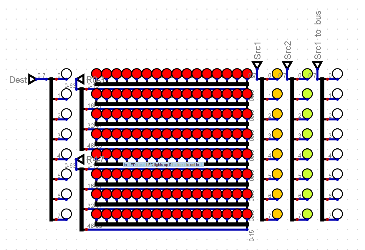
The display contains 160 LEDs, which show what is contained inside of each of 8 General Purpose Registers, along with indications of which of them is going to be loaded from bus, which is enabled to bus, and which one serves as Src1 or Src2 inputs for the main ALU.
Color arrangement of the display:
![]()
Display is made from 3mm thick white plastic, to the same dimensions as all the PCBs, so it can be stacked on top of other boards. I drilled holes in it so the LEDs are nicely fitted. Since I did it by hand, it shows in somewhat uneven spacing, but overall I am satisfied with its look.
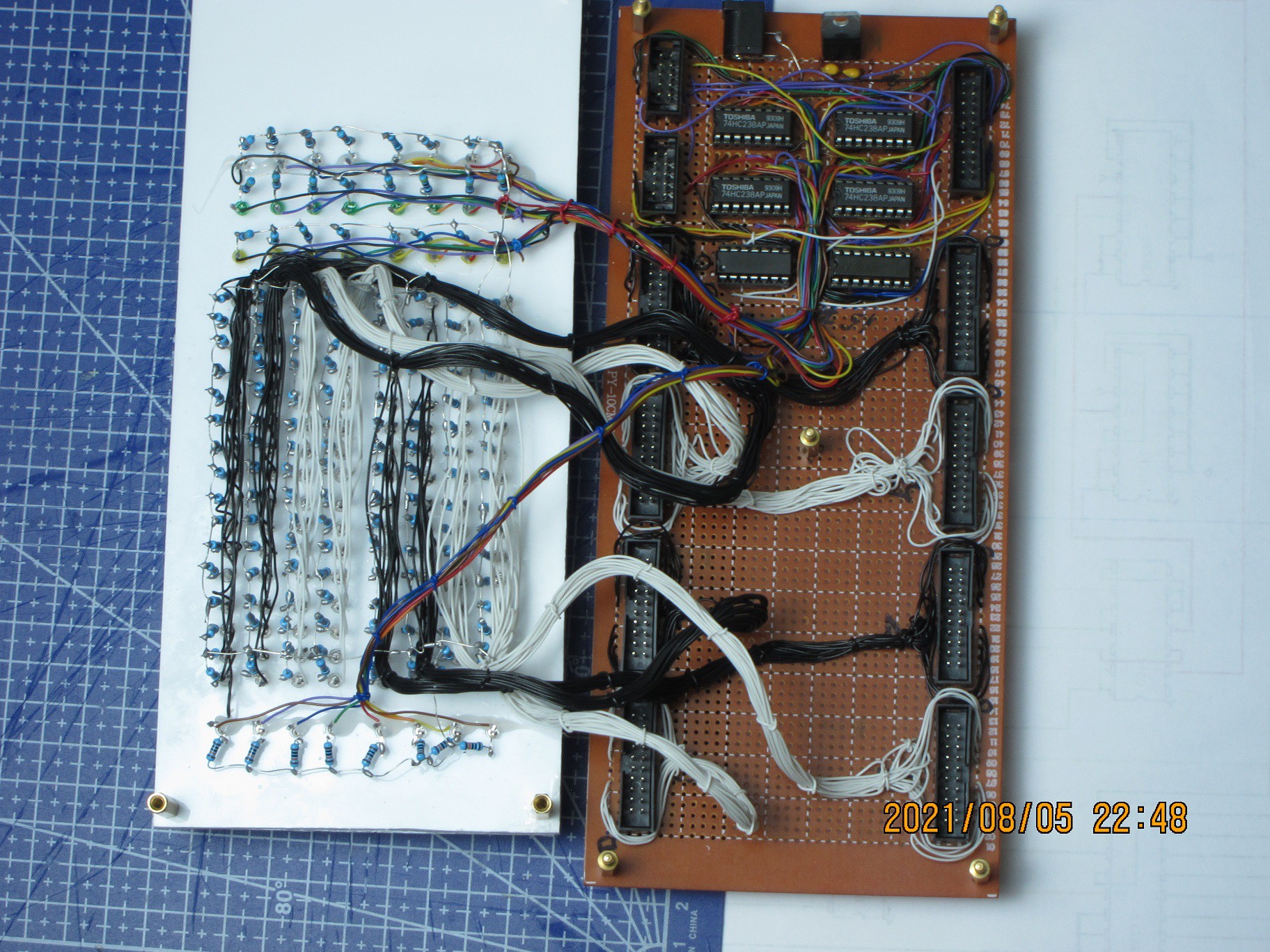
This part contains only 6 ICs, but there are a lot of connections:
![]()
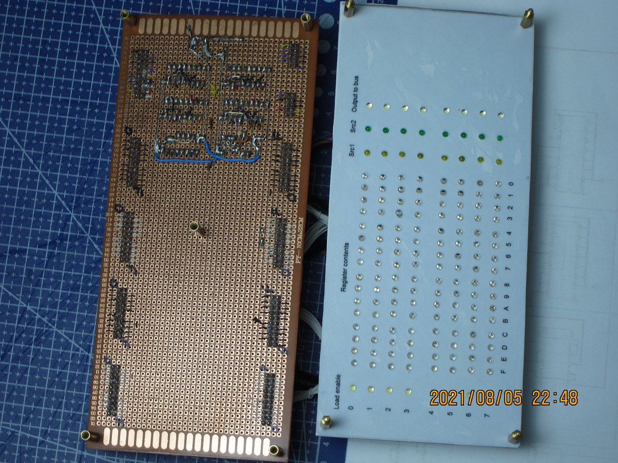
Here is the other side:
![]()
And here the whole Register File stack, as seen from the side (there are some ribbon cables missing though):
![]()
---------------------------------------------------
Next I want to make the Instruction Translation board for the ALU, and Provisional Decoder board: with these, and my 16-word ROM I will be able to integrate all the parts made to date into functional, albeit very limited, Harward-architecture type computer. It will have only 16 words for instructions, and only 8 words of volatile memory (actually, the Register File, just completed).
This computer would be called "ECM-16/TTL Pilot", as this will be the first integrated test of the system, which will be capable to perform automated sequence of operations.
Next, the addressing circuitry, which will be almost as complex as the whole Pilot, with proper Instruction Decode, Memory, Storage and Interface parts will be built, so the proper computer system is to be achieved.
-
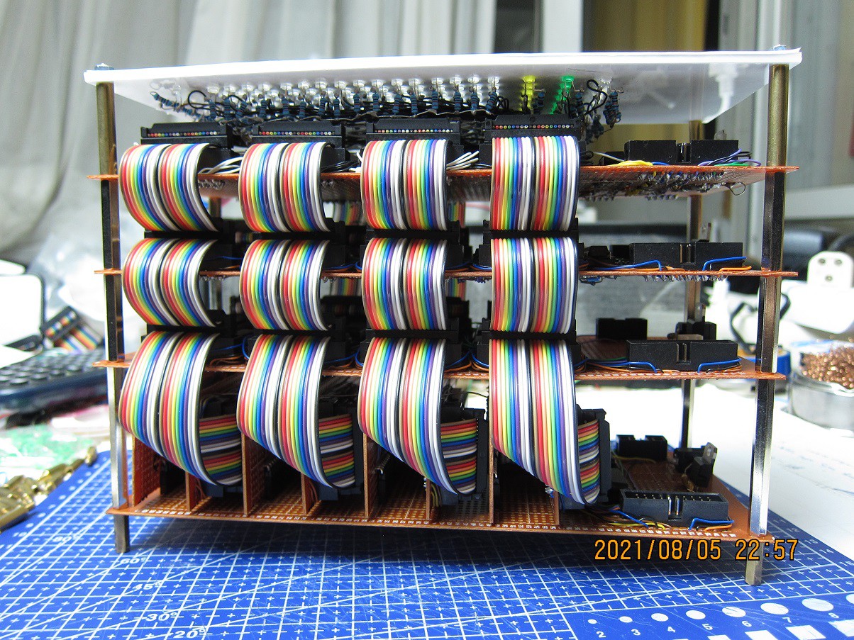
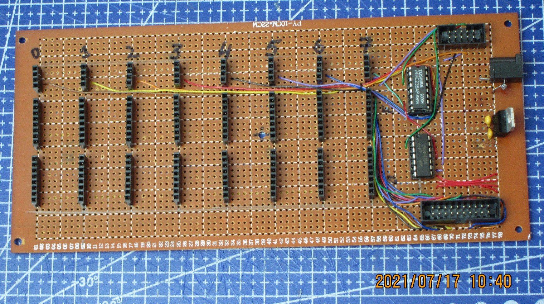
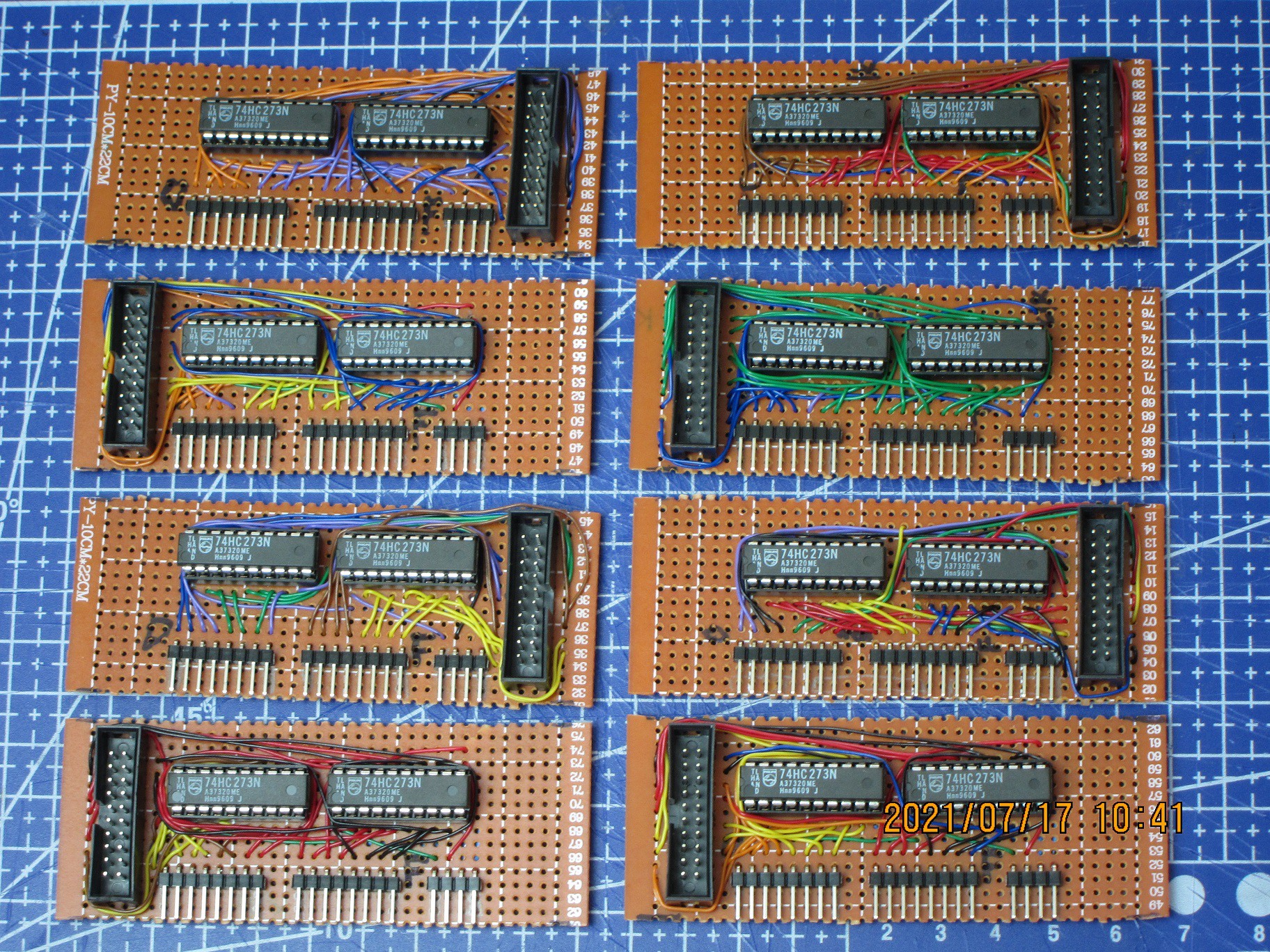
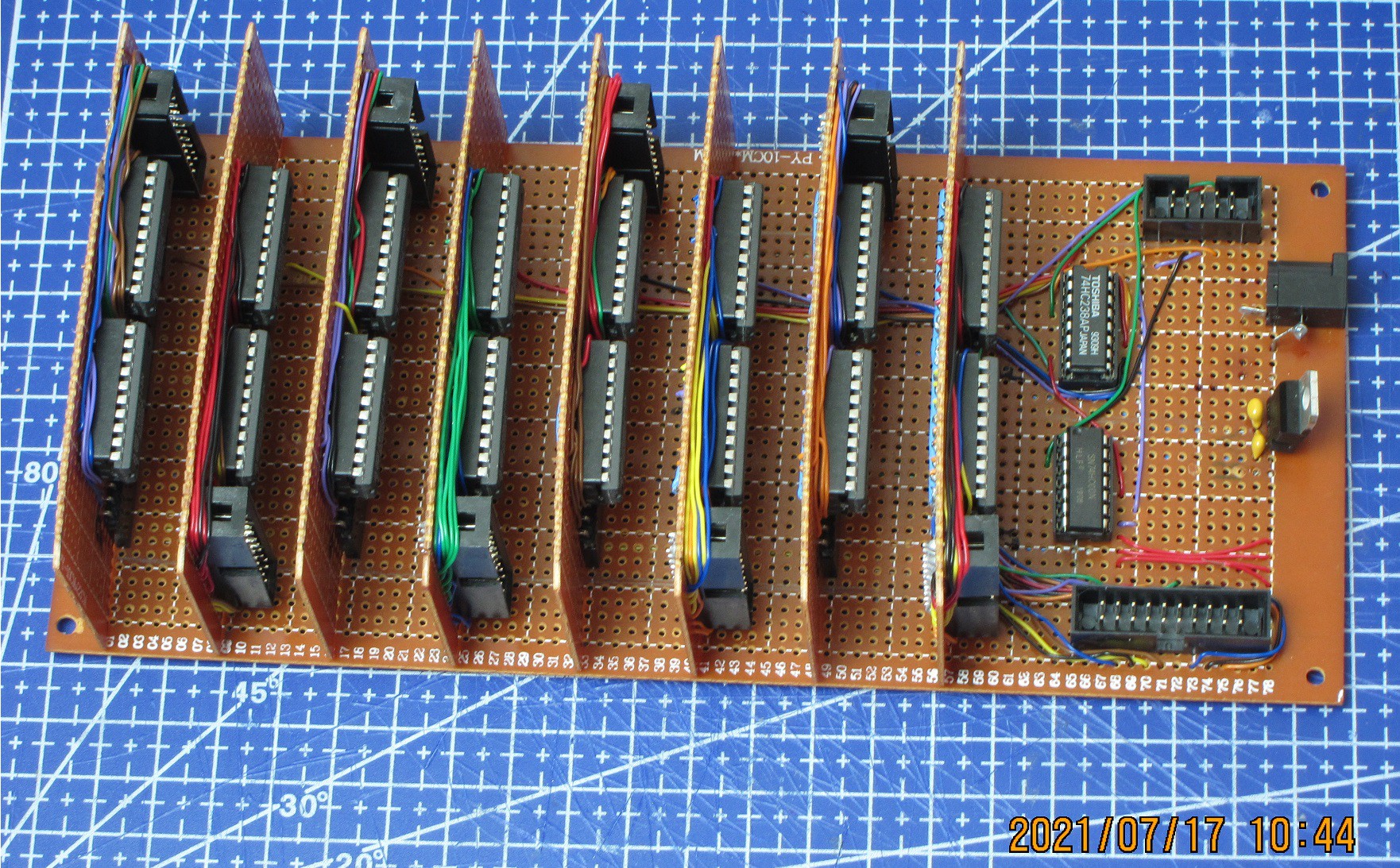
Backplane and register boards are complete
07/17/2021 at 17:09 • 0 commentsThe "Backplane" board along with 8 register mini-boards are completed.
This is the main part of Register File, where data is being held.
Each mini-board contains a 16-bit register and output IDC connector, as well as a row of pin header connectors through which they connect with backplane board. The backplane itself provides data input, and selection of register to be written, as well as power.
Next part will be LED display of data in registers. It will consist of two boards - one with all the wires and connectors and ICs, and the other will have only LEDs soldered to it, the display itself.
This display really is not necessary for the function of register file, thus it might be thought of as already having all the needed parts for the operation. But the display of register contents is what I want, and so it will be done. It will have great value as diagnostic tool as well as just a bunch of pretty lights. Aside from displaying contents of registers, it also will have indication of which register is written to, which are used as Src1 and Src2 for ALU, and which have its data output directly to bus.
1. The backplane board:
![]()
2. Register mini-boards:
![]()
3. All boards assembled:
![]()