Pavel
Pavel-
State Machine and operation sequencing
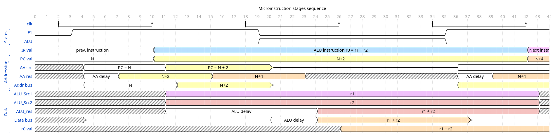
3 days ago • 0 commentsThe last time I made update to FSM design, it turned out working ok. But, returning to it now, I find that there is still room for improvement, especially regarding overall sequencing of micro-instruction stages.
The overall sequence is as following: at the falling clock edge a new state is entered, and appropriate signals for selectors, bus drivers and register addresses to be written (write enable lines) to percolate through combinational logic circuits. Then, at the rising clock edge, all the registers (which have their write enable signals HIGH) get new data latched. Regarding data processing, as in example below for ALU instruction: the instruction itself has several bits that are used almost directly to set the ALU to do what instruction says, so the operation begins when there is still Fetch state. This gives time until next rising edge for it to output its result. On the other hand, between starting memory access operation (fetching instruction) and latching the value there is only half a cycle, which makes addressing very constrained by time available. The other half cycle for memory access is idle.
Here is the example timing diagram showing this:
![]()
------------
I think, there is a way to make memory access time a full cycle, with moving setting of the select and enable signals at the rising edge. This will make them seem to be at the same time as latching, but in fact, the latching will be for values from previous micro-op, and there will be delay between rising clock edge and update to select/enable signals because they will be delayed by intervening combinational logic.
----------
This, along with tweaks to ISA prompts reevaluation and new update to FSM, on which I am working now.
-
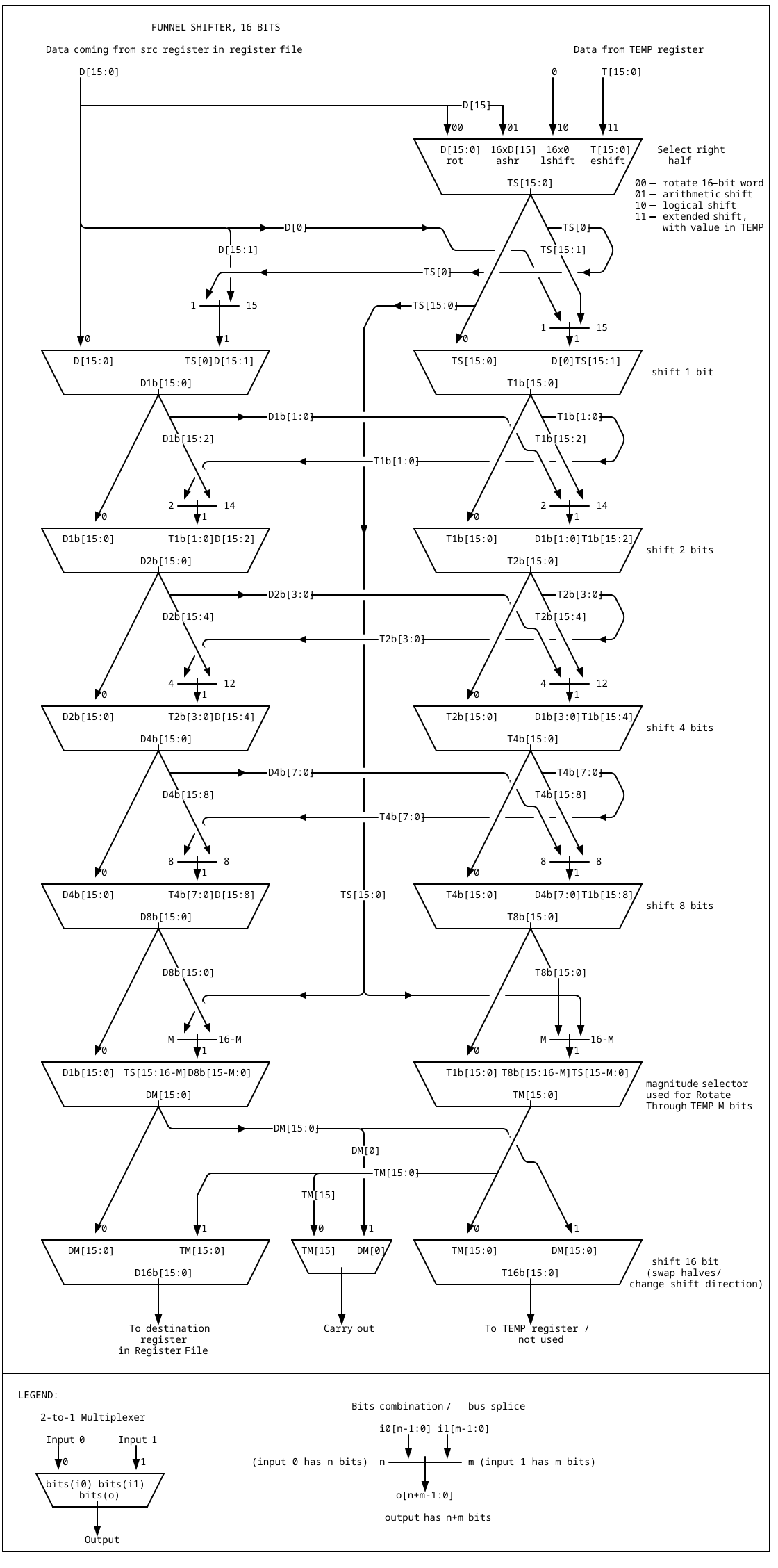
Funnel Shifter 16-bit diagram
7 days ago • 0 commentsI had scaled up the model shifter described in previous log to the full 16 bit width. Along the way I found some inefficiencies in design, and corrected for them -- this made circuit to behave slightly differently in marginal ways, but overall change is positive due to some irregularities weeded out. This is mostly theoretical for now, as the circuit exists mostly as various diagrams I drawn while designing it; also I created the Verilog description, flashed it onto FPGA and tested -- it turned out to work correctly.
Here is functional diagram of this circuit:
![]()
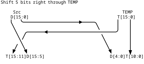
As was written in previous log, this shifter makes use of additional register as source of data, the register is called TEMP, and it is outside of main Register File. This additional register is used only in subset of operations this shifter is capable of, namely, the Rotate Through Temp op (which is like Rotate Through Carry, but extended to several bits at once), and Frame Shift, where a contigous 16-bit field is extracted from combined Src and TEMP registers.
The Rotate Through Temp requires special circuit I called Magnitude Selector. It consists of 2 parts -- the circuit that takes in 4 lines defining rotation amount (1b, 2b, 4b and 8b) and outputs 16-bit value containing from 0 to 15 ones, like this:
0:   0000 0000 0000 0000
1:   1000 0000 0000 0000
2:   1100 0000 0000 0000
...
7:   1111 1110 0000 0000
...
15:  1111 1111 1111 1110
through 16 lines; these lines, each ANDed with enable signal drive the muxes between 8b and 16b selectors. This makes it possible to swap a selected number of bits between TEMP register and shifted bits from Src register; the leftower bits of TEMP stay unaffected:
![]()
This one is the more complex part of this whole circuit.
I am thinking of adapting this design to using 74HC family logic, and juggling between wiring complexity and propagation delays, I think at least the last 3 stages should be condensed into one consisting of 8-to-1 muxes (74HC151). This seems more appropriate, as each bit should be switched separately for magnitude selection, and the 2-to-1 muxes (74HC157) are packaged in a way that switches 4 muxes by single select signal.
------------------
Although almost all diagrams I hand drawn, I found a cool website (with editor called svgbob) which turns ascii diagrams into svg images, facilitating line drawings. So the diagrams above were done using it.
-
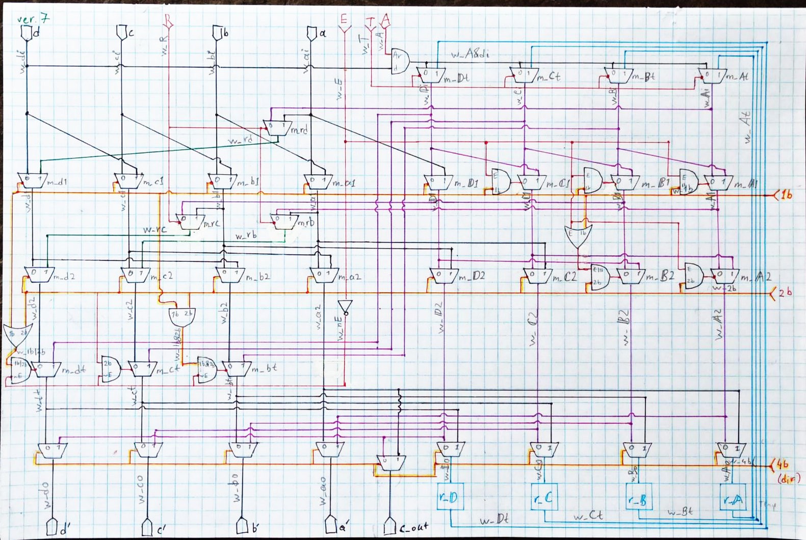
Funnel Shifter (4-bit model)
03/13/2026 at 17:52 • 0 commentsIn previous post I wrote about planning to add a funnel shifter (an extended barrel shifter) to this CPU design. Now, I have designed a 4-bit prototype, and implemented it in FPGA, it has all the needed control signals, and performs all operations I intended it to perform. The 16-bit version would have more bits controlling shift amount, but other control signals will stay the same.
What is the Funnel Shifter?
This is an extension of the Barrel Shifter, in a sense that it is 2 times wider than machine word (barrel shifter usually is the same width as word), and can manipulate data on 2 consecutive registers as if was one double-sized register, and extract the arbitrary word-sized bit field. Thus, it takes two words as input, and outputs a single word. In my implementation, there are some additional functions, and caveats.
Here is the schematic I drawn (it is final, 7th version), which helped me in writing Verilog description:
![]() On the schematic, there is the funnel shifter itself, comprised of a bunch of 2:1 muxes with a little sprinkling of AND and OR gates, as well as temporary register represented as 4 data flip flops r_A through r_D (blue squares). This register holds shifted-out bits that could be retrieved later, with special MOV operation, or used in consecutive operation to facilitate multi-word shifts/rotates.
On the schematic, there is the funnel shifter itself, comprised of a bunch of 2:1 muxes with a little sprinkling of AND and OR gates, as well as temporary register represented as 4 data flip flops r_A through r_D (blue squares). This register holds shifted-out bits that could be retrieved later, with special MOV operation, or used in consecutive operation to facilitate multi-word shifts/rotates.
There are 5 types of shifting operations this circuit is capable of:
1) regular shifts to the left or right;
2) arithmetic shift right;
3) rotate word right;
4) rotate through N bits of temp register*;
5) rotate double word.
*This is expansion of Rotate Through Carry, but can use several bits from temp register.
There are 4 control lines defining general operation (red, with inputs on top):
A: Arithmetic shift;
R: Rotate (for single-word rotation);
T: Use the Temporary register;
E: Extended rotation (rotate double-word, has effect only with T).
There are also 3 control lines (golden-red, with inputs on the right) defining shift amount and direction (1b, 2b and 4b).
The temporary register is supposed to be updated only for operations that have T signal high.
As there are 4 control lines, there is 16 possible combinations, but not all of them are useful, and some of them are functionally duplicates. Out of them, 5 combinations are selected to provide 5 operations listed above. Of these, arithmetic shift and single word rotations need to be only to the right.
Rationale for using special temporary register instead of second general purpose register:
there is just not enough bits in instruction for encoding second source register address. I need to provide the source, the destination, and shift amount (or third register containing shift amount), and this is already 9 or 10 bits out of 16-bit instruction, 6 bits that are left are opcode. There is no way to have another 3 bits for yet another source register address.
With global structure of this shifter proven on 4-bit model, the next now is to scale it to 16 bits. -
Plans for the near future
03/07/2026 at 09:08 • 0 commentsI already received my first FPGA board - Tang Nano 9k (it is presumably the best in terms of bang for the buck, with more than 8 thousand LUTs for slightly less than 20 USD, including shipping). The board itself is fairly small and have just a pair of buttons and 6 leds for user interaction, as well as fair number of pins. To have a more hands-on experience, I decided to make an extension board for it, which could also serve as test harness for CPU components implemented with this FPGA.
And I already started my journey into Verilog, making small projects utilizing the prototype extension board mentioned above.Now, to the CPU itself -- I am now working on some updates to ISA after a closer look of what I have to date. Mostly updates are concerning with redoing bit shifting circuitry, and some slight bit rearrangements in encoding the instructions for more clarity.
I am also thinking about addressing, mostly if there is a need of making it 32 bits. In theory such big address space is good, but given the target speed and just physical availability of SRAM ICs, it looks like 24 bit for addresses would be enough (16MB). This also will make Address Adder narrower, and overall somewhat more manageable wiring for Address Unit. Implementation in FPGA somewhat relaxes this restriction, but I still want to eventually make the real physical processor using discrete logic chips, and this phase of implementing it on FPGA should strive to resemble the intended form as close as possible.Regarding shifting operations -- in current design there is a shifter circuit that can do 1-bit shift operations, and barrel rotator that is able to rotate bits in word to arbitrary amount in range 0..15 bits. The rotator was an afterthought, and was added mostly because there were unused slots in selector for ALU operations. The functionality and usefulness of this arrangement is questionable. Thus, returning after the years I had not had an attention to this project, I saw an opportunity of improvement in this regard -- to fuse shifter and rotator into one more complex circuit -- the Funnel Shifter, as I found afterwards it is called. This should be able to make arbitrary shifts and rotations in one cycle, and with additional temporary register there is possibility of extending these operations to multi-word shifts / rotations.
Right now I am working on designing it, simulating, and this will be the first CPU part to be implemented on the FPGA.Afterwards I plan to build up the decoder FSM, ALU, registers and the rest of the CPU; It seems like this whole CPU can be mapped / implemented on the FPGA chip I have with room to spare, so in the end I will have a piece of functional hardware with which I can play further. The Verilog code I intend to write will also serve as blueprint for building with actual logic chips.
-
A small update
02/01/2026 at 07:06 • 0 commentsDue to life's circumstances, I haven't been able to pursue this project as it is for the last 4 years, and it seems I won't be able to do so for a while yet.
The dream of building my own CPU is not dead yet, so there will be a follow up on it soon (I hope).I found out recently there are inexpensive FPGAs available on AliExpress, so I've ordered one (Tang Nano 9k), and plan to play with it, at the same time finally learning Verilog, and then will try to implement architecture described in this project (with some modifications) on it. This will provide much more portable solution, definitely cheaper, though not a true discrete component cpu, but still something more tangible than software simulation.
-
Memory map
12/12/2022 at 19:57 • 0 commentsThe computer has 32-bit address bus, which provides address space of 4 Gigabytes of memory. This is quite big, taking into account that processor will run at frequencies in range of megahertz. It will take more than half an hour for PC to traverse from address zero to the top of this address space doing only NOPs (they take 2 clock cycles) when running at 4MHz. This is impractical in my opinion. Also, as I intend to use SRAM chips, it will be very big and very, very expensive build, which may not even be capable of work at such speeds reliably.
So there will only be maximum of 16 Megabytes of SRAM (main RAM) installed -- for this only lowest 24 bits of address are needed.
The main RAM address range will be from 0x0000.0000 up to 0x00FF.FFFF. This is just 1/256 of all the address space.
Maybe some time in the future I'll implement some sort of memory management with paging and ability to swap memory to permanent storage, and thus full address range could be utilized.
These 16 MB are the lower memory.
There will also be a chunk of address space where ROMs and I/O is mapped. For future proofing I decided to place it at the very top, in range from 0xFF00.0000 to 0xFFFF.FFFF.
The first megabyte (0xFF00.0000--0xFF0F.FFFF) is reserved for ROMs, where system monitor and standard interrupt service routines are to be located.
The last megabyte (0xFFF0.0000--0xFFFF.FFFF) is for Video RAM -- there 2 video buffers are to be located, they will be switching as described on this section of wiki article (page flipping). The two pages of VRAM will not necessary occupy a whole megabyte, I think that pages 128 kBytes each will be enough. These buffer pages will be on the very top of address space.
The next to last megabyte (0xFFE0.0000--0xFFEF.FFFF) is to be reserved for various I/O ports, video control registers, palette and character table.
All the addresses in between will be left unused, there are just so many of them.
Graphical overview of the whole address space:
+-------------------------------------+ FFFF FFFF
|       ROMs, I/O, video RAM          |  16MB higher memory
+-------------------------------------+ FF00 0000
|                                     | FEFF FFFF
~       No hardware mapped here       ~
~  May be used for virtual addresses  ~
|                                     | 0100 0000
+-------------------------------------+ 00FF FFFF
|             Main RAM                |  16MB lower memory
+-------------------------------------+ 0000 0000
Graphical overview of the higher memory:
+-------------------------------------+ FFFF FFFF
|              Video RAM              |  2 pages 128 kBytes each for display data
+-------------------------------------+ FFE0 0000
|                 I/O                 |  keyboard, PATA, UARTs etc. mapped here
+-------------------------------------+ FFD0 0000
|                                     |  unused
+-------------------------------------+ FFC0 0000
|                                     |  unused
+-------------------------------------+ FFB0 0000
|                                     |  unused
+-------------------------------------+ FFA0 0000
|                                     |  unused
+-------------------------------------+ FF90 0000
|                                     |  unused
+-------------------------------------+ FF80 0000
|                                     |  unused
+-------------------------------------+ FF70 0000
|                                     |  unused
+-------------------------------------+ FF60 0000
|                                     |  unused
+-------------------------------------+ FF50 0000
|                                     |  unused
+-------------------------------------+ FF40 0000
|                                     |  unused
+-------------------------------------+ FF30 0000
|                                     |  unused
+-------------------------------------+ FF20 0000
|                                     |  unused
+-------------------------------------+ FF10 0000
|                 ROMs                |  EEPROMs with system software (monitor, ISRs)
+-------------------------------------+ FF00 0000
|                                     | FEFF FFFF
~          virtual addresses          ~
The ROMs and VRAM will not occupy whole Megabyte slots, but placed individually for ease of addressing.
Graphical overview of the VRAM slot:
+-------------------------------------+ FFFF FFFF
|               page 1                |
|            (128 kBytes)             |
+-------------------------------------+ FFFD 0000
|               page 0                |
|            (128 kBytes)             |
+-------------------------------------+ FFFC 0000
|                                     |
|                                     |  unused
+-------------------------------------+ FFFA 0000
|                                     |
|                                     |  unused
+-------------------------------------+ FFF8 0000
|                                     |
|                                     |  unused
+-------------------------------------+ FFF6 0000
|                                     |
|                                     |  unused
+-------------------------------------+ FFF4 0000
|                                     |
|                                     |  unused
+-------------------------------------+ FFF2 0000
|                                     |
|                                     |  unused
+-------------------------------------+ FFF0 0000
|                                     | FFFE FFFF
~                 I/O                 ~
The video buffer pages are on the topmost ranges.
At any time one of them is used by GPU, or VGA adapter (yet to be designed and built), and the other can be written to by CPU. When the write is done, and right before new frame is started to be drawn on screen, the pages flipped (with the use of small interrupt service routine), and new frame can be composed on fresh page.
This way, the CPU is decoupled from the harsh VGA timings, and can do its things at its own pace.
Graphical overview of the I/O slot:
~                VRAM                 ~
|                                     | FFF0 0000
+-------------------------------------+ FFEF FFFF
|                                     |
|            VGA controls             |
+-------------------------------------+ FFED 0000
|                                     |
|               UART 3                |
+-------------------------------------+ FFEC 0000
|                                     |
|               UART 2                |
+-------------------------------------+ FFEA 0000
|                                     |
|               UART 1                |
+-------------------------------------+ FFE8 0000
|                                     |
|               UART 0                |
+-------------------------------------+ FFE6 0000
|                                     |
|           PATA interface            |  to be used with CompactFlash storage
+-------------------------------------+ FFE4 0000
|                                     |
|           keyboard input            |
+-------------------------------------+ FFE2 0000
|                                     |
|           terminal output           |
+-------------------------------------+ FFE0 0000
|                                     | FFDF FFFF
~               unused                ~
The devices may change.
For each device/port there reserved quite a lot of address space, but in reality the whole range will be treated as single address, the lower bits will be discarded. This is done to make addressing circuitry easier, and I have a lot of address space to spare.
-
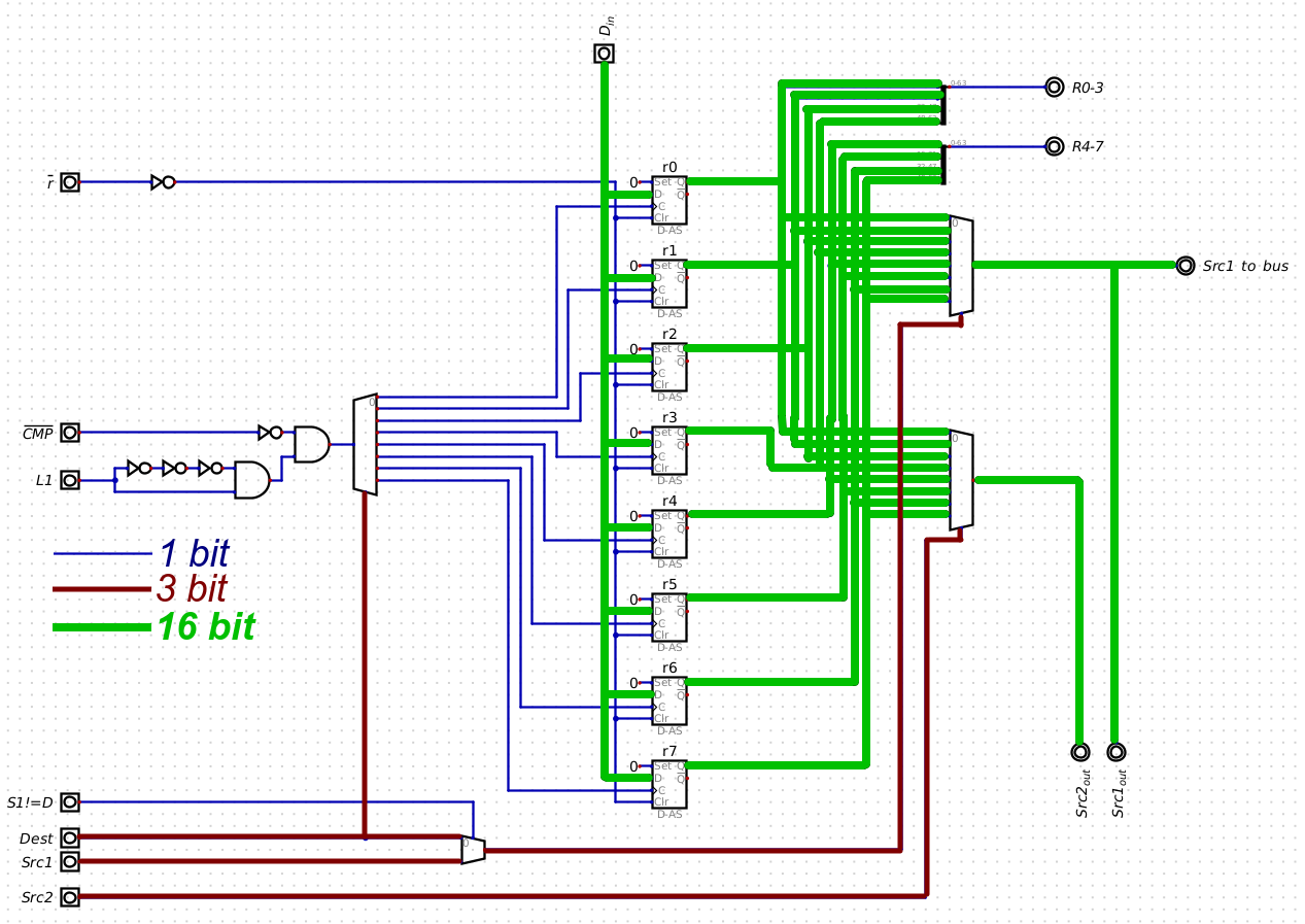
Rethinking multiplexed outputs
12/06/2022 at 07:12 • 0 commentsThere are several 8-to-1 and 4-to-1 multiplexers around the build, which are routing 16-bit and 32-bit wide signals. Managing all this wiring looks like a challenge (one have to look at the Pilot-1 CPU, which is mostly a register file coupled with ALU -- it is ribbon cables all around.
There are quite a lot of wires criss-crossing the 8-to-1 multiplexer boards. It helps that these wires are all individual, and 3-d space allows to weave them as one pleases.
Here is the example schematics for Register File, there are a LOT of 16-bit paths:
![]()
If I to replicate such structure on PCB, turning these wires into traces on 2 planes, it seems that there will not be enough space, and I'll need multi-layered PCBs which are more complicated and expensive to order, and if there some wiring bug in buried layers, there is no way to repair it.
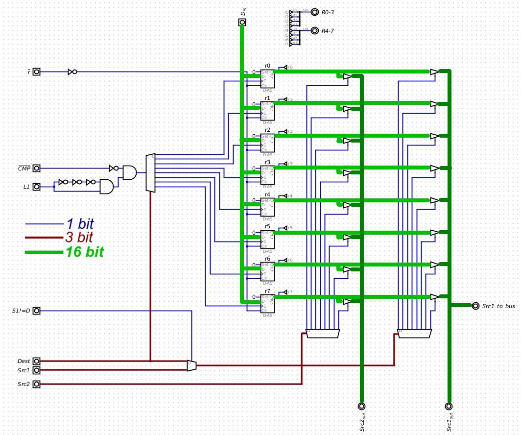
The better solution, it seems, would be to replace multiplexers with tri-state buffers that feed into common bus and activated by single 3-to-8 decoder. This must greatly simplify the build.
Revised schematics for Register File, using tri-state buffers, it looks much more manageable:
![]()
This new solution will be applied for replacing 4-to-1 and 8-to-1 multiplexers; the 2-to-1 multiplexers are fine as they are, wiring them is not as complicated. This replacement will cut greatly into the number of ribbon cables and weird orthogonal board connections in the final build.
The reason I was vary of using this solution earlier is that I thought it would be significantly slower. But it applies more to situations where the clock speeds are much higher and there are much more such outputs to single bus. In my case this speed penalty looks insignificant.
Also, when actually looking into datasheets, the propagation delays for 8-to-1 multiplexer and tri-state buffer are almost the same, and my worries were unsubstantiated.
-
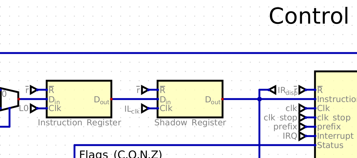
ALU staggering
12/02/2022 at 19:00 • 0 commentsI solved the staggering of ALU execution step and fetch of the next instruction.
The state machine diagram is updated accordingly.
The problem was in timings of propagation delays. All the registers are clocked on rising edge, and the update of gpr and IR should have been at the same exact moment. But in reality, there are several gate delays between rising edge of system clock signal, and the latching of particular register in the register file. On the other hand, instruction register is updated right at the system clock rising edge, thus control signals for the next instruction propagate at the time of latching registers for previous instruction, leading to wrong operation results.
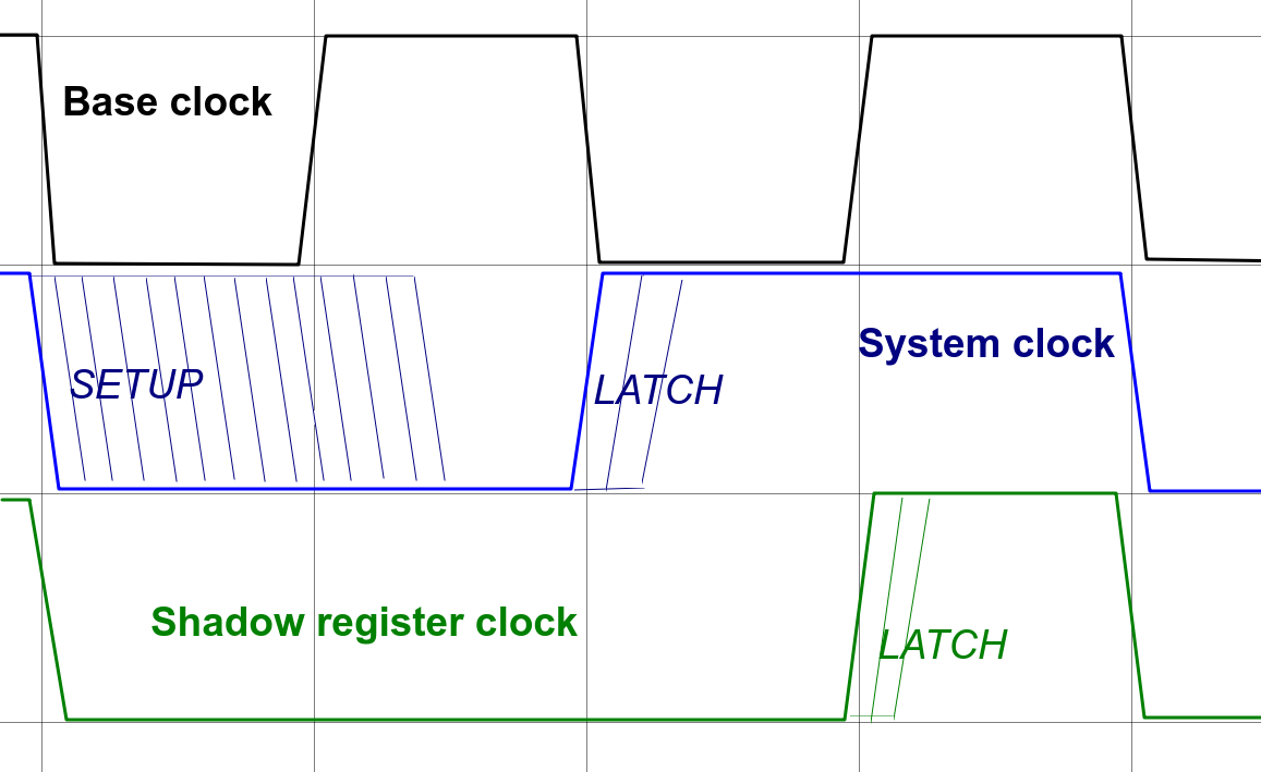
To solve this problem, I introduced "Shadow" register right after the Instruction register, that is latched some time after the IR:
![]()
This new register is clocked with 90 degrees shift relative to system clock, so that instruction word is propagated to decoder a quarter of system clock period later, when all other registers are long latched to their values.
Here is clock diagram for this:
![]()
The system clock is derived from base clock by dividing its period by 2, and Shadow register clock signal is AND between base and system clock signals.
2022-12-06 Update:I figured, there is no particular need to make additional clock phase -- all that needed is a sufficient delay between Instruction Register and Shadow Register latch signals. This can be accomplished by several consecutive NOT gates in the latching signal path for the Shadow Register. While tinkering with simulation, it become clear that delay of just 2 gates is sufficient. In real circuit it may better be done with longer delay, say 6 NOT gates, it will be 20-30 ns.
-
Jumps simplification
11/20/2022 at 18:50 • 0 commentsThe State Machine diagram and Jump instruction layouts are updated.
It looks like there is no need for jumps with offsets in GPR - such jumps are unpredictable at time of coding/assembly, and it is likely that no use can be gained from such an instruction -> removing this option.
Jumps using MPs other than PC as base would be too confusing, and there is also no clear idea what they can be used for -> removing this option.
It seems that jumps with current value in PC as base address are the only useful option -- they are easily predictable.
Thus, decode complexity is reduced, and now also there is no distinction between JMP and JSR states, so only one of them remains.
Jumping to absolute address can be accomplished using interrupts, or via direct or immediate load of address into PC register pair or via double-word MOV into this pair.
For JSR, use of PC can be made implicit.
All of the above simplifies the use of jumps in assembly, the instruction will look like this:
JUMP offset
,where JUMP is any of 10 varieties of jump instructions, and offset is the distance from jump address and current PC value.
In practice, the offset is to be calculated by the assembler, and user should use labels.
-
Yet another subproject
11/12/2022 at 17:35 • 0 commentsJust a note: I have created a new subproject for describing the assembly language to use with my CPU, and tracing some progress in development of assembler program.
 On the schematic, there is the funnel shifter itself, comprised of a bunch of 2:1 muxes with a little sprinkling of AND and OR gates, as well as temporary register represented as 4 data flip flops r_A through r_D (blue squares). This register holds shifted-out bits that could be retrieved later, with special MOV operation, or used in consecutive operation to facilitate multi-word shifts/rotates.