Pavel
Pavel-
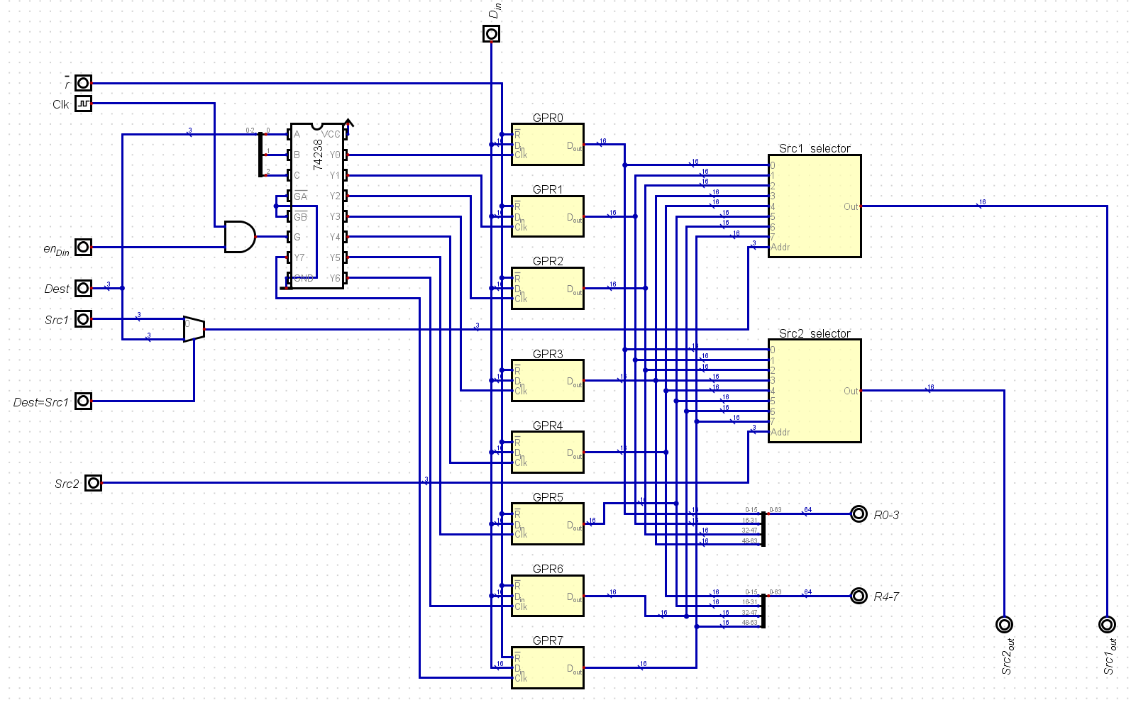
Refined Register Transfer scheme
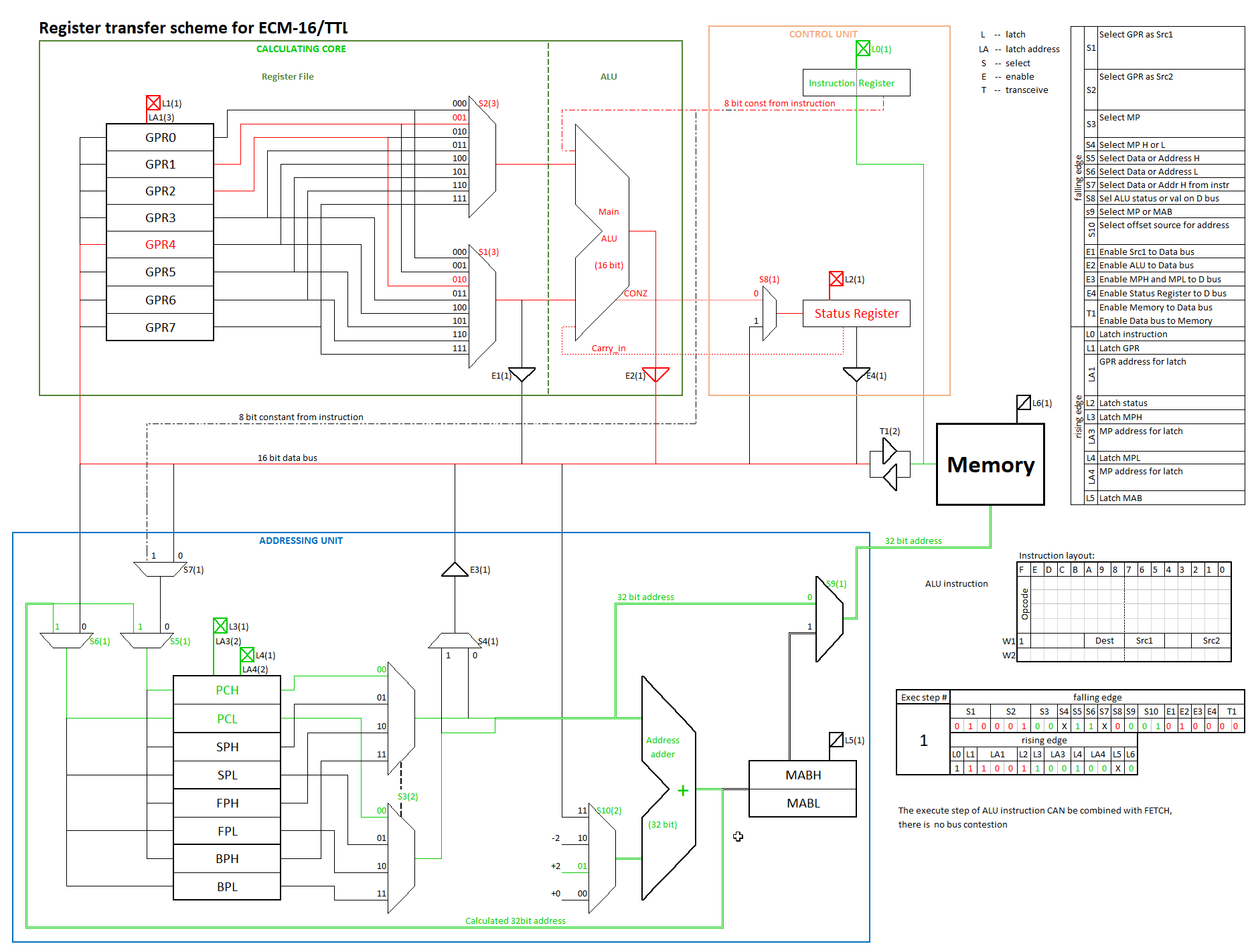
06/21/2021 at 10:15 • 0 commentsAfter starting designing micro-instruction sequences for memory access operations, I encountered some difficulties with the scheme presented in previous log entry. Thus I had to modify this scheme; the modifications were not very big though.
Following changes were made:
1) added 16-bit Memory Data Buffer register -- its primary use is to temporarily store direct offsets;
2) final address source selector was widened from 1-of-2 to 1-of-4, so that all needed address sources are available;
3) added selector of base address source - now base address can be in Memory Pointer, or in Memory Address Buffer -- this is most useful in multi-word data transfers between registers and memory.
Below is the scheme itself, and after it there are some notes about it:
![]()
(By the way, the Excel turned out to be quite useful as line drawing tool for creation of the above scheme)
Register layout and function:
There are 16 addressable registers in 2 blocks, 8 General Purpose Registers (GPR) and Memory Pointers (MP). Each group has dedicated arithmetic unit, for GPR this is 16-bit Main ALU, for the Memory Pointers it is a 32-bit adder.
There is also the 16-bit Instruction Register, which holds currently executed instruction, 16-bit Status Register, which is very special in that its bits can be set and cleared independently, and which is manipulated in its own special way, 16-bit Memory Data Buffer, which is used in some kinds of memory access operations, and 32-bit Memory Address Buffer, which is the source of address in most of the memory access operations.
Busses:
There are 3 main busses --
1 - the 16-bit Main Data Bus, it is used for general data exchange,
2 - 32-bit Address Bus, providing address for accessing memory location,
3 - 16-bit Instruction Bus, that is kind of offshoot of the main bus, but can be cut off, so some register transfers can be combined with the fetching of new instruction.
-
Coming up with clear addressing logic structure
06/16/2021 at 19:54 • 0 commentsFor some time, hardware soldering was put on hold as some different venues, like microscopy, took my attention. But recently, I returned to think about this CPU more globally, and more particularly about memory access operations. This is important, as after finishing the Register File, connecting it to the ALU and a couple of other boards to make a pilot machine, the time will come for actual building of pretty sophisticated memory access circuitry. And this needs some planning, as the way such circuit implemented in the model right now is pretty messy -- I was building it incrementally adding parts and functions to the model on the go.
Following are my thoughts and designing of this subsystem using more top-down approach, which yielded very clear and quite simple solution:
2021-06-10 ... 14
Updated register model
While thinking about addressing circuitry, and how to reconcile all of the different register sizes (8 bit for Hi8 and SR and IO ports, 16 bit for GPR and 24 bits for address pointers), it occurred to me that there is a better approach -- that I should get rid of all these different sizes and go with one size -- all addressable registers are to be 16 bits wide.
In the new config following registers are included:
- 16 addressable registers:
- 8 General Purpose Registers: the 16-bit registers which are connected to main ALU, and which are used for data manipulation;
- 8 Memory Pointer Registers: the 16-bit registers used in pairs to form 32-bit memory addresses (Program Counter, Stack Pointer, Frame Pointer and Base Pointer), connected to 32-bit Address Adder;
- 1 visible(?) special register:
- Status Register, a collection of latches used for holding machine state (Carry, Overflow, Negative, Zero, and Interrupt masks, and possibly other info(TBD)), connected to Data Bus as 16-bit value;
- 2 invisible (background) registers:
-- Instruction Register (16-bit): holds currently executing instruction;
-- Memory Address Buffer (32-bit): additional memory pointer, used in some of the addressing modes.- ??? may be some other registers which I do not know about the need of.
In the above model there is no dedicated Input and Output registers inside the CPU -- all I/O would be memory mapped.
On the other hand, there is now plenty of addresses for all the needs -- actually 4Gig of them. The machine still will have max 16MB of actual installed memory, mainly due to cost considerations, but making virtual memory will be simpler.
For this much addresses the adder will be bigger and more complicated than in the main ALU, due to it being 32-bit, and for it to not be bottleneck for speed, it probably should have 2-stage carry-look-ahead unit.Each of the 16 addressable registers can be loaded and stored to memory. Special instructions may do the same for SR, but with some restrictions (most probably this should be done at function call and interrupt servicing sequences).
The Memory Pointer registers are to be loaded and stored in pairs, as 32-bit values.
Probable extension to loads/stores of several words in one instruction. This will be 1, 2, 4 or 8 words, (may be even 16 words, but there are doubts about this).
Also there needs to be provision for loading/storing individual bytes, will make work with characters and strings easier.Following modes are desired:
0: Immediate load (2-word instruction):
Loading the word right after instruction into a register. There is no corresponding store, as it not useful.
Uses: pre-loading registers with initial data values;
Modified version is a step in direct memory access, when address is encoded into instruction
2 variants: load 16 bits of data, and load 25 (or 24) bits of address1: Direct loads and stores at address encoded in instruction (2-word instruction):
Thus address ranges 0x00000000-0x00FFFFFF and 0xFF000000-0xFFFFFFFF are accessible.
(Accessible address ranges would be 0x00000000-0x007FFFFF and 0xFF800000-0xFFFFFFFF if 24 bits of address could be loaded.)
Bottom part is reserved to RAM, while top part is for ROM and I/O.2: Loads and stores at address in Memory Pointer, with offset of up to +-32767 bytes (1-word or 2-word instruction):
Full 4Gb of address space is accessible, Virtual Memory need to be implemented for full use.
This is the mode for regular memory accesses.3: Loads and stores at address in Memory Pointer, with post-increment/decrement (1-word or 2-word instruction):
Data is accessed at address in Memory Pointer, same as (2) and the Memory Pointer value is updated.
To be used in loops and stack operations, also for simple memory access without offset when post-increment value is selected to be 0.
This is the mode for regular memory accesses, more restricted but faster than one with offset.4: Loads and stores at address in Memory Pointer, with pre-increment (1-word or 2-word instruction):
Value in the memory pointer is updated, and data is accessed at new address.
To be used in loops and stack operations.Offset value sources:
+0 - hardcoded -- default;
+2 - hardcoded -- used for incrementing PC, and popping words from stack;
-2 - hardcoded -- used for pushing words to stack;
+Data16bit(signed) -- data placed to bus, can come from one of GPR, or from memory, most flexible way of data access;Possible extensions:
6: indirect access (by reference in memory, the pointer variable) -- probably can be done using combination of the above modes.2021-06-15
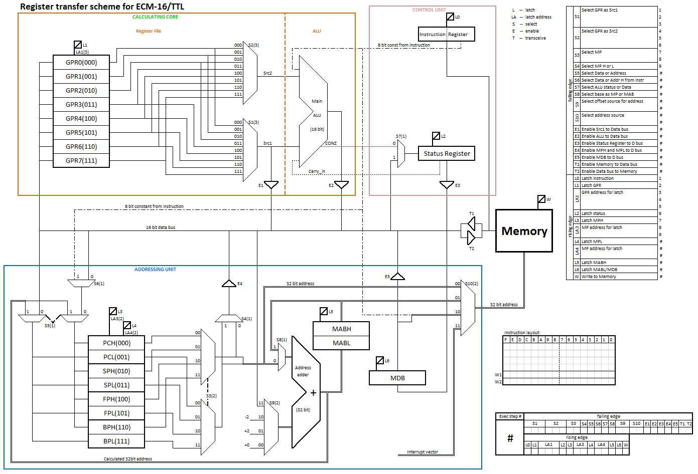
Register transfer scheme for the CPU
I've finished graphical representation of register transfer model, and it looks neat:
![]()
Above picture shows all planned registers with data paths connecting them.
It also shows an example of designing of micro-instructions, in this case an ALU operation, combined with fetching of the next instruction. As, per this model, there is no congestion over any bus, these two steps can be done in one clock cycle, and thus, when there are many such instructions in sequence, they are essentially executed one instruction per clock cycle.
I now wonder why I haven't done this earlier, as it would have clarified so many aspects of my CPU.
This representation will also greatly help in designing micro-instruction sequences for CPU instruction set, specifically ones involved in memory accesses.
Regarding these instructions, I am confronted with scarcity of instruction word bits for assignment of instructions, and therefore part of what I want cannot be implemented because of this. Time for tough choices had come.
It is unclear to me if I really need instructions for accessing single bytes of memory. There is a strong perception that unpacking/packing bytes into 16-bit words using main ALU will not be much slower than fetching and storing those bytes to memory one by one. And ALU operations are fastest of all, they are going to be executed effectively at 1 instruction per 1 clock cycle, when in sequence.
Another thing is loading/storing multiple words per instruction: this would be very nice thing to have, as it would make some loads/stores faster, but they are not necessary for CPU to work properly.2021-06-16
Thoughts regarding circumventing instruction word's "bit scarcity"
One possible solution regarding bit scarcity just occurred to me. What about using some sort of presettable flags to modify base instruction? Like having BYTE flag, that if set makes all memory accesses 1-byte? This, and other possible flags for other purposes will fit into Status Register, so no new places to store this information will be needed. It will introduce delays, and one should always be careful to clear it right after need is removed to avoid problems, but it looks like a viable solution. It looks like some kind of "prefix", as it will most frequently used right before memory access instruction (like, 1: SETBYTE; 2: LOAD to RegX from AddrY). -
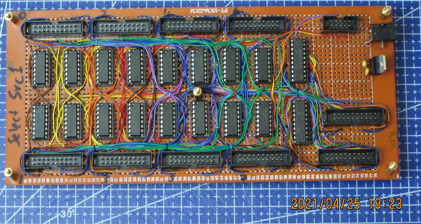
Second RegFile board done (Src1 selector)
04/25/2021 at 17:28 • 0 commentsA quick update on current progress: the second board for Register File is now complete. It is a 16-bit 8-to-1 multiplexer, almost the same as the previous board, only this one has additional 3-state output.
Next will be a "backplane" board for registers. That board will have some logic on it (a couple ICs), and many connectors to which individual small register boards are to be connected.
Here is the photo of Src1 selector board:
![]()
-
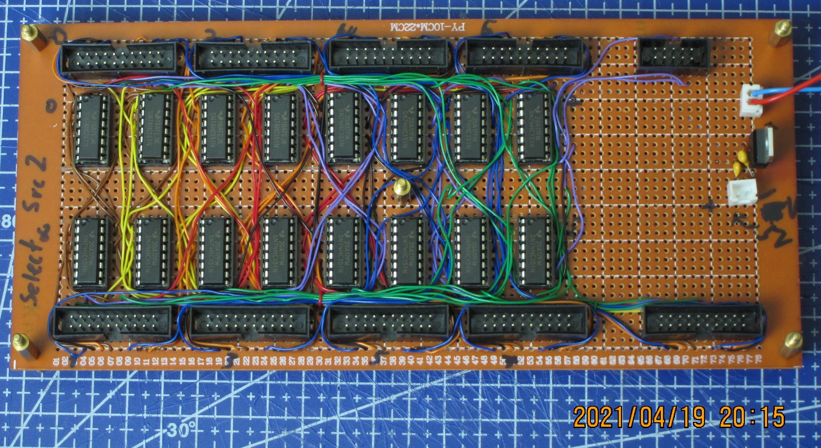
First RegFile board complete
04/21/2021 at 12:49 • 0 commentsThe first board done for the Register File is the selector for the output, which is to be used as Src2 input to ALU. This is conceptually most simple and most familiar part, as the similar board was already been built for the ALU.
Hire is the new board:
![]()
Plans for the future:
Next will be similar board, selector for ALU Src1 input. It will also have additional tri-state output meant to be the output directly to the data bus, which is needed for reg-reg transfers (MOV operations) and for storing data to memory. This independent output from register file to bus, circumverting the ALU is not strictly necessary, but is desirable in view of reducing propagation delays.
On the whole RegFile, regarding creation of single interface board similar to the one for ALU, I think it still an OK idea. I am not yet sure how it will look like, only that it will be integrated with register display.
As for Register Display -- I want to see the contents of all registers at a glance. But not only contents, but also the indication of which registers are selected to outputs as well as to which of the registers is being written. I gather, this has good aesthetics (all the blinky lights) in addition to strictly functional role of being able to monitor and track instruction execution. It could be particularly helpful at the commissioning stage, to ensure all instructions work as desired.
Here is schematic view of what this display is going to be:
![]()
-
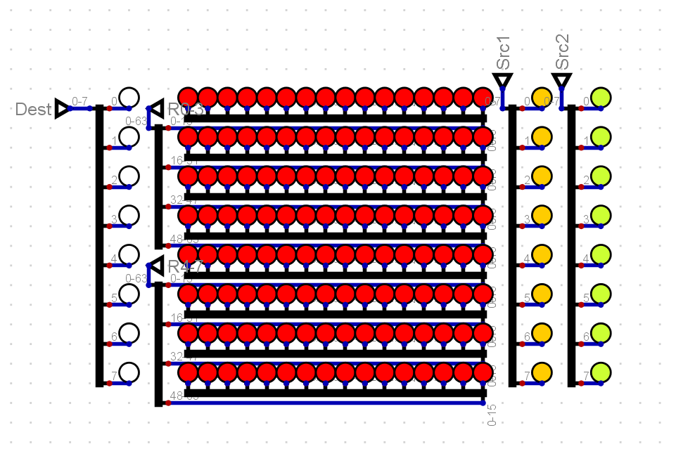
Register File building start
04/08/2021 at 17:54 • 1 commentThis entry is just an announcement of start of building the Register File component (previously described here). It should serve as the statement of commitment.
The Register File will have eight 16-bit registers, and their selection logic.
Here is how I envision its boards arrangement: there would be just 3 big boards ( two 8-to-1 multiplexer boards: selector for Src1 and selector for Src2, and one "RF backplane" board, which will have a handful of chips on it and 8 slots for small register boards), and 8 small boards each having two 74HC273 chips and LEDs indicating content and selection status. The individual small register boards are to be connected to "RF backplane" through pin header connectors.
I am not sure if I need single interface board similar to one I've done for ALU.
Overview schematic of Register File to be built:
![]()
-
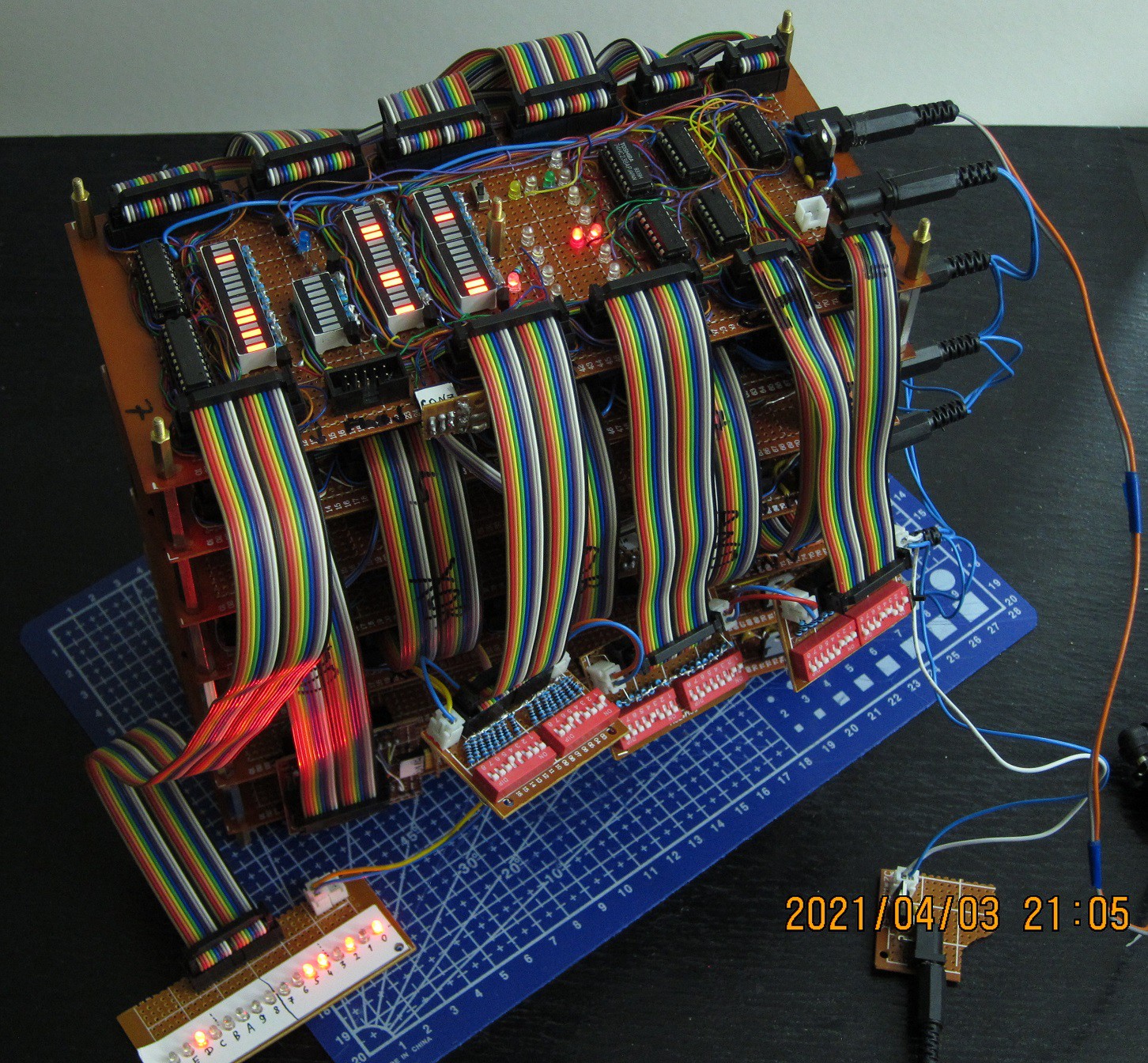
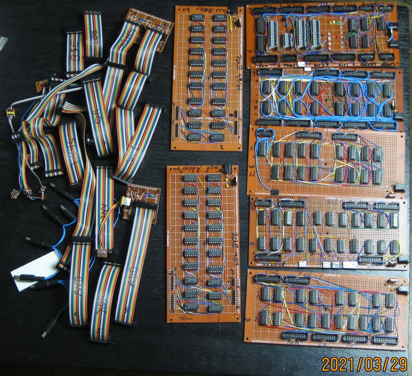
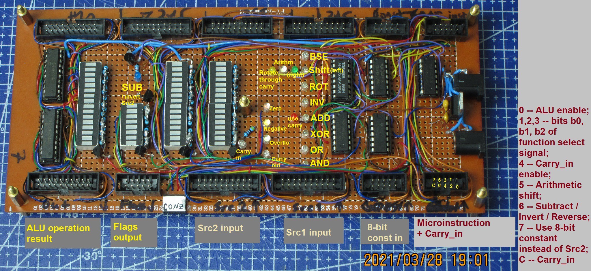
ALU is complete!
04/03/2021 at 20:52 • 4 commentsToday I finished the building of Arithmetic-Logic Unit (with modifications, other modifications, and yet other modifications) for my CPU!
It took almost 3 months, 7 big perfboards and 124 logic chips (logic gates, multiplexers and a couple of bus drivers).
It can operate at up to 5 MHz, and draws up to 200 milliamps of current.
![]()
Description:
List of boards for this ALU (in building sequence):
Fast Adder ( 2 big boards and 2 smaller ones),
Function selector board,
Interface and indication board.
Inputs/outputs
This ALU has five inputs:
1 -- microinstruction, which has 8 lines controlling the operation of the whole ALU:
- ALU_enable line, which enables ALU operation result to the data bus,
- 3 lines selecting one of the eight types of ALU functions,
- Carry_in_enable line (controlling several function flavours),
- Arithmetic_shift line (used only when Shift function is selected),
- Subtract/Invert/Reverse line, which inverts the second operand in two-operand functions, and reverses the shift direction,
- Use_const line, which replaces second operand with 8-bit constant value sourced from instruction;
2 -- Carry_in, which has only 1 line and carries the value of carry_in, used in arithmetic operations;
3 -- Src1, 16-bit, the first operand;
4 -- Src2, 16-bit, the second operand;
5 -- Const, 8-bit , the substitute second operand, sourced from the instruction.
The ALU also has 2 outputs:
1 -- Result, 16-bit;
2 -- flags, 4 lines, the side effects, which are to be stored into status register and used in further ALU operations or in conditional jumps (branch operations):
- Carry_out,
- Overflow,
- Negative,
- Zero.
Functions
This ALU is capable of 8 types of functions most of which have several variants, all operating on 16-bit data:
1: Byte Sign Extend -- simple function which replaces high 8 bits of the Src1 input with copies of bit 7 of this input;
2: Shift -- shifts word given in the Src1 input by 1 bit, has several flavours:
a) shift left (default),
b) shift right,
c) arithmetic shift right (preserves most significant bit),
d) rotate left through carry (msb outputs as carry_out, while carry_in goes into lsb),
e) rotate right through carry (lsb outputs as carry_out, while carry_in goes into msb);
3: Rotate -- rotates the word given in the Src1 input to the left by set amount of bits, has two flavours:
a) rotate using amount encoded into instruction,
b) rotate using amount given by Src2 input;
4: Invert: simply inverts all bits of the Src1 input;
5: ADD (more exactly, instruction which uses the adder), has several flavours:
a) Add value of Src2 to the value of Src1,
b) Add value of Src2 and Carry_in to the value of Src1,
c) Add Const value to the value of Src1,
d) Subtract value of Src2 from the value of Src1,
e) Subtract value of Src2 with borrow (Carry_in) from the value of Src1,
f) Subtract Const value from the value of Src1,
6: XOR, has 4 flavours:
a) Src1 XOR Src2,
b) Src1 XOR Const,
c) Src1 XOR ~Src2,
d) Src1 XOR ~Const;
7: OR, has 4 flavours:
a) Src1 OR Src2,
b) Src1 OR Const,
c) Src1 OR ~Src2,
d) Src1 OR ~Const;
8: AND, has 4 flavours:
a) Src1 AND Src2,
b) Src1 AND Const,
c) Src1 AND ~Src2,
d) Src1 AND ~Const.
9: Compare -- performs subtraction of Src2 from Src1, without saving result to register, only Flags are updated.
Update:
Machine instructions controlling these ALU functions are described in detail in the dedicated project.
Speed
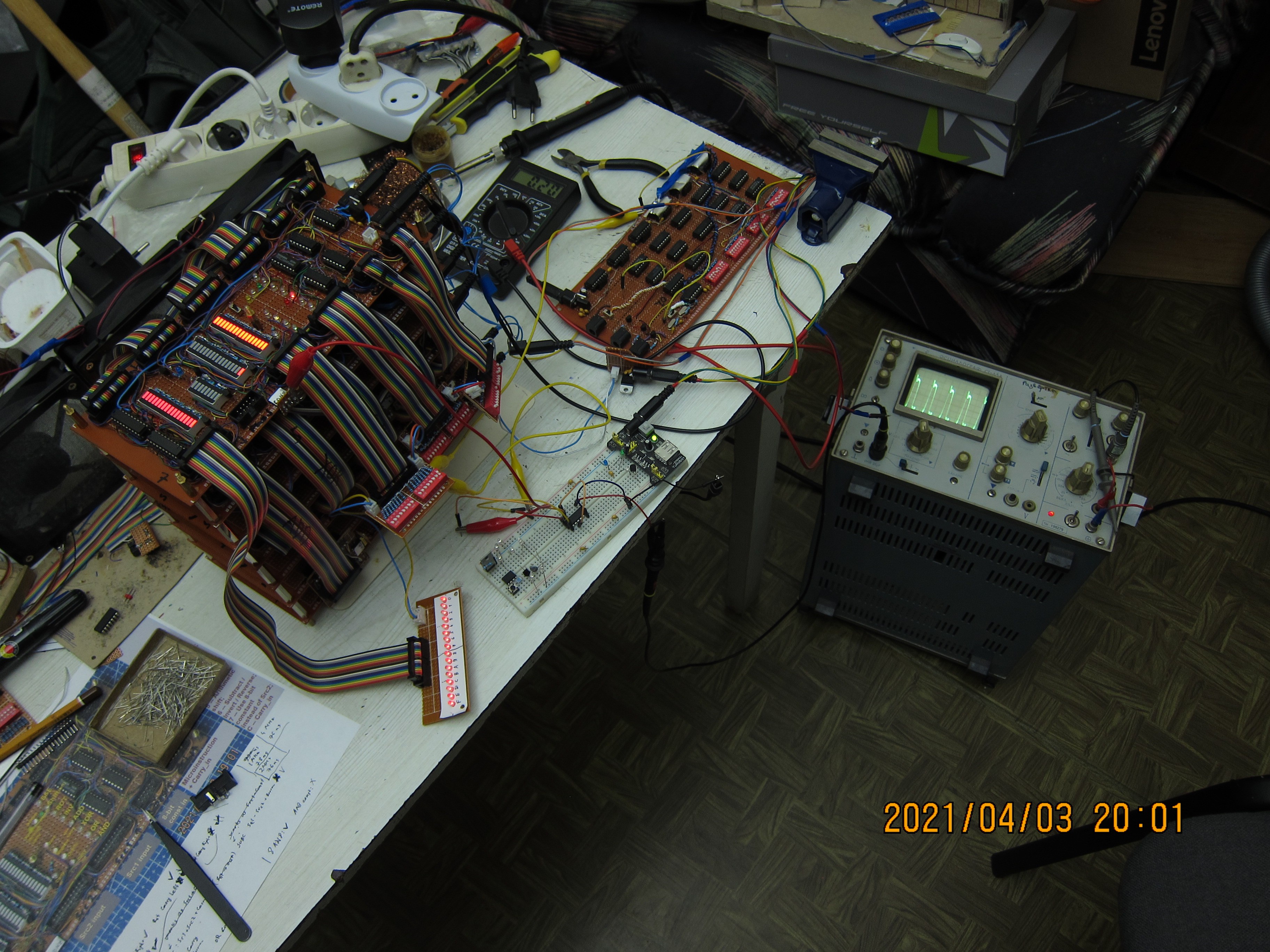
I have measured signal delay of the whole circuit -- well, the worst case delay, or the delay of the longest path, to be exact.
This worst delay is incurred in following situation: when Src1 has value 0xFFFF, and Src2 has value 0x0000 (which is changed to 0x0001), and operation is addition. Measured output is the Zero flag.
On the scheme below it is the path, outlined by orange line:
![]()
The signal change needs to propagate through Incrementor, Negator, Fast Adder ( actually, all 4 four-bit sections of it), function selector and finally, zero detector. As per the model, this is 19 gate delays.
The propagation time was measured to be 76 to 80 nanoseconds, which is consistent with the model and spec gate delays of ~5 ns for HC logic chips. These timings give me hope that the full CPU could operate at up to 5 MHz clock frequency, if ALU operations will turn out to be the longest.
More pictures
(A bit messy) process of measuring circuit delay:
![]()
------------------------------
View from the top:
![]()
-------------------------------------
All of the ALU parts before assembly:
![]()
-
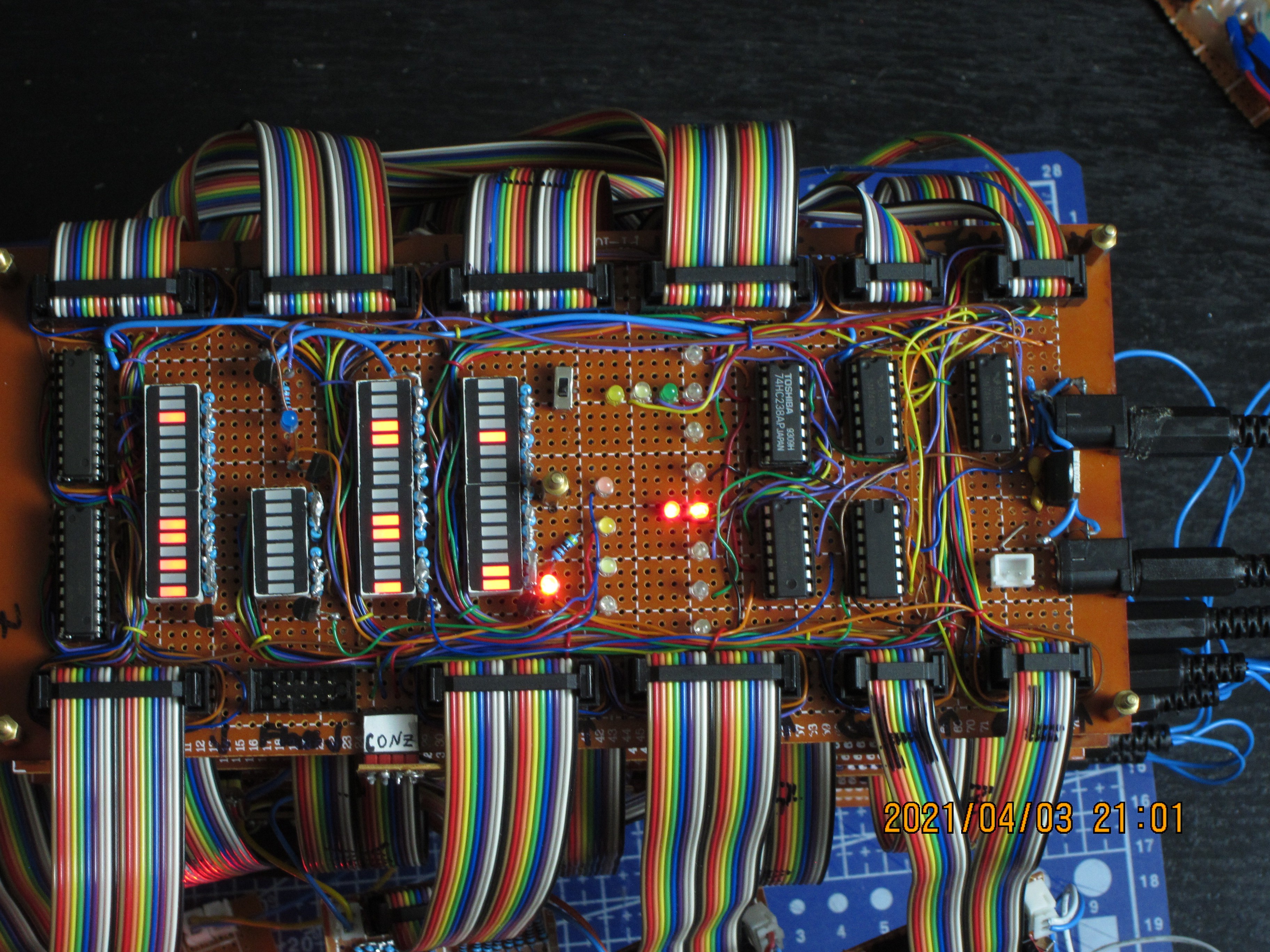
ALU interface board
03/29/2021 at 18:17 • 0 commentsWhen completing function selector board I got the idea to make yet one more board for ALU. This last board should provide a single interface through which the ALU would be connected to the rest of the CPU. Also I hoped that magnitude determination circuit would not be too complex and be able to fit on this board. Turned out this wasn't main concern -- I think, it could be fit on that board with place to spare; the main drawback was long chain of OR gates needed which would make signal propagation big issue. So I opted to have a small function of byte sign extend (BSE) which is just copies bit 7 to all the higher bits.
Instead of adding a complex ALU function to the interface board, I opted to make it a display for the ALU: it has LED banks to show inputs and outputs, as well as individual LEDs to show flags and to indicate which instruction ALU is doing at the moment.
Also the board has bus drivers on result output which make use of ALU enable signal -- if it is 0, the ALU output is floating.
Below is board's photo with captions:
![]()
Next step is integrating all these boards into functional ALU, and testing it out.
-
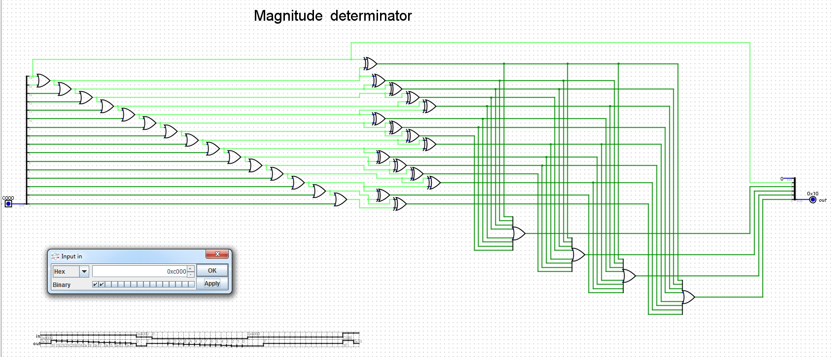
Thoughts on magnitude determinator
03/10/2021 at 08:17 • 0 commentsI finally came up with the circuit that converts 16-bit number into its size (i.e. finding how many bits is the number without leading zeroes).
It has 3 stages:
- first -- make all bits after the most significant "one" bit to be also "one" bits ( like 0001 0110 => 0001 1111 ), using OR gates;
- second -- find an edge with XOR gates -- this turns the 0001 1111 number into 0001 0000;
- third -- encode result from second stage into the final magnitude value ( 0001 0000 => 0000 0101, i.e. there are 5 bits in number );
Here is the schematic:
![]()
One significant drawback here is the long ripple through OR gates, which makes all action up to 18 gate delays long, which is likely one of the longest paths in ALU circuit. This is subject for further investigation right now. Maybe there is a way to make this go faster with fancier wiring.
As for the time being, I am thinking and trying to evaluate, if this circuit is needed at all. It can be most useful in division routine, and maybe also in floating point routines, but I am not seeing this as frequently used feature. All it does can be done with other ALU parts, in several operations.
-
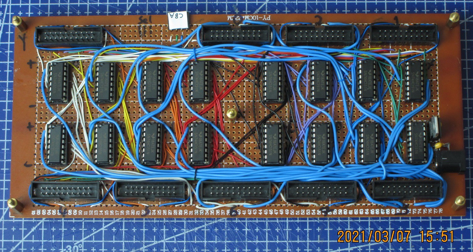
Function selector board; ALU refining, part 3
03/07/2021 at 15:55 • 0 commentsThe function selector board for ALU is completed.
This is 16-bit 8-to-1 multiplexer, using 16 74HC151 chips, and quite a lot of wire.
Here it is:
![]()
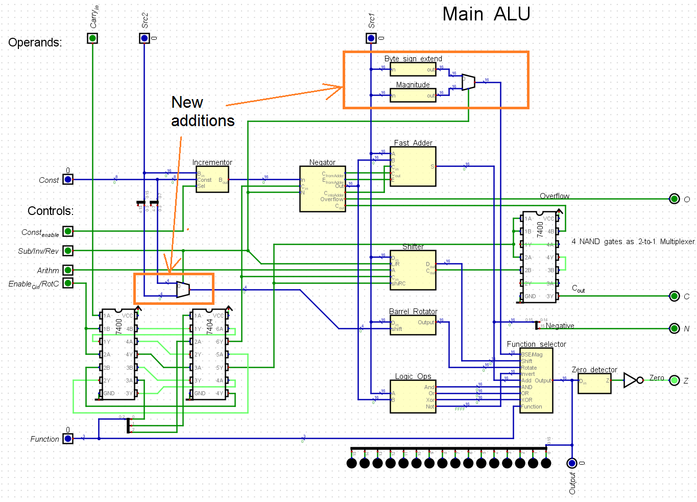
Additional ALU refinements
1. Adjusting ROT instruction:
For now, the ROT instruction can only be used with rotation value hardcoded into instruction itself. Very recently it occurred to me that with a small change (addition of one 4bit 2-to-1 multiplexer) it could be made so that it also can take the rotation value from Src2 register.
The ROT instruction will need addition of one more 74HC157 chip to be modified this way.
2. Replacing ZERO instruction by something more useful:
There are several ways to put zero value into register: could be subtraction from itself, or XOR with itself, or OR with zero, and maybe some other ways. So, having special instruction ZERO feels unnecessary. Therefore, I decided to incorporate some additional functions into the ALU, the Byte Sign Extend (BSE) and Magnitude (Mag).
BSE would just copy bit 7 into all higher bits, making byte values signed.
Mag should give the size of a number in bits, i.e. if there is number 0b 0000 0110 1100 1100 in source register,
the result would be 0b 0000 0000 0000 1011 (the number is eleven bits).
This will probably take one more board, and together with all boards already soldered, fully functional ALU can be assembled.
ALU scheme with updates:
![]()
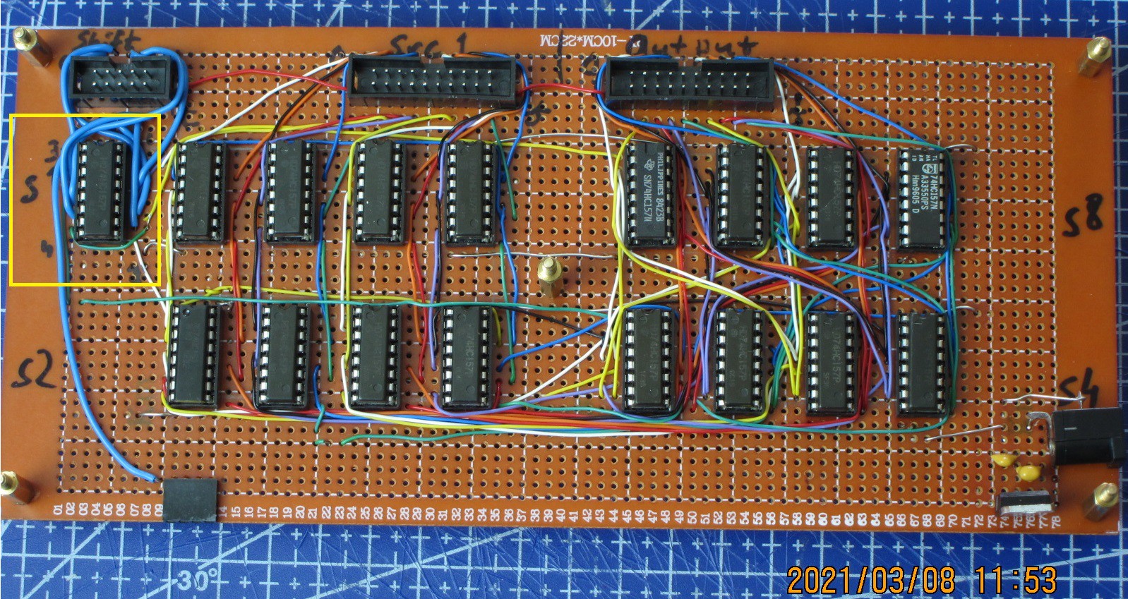
UPD:
1: Rotation amount source selector is added to barrel rotator board:
![]()
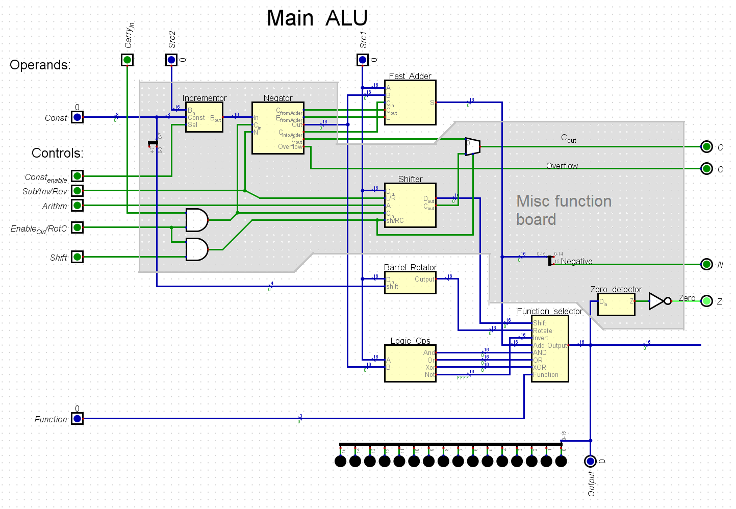
2: Thoughts on scaling back additional functionality:
As I am trying to come up with the circuit that would output number magnitude, it starts to seem that this is a non-trivial task, and such circuit most probably won't be implemented.
So, this would leave only BSE function, which is implemented only by wiring.
-
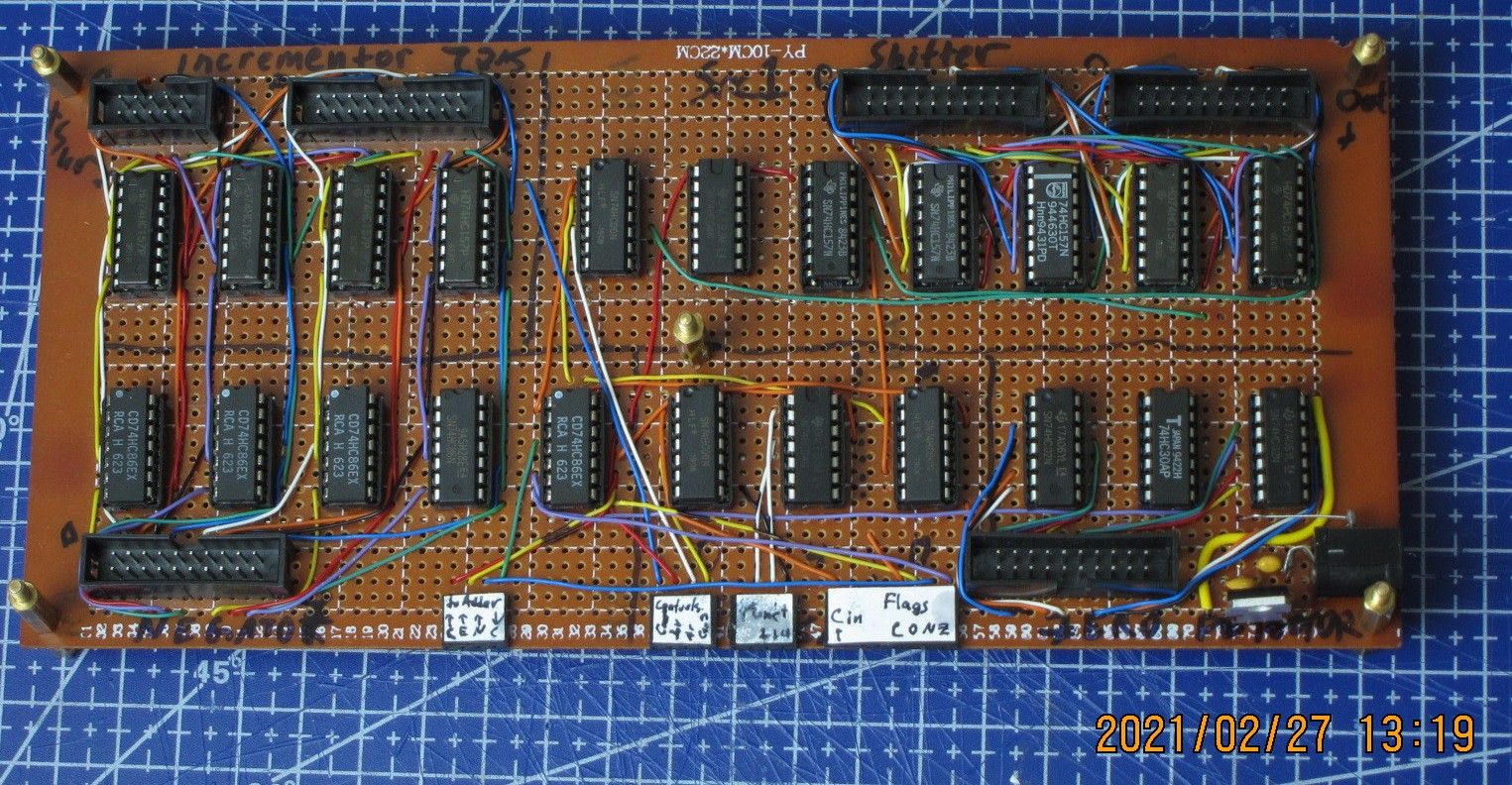
Misc and Barrel rotator boards are complete
03/01/2021 at 08:21 • 0 commentsSince the last update I've soldered , assembled and tested two new boards -- one containing multiple functions, and other - barrel rotator, which performs arbitrary bit rotations of 16-bit words.
Miscellaneous components board
Here is overall scheme of ALU, with components on the Misc board are in shaded area:
![]()
The components take from 3 (zero detector) to 7 (shifter) chips, so all of them were possible to place on single board.
Here is the board itself:
![]()
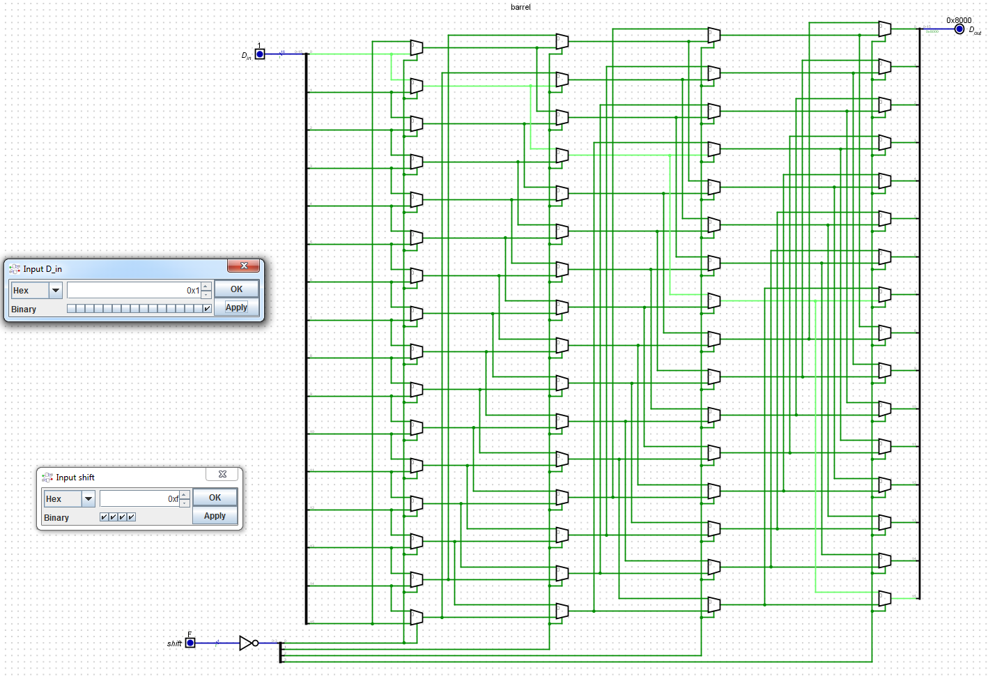
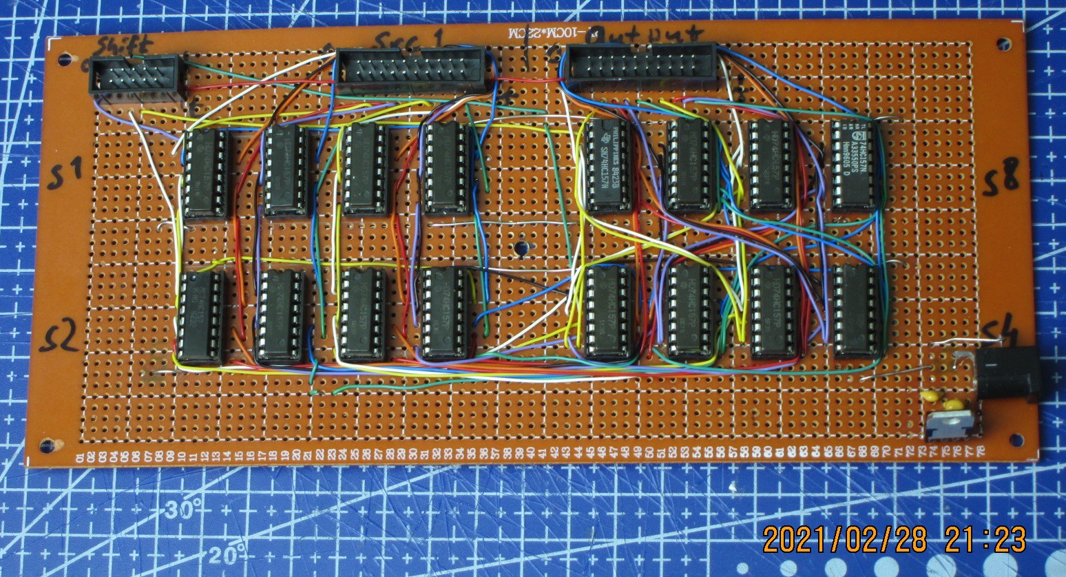
Barrel Rotator board
The barrel rotator performs word rotations to the left by an amount ranging from 0 to 15 bits, in one clock cycle. This module is useful for operations like swapping bytes in the word, or for speed-up of operations involving floating point numbers.
It is constructed as 4 levels of 16-bit 2-to-1 multiplexers, each level multiplexing increasingly disparate bits, here is the schematic:
![]()
and the actual board looks like this:
![]()
___________________________________________________________________________
For ALU completion, only one board is left to be completed -- the 16-bit 8-to-1 multiplexer, which will select one of the outputs from previously created boards.
After that I'll start working on the Register File, and beginnings of the control module.