Pavel
Pavel-
Name for the computer; asm v3
12/11/2019 at 06:48 • 0 commentsName of homebrew computer
I am not good at coming up with names, but after some thinking I've came up with the name for this computer at last:
from now on it will be called ECM-16/TTL. This is itself a quite generic name, meaning Electronic Computing Machine, 16bit, based on TTL logic chips (of 74HC family). A quick search on Google haven't returned such name for any other homebrew computer/cpu, so I claiming this name for my machine in development.Assembler development
On the assembler front, it is now a version 3, and becoming a treat to use, as now it supports labels and directives (though, no expressions yet). The constant reference for bit patterns of instructions and hand-calculation of jump and load/store addresses are no longer needed, all is done automatically.
During development of this assembler, several bugs were found in it, and also in the wiring of computer itself. Now, they are fixed.
There are some things that are yet to be added to the assembler -- I think, adding support for at least rudimentary expressions (like adding constant to label) will be handy. I also thinking about adding of PC-relative addressing for short jumps and load/stores, this way awkward situations on the page and block boundaries could be avoided. But this means adding another adder to machine, this time to addressing circuitry, the thing I've tried to avoid from the very beginning. Also, the assembler logic will have to be changed a bit.
Descriptions on some of the aspects of ECM-16/TTL:
Reason for 24-bit addresses
At first, I was content with having 64k words for this computer design.
But after a while, when designing memory access instructions, I faced the situation: the address must be somewhere. The 16 bits for addressing of 64k are comfortably fit in general purpose registers, and such size is comfortable for shuttling around on the main bus. But I wanted instructions which would have the address encoded into them. I already had instructions for ALU with a constant value encoded into them, like ADD aX 0xff, and this scheme can also be employed for addressing. Thus, there is an instruction like LD aX [0xff], and it is laid out in instruction word as [high byte][low byte] => [opcode][address]. But this only can address 256 words (what I call a single "page") of memory, which is far from desired 64k words. To have an instruction which have in itself the whole address, it itself will be longer than the word. Naturally, it would take up the two words, as this design does not support byte addressing. So, I had 32 bits to play with. One way could be done as [opcode][high8bit of address]:[low8bit of address][not used]; but it would be too awkward to implement in hardware. Another way could be [opcode][not used]:[high8bit of address][low8bit of address], which is much more natural in this design. Now, though, I have 8 bits more than I have to to address 64k locations, so why not use it? Let's define block of memory as 64k locations which can be addressed by one 16 bit word. Then if we use the byte right next to opcode, then it will be the block index, with up to 256 blocks possible to address, and therefore 16M memory locations that could be addressed by 24 bit address. In reality, I don't think the computer will ever have as much memory, mostly because it would be relatively expensive (SRAM chips are to be used for memory).Memory space can be presented as hierarchical structure, with levels differing by ease of access (number of clock cycles needed):
Page -- 256 words, which can be accessed with shortest and fastest instructions;
--I am thinking about re-making in-page addressing into PC-relative one, so there close load/store or jump could be made to +-127 memory locations, independent on page/block boundary. This change will need addition of another adder, 24bits wide, so [base + offset] address of location is calculated on the fly. This may also add quite a lot of complexity to assembler.Block -- 65536 words, addressed by value in one of the general purpose registers;
Global -- whole address space of 16777216 words, which can be addressed by two-word instruction, or compound value from two registers.
----------------------------------
Subroutine callsSomehow I thought subroutine call is just pushing PC to stack; but this turned out not all there is to it. As I was thinking trying to devise a way to make the subroutine call as 2 instructions (push pc+1 to stack and jump), it seemed that this cannot be done: either return address was the address of jump instruction, so endless loop ensues, or the pushing of PC is done after return instruction... as the return address is still undefined, this obviously cannot work. After some reading, it occurred to me, that jump and pushing of PC should be done in one instruction. Luckily, I needn't come up with new distinct machine word for this instruction, as I already had a useless one lying around, from jump family: the unconditional skip, or NOP, the opposite of unconditional jump (This was a kind of conditional jump for which no condition can be true). All I had to do is use it and add PC pushing to Jump decode circuitry. As it was, I overhauled all memory access block, re-done it from scratch, so it became more regular in its wiring and easy to decipher. This overhaul haven't changed anything about its function, except adding the Jump to Subroutine instruction. All other operations are still executed the same way as before.
The JSR operation uses the same stack pointer as the regular stack operations, so return address is stored alongside data, and if one is not careful (like popping more or less data than was pushed), the return address may become undefined.
These subroutine calls can be done from anywhere in a program, and recursive algorithms can be implemented.As of now, there is no provision to store stack pointer address to memory. Though this can be useful to have if one needs separate stacks for data and function calls.
----------------------------------
Assembly description:
General
The program takes in a plain text file with .asm extension, parses it finding opcodes, performs assembly and spits out another text file, with .hex extension, which is just a column of 4-digit hexadecimal values. These are directly mapped to machine code of simulated computer.
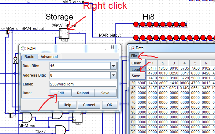
The assembled code is then uploaded to ROM via simulator tools:![]()
Each instruction should be on its own line of assembler program.
The (optional) label, instruction/directive and their operands should all be separated by at least one whitespace character.Instructions
Single opcode can have different sets of operands; depending on particular set used, different operation is performed. The operations are closely related, hence the common opcode. For example, some ALU instructions can have either one register and a small constant, two registers or three registers as operands, which results in somewhat different outcomes. Use of such "overloading" cuts on total number of opcodes in set, which should make it easier to memorize.
Instructions with subscript ( "i" or "g" ) are using up 2 words in memory, all others are using only one.
i - immediate, a one-of the kind load instruction
g - global direct, used for fast and easy access to faraway memory locationIn the following list, instructions are divided into categories by function, and inside categories by type, each type having similar operand lists
Following instructions are supported (46 total):
ALU instructions:
a) ADD SUB
ADDC SUBC
AND ANDN
OR ORN
XOR XNOR
b) CMP
c) SHL SHR
ASHL ASHR
ROLC RORC
d) ROT
e) INVf) ZERO
Memory Access:
a) LDi STi
b) LD ST
c) LDg STg
Jumps:a) b)
JMP JSR* JMPg JSRg*
JC JNC JCg JNCg
JN JNN JNg JNNg
JZ JNZ JZg JNZg*Jump simultaneous with pushing PC to stack
Movs:
MOVStack operations:
a) PUSH POP
b) PUSHPC RETFollowing Directives are supported:
.EQU
.ORG
.END
.BYTE .WORD .DWORD .QWORD .OWORD .HWORDThe mnemonics are heavily influenced by ones presented in book "The Definitive Guide to How Computers Do Math" by the authors of DIY Calculator.
The assembler program, version 3, can be found in "asm3.zip" file in "Files" section. The archive contains .cpp source file, pre-compiled Windows binary and a comprehensive description of assembler and all instructions/directives it supports; also included a small program in described assembly which performs multiplication of two 16-bit values, and displays result on 7-segment display.
There are a couple of unresolved issues with assembler program:
- If there are several whitespaces followed by comment on a line, assembler crashes - avoid such lines
- If the last variable is an array, assembler crashes; workaround -- add a dummy single variable.
The updated version of computer simulation is in archive "computer042.zip".
-
Assembler, first version
11/24/2019 at 13:23 • 0 commentsJust another quick note:
The assembler, first version is created. It seems that it outputs good machine code in hex, which can be then imported into ROM of the simulated computer.
It is not very sophisticated, just converts mnemonics into machine code; there is no support for directives and labels yet.
The source code, compiled binary for Windows, .bat file with commands for compilation of source with g++ and test file are in archive in "Files" section.
On another hand, work on making instruction cycles shorter encountered some problems -- it turned out much more work is needed than I thought at first. For now my attempts were hindered by data/clock races -- next instruction fetches and starts to execute while previous is still in progress, or bus congestion occurs.
-
Small update on simulation
11/18/2019 at 06:47 • 0 commentsTurns out there is still room to some optimisations.
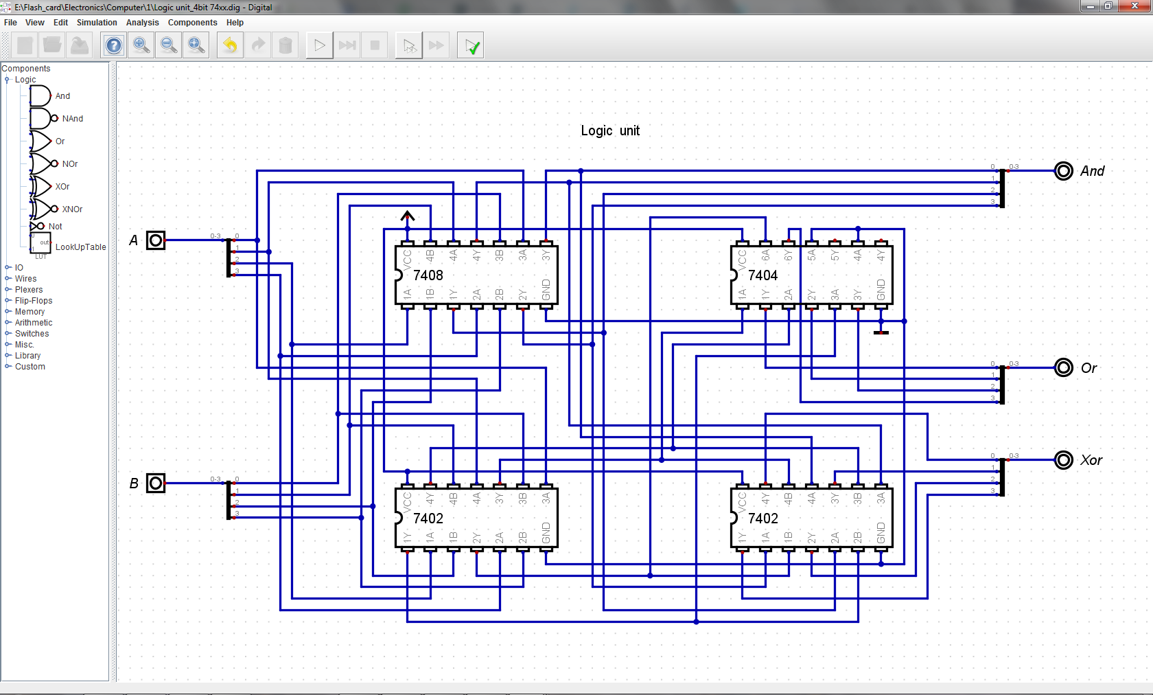
I found a way to squeeze 3rd register address into 16-bit ALU instruction, so now operations on two operands with saving into the 3rd are possible, for example: ADD a0 b1 c2, adds values stored in registers 1 and 2 together and stores result into register 0. This is in no way breaks previous mode where ops were like this: ADD a0 b1, where values in registers 0 and 1 are added and result overwrites register 0. These new operations became possible by slightly changing addressing wiring in Register File. As it maintains compatibility with previous instructions, the new mode has limitation in that only registers 2 to 7 can be used as operand C.
Other changes to ALU operations are made with some modification of ALU itself. The wiring was changed slightly, so one operand instructions (such as shifts) now can store result into other register, without overwriting contents of the source.
Also barrel rotator was added to ALU, which can rotate the word left to up to 15 bits.
The encoding for new register addresses for above operations, as well as for bit number of rotations has been achieved by utilising previously unused bits of instruction (or conditional reinterpret of some bits). This turned out to take surprisingly small changes to ALU/Register File wiring and decode logic.
One encoding which was changed is that +/- bit now is used for shift direction indication instead of previously used dedicated Left/Right bit. All the other changes are additions to previously existing set.
On another note, I found a way to speed up execution to shave off number of clock cycles for some of the instruction types. This is done by staggering instruction execution, so when the last step of current cycle is going on, the fetching of the next instruction begins.
It was possible for instructions which don't do writes to Memory Address Register (MAR) at their last step, so no bus congestion is created.
Instructions affected are ALU, MOV and Load/Store instructions. This way, if they are going in succession, ALU and MOV instructions take only 2 clock cycles instead of 3, and Load/Store operations take 3-4 clocks instead of 4-5, depending on operation.
To achieve this, the changes made were also surprisingly small, 3 or 4 logic gates were added, as well as a couple of wires, to the simulated processor.
The files with updated instruction set as well as simulation can be found in Computer04.7z archive in "Files" section.
-------------------------
Things to add to simulation later:
1. Start-up sequence -- first cycle of 8 clocks nothing is done and Reset applied to whole system, then execution commences with instruction at address 0x000000.
2. Interrupt handling. For now it is still somewhat obscure topic for me.
3. More memory :) For now placeholder is used, with 256 word ROM and RAM. For testing purposes, now it is enough.
-------------------------
Right now I need to write assembler (however crude) in c++, so I won't need to type 0's and 1's in spreadsheet by hand and look up every bit pattern, as it became apparent that this process is incredibly slow and error prone.
--------------------------------------------------------
Quick Update: today it occurred to me that I can make first two steps of instruction cycle into one, by bypassing MAR when doing addressing from Program Counter or Stack pointer. This can be done by rerouting some busses and using two 4:1 24-bit multiplexers instead of one 8:1. So, in coming days I'll try to implement this. It will not change any instruction encoding in any way, but will make all instruction cycles 1 clock cycle shorter. This, combined with recently implemented pre-fetching (described above), will make ALU and MOV operations effectively done 1 instruction per clock cycle in some situations.
-
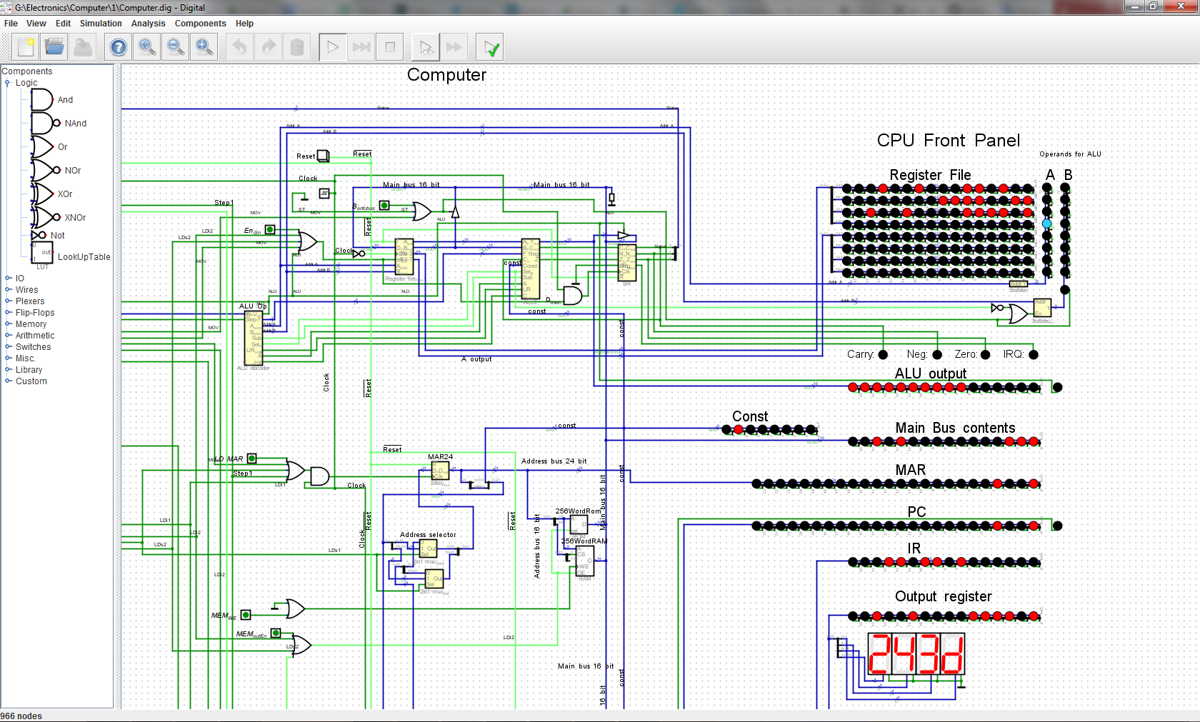
Simulation completion
11/06/2019 at 06:12 • 5 commentsThere was a year long hiatus in my work on this project, but as of recently, I've resumed it.
Looking with fresh eye, I found several things which I hadn't noticed previously, such as commonalities for decode structure in different instructions. This lead to overhaul of decoding circuitry, reducing redundancies while at the same time adding some new instructions ( or rather variations on them ), exploiting found commonalities.
The CPU now is Turing complete. Though there are still possibilities for adding additional instructions, existing set is quite big already.
There are multiple operations for manipulating data with ALU, other ones move data between registers, loading and storing from memory, unconditional and conditional jumps.
The registers are of two types - General purpose (GPR) and Special (SpR). Data in GPR can be manipulated in ALU, while data in SpR can not. Data can be moved between all registers, and also loaded/stored in RAM; although there are some restrictions for particular SpRs.
The ALU can only perform its functions on data from GPRs. Data from memory need to be explicitly loaded or stored as distinct operation.
There is no microcode -- all instructions are decoded by combinatorial logic.
The computer simulation has very rudimentary I/O as of right now.
It also lacks any interrupt handling.
The last two points will be worked on in the future.
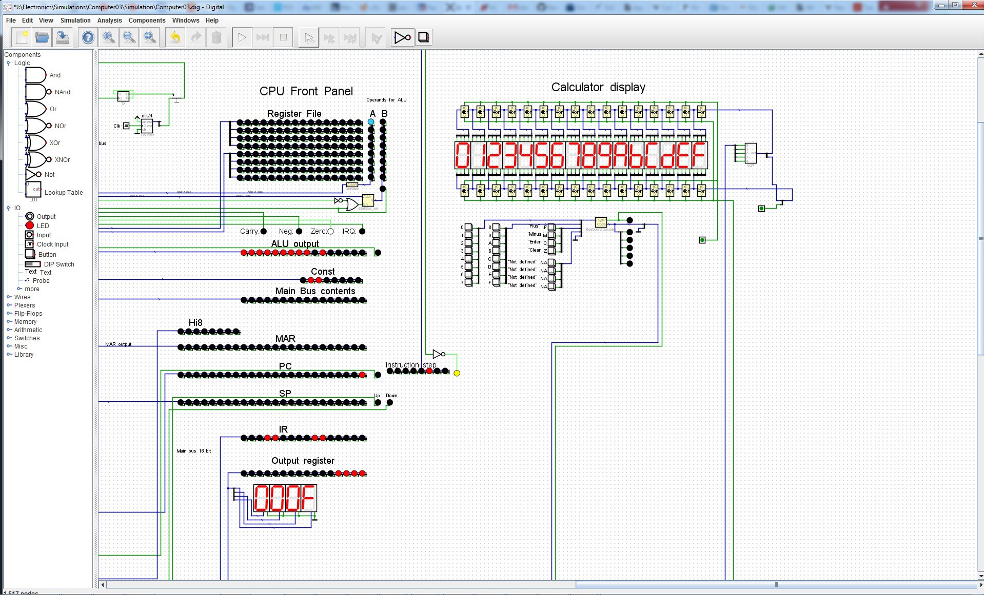
In the Files section there is an archive with simulation files as well as an Excel spreadsheet with all instructions described. It also contains manual "assembler", which makes programming this computer slightly easier.
The simulation files can be opened with Digital logic circuit simulator software.
![]()
-
ALU
08/20/2018 at 07:32 • 3 commentsEDIT: the final, completed in hardware, version of ALU described in newer post.
Original:
This is the description of the Arithmetic-logic unit of this "computer".
Most of it I conceived a year ago, and now, after some modifications, it is one of the most stable parts of the system (along with the register file).
Here is it's inner organisation:
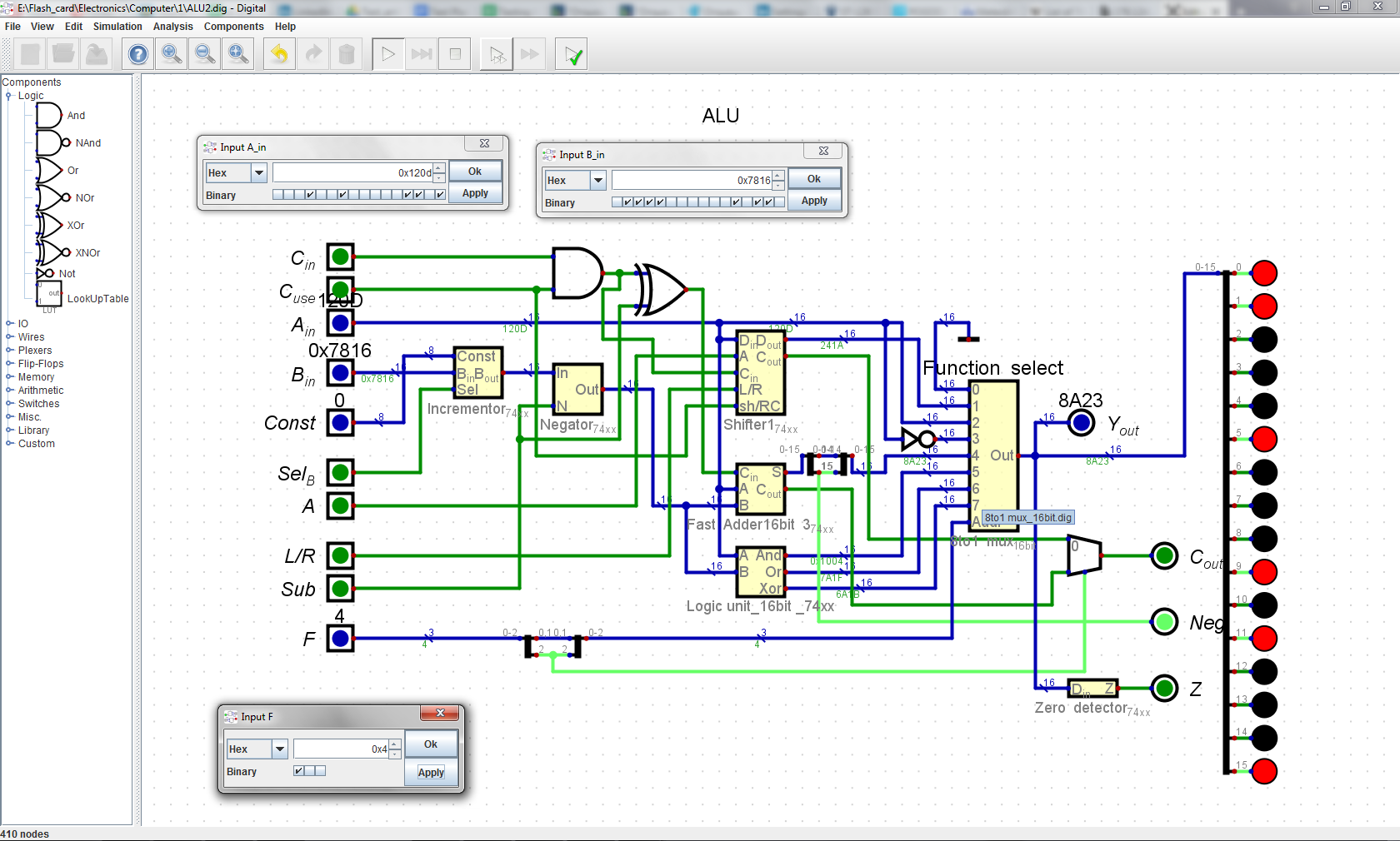
![]()
The ALU accepts two 16-bit operands, A_in and B_in, and outputs one 16-bit value, Y_out, which for ease of debugging is also outputted to 16 LEDs on this schematic.
The A_in and B_in are supplied from Register File, but there is possibility of substituting B_in with some constant value in the range 0 to 255, that is suplied through Const input. Selecting of what is going as B operand is accomplished by 1-bit control line Sel_B through the Incrementor module (just 2-to-1 mux).
Next, the B operand is going through the Negator module (16 parallel XOR gates), where 1-bit control line Sub dictates if B will go further unchanged, or all its bits will be flipped. This same line flips carry bit that goes into adder for facilitating subtraction in twos complement.
On the next stage there are several blocks in parallel, namely, Shifter, Fast Adder and Logic unit.
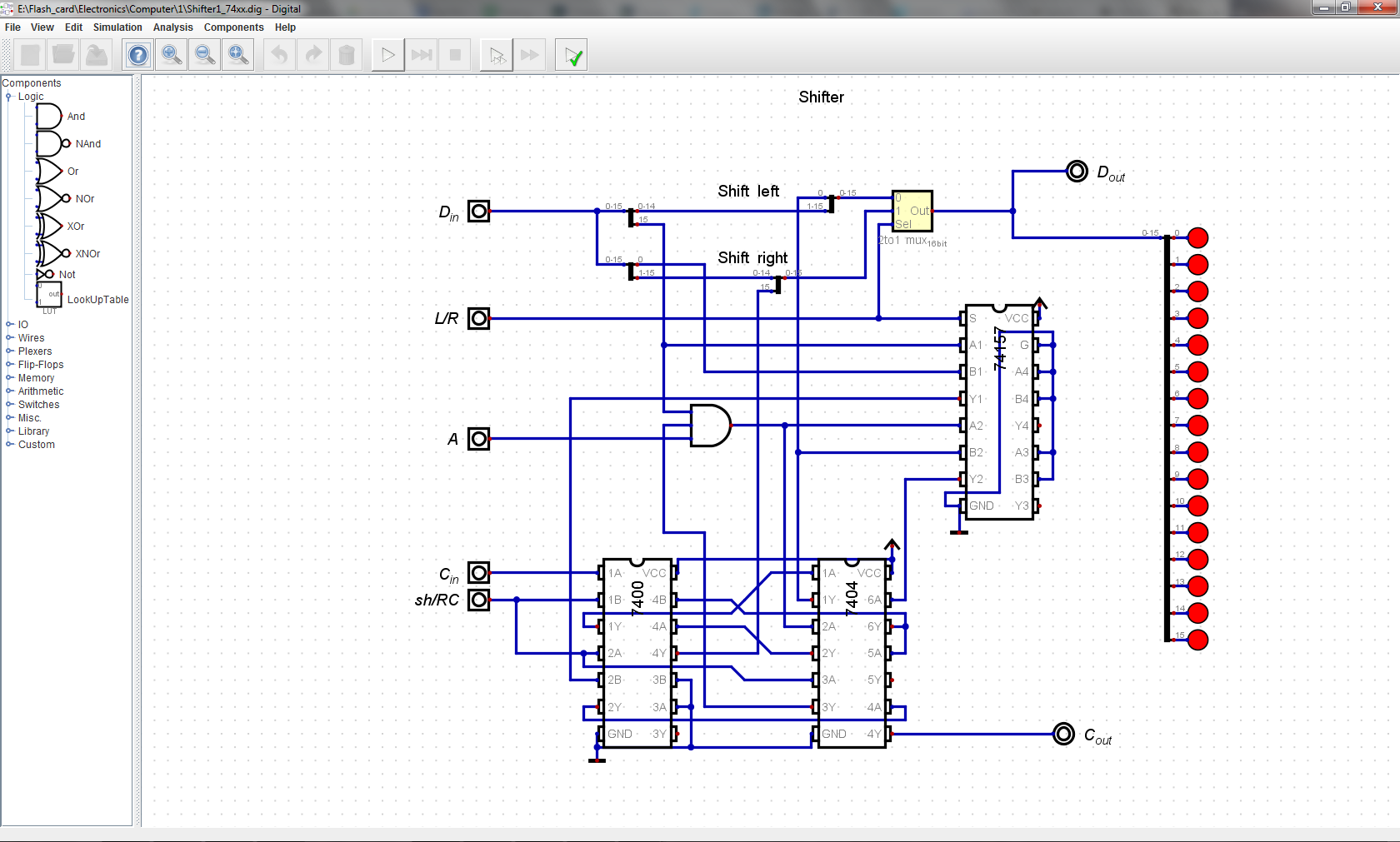
The Shifter works only on A_in operand, so it is ignores whatever is B value. This module takes in 16 bit D_in and 1 bit C_in (carry in) and outputs 16 bit D_out and 1 bit carry out. The three controls are: A - for Arithmetic shift, L/R - for choosing shift direction, and sh/RC, for choosing between Shift and Rotate through carry. The Shifter mostly consists of 2-to-1 muxes with handful of logic gates.
![]()
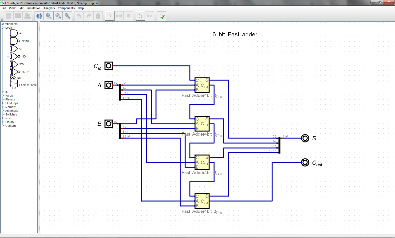
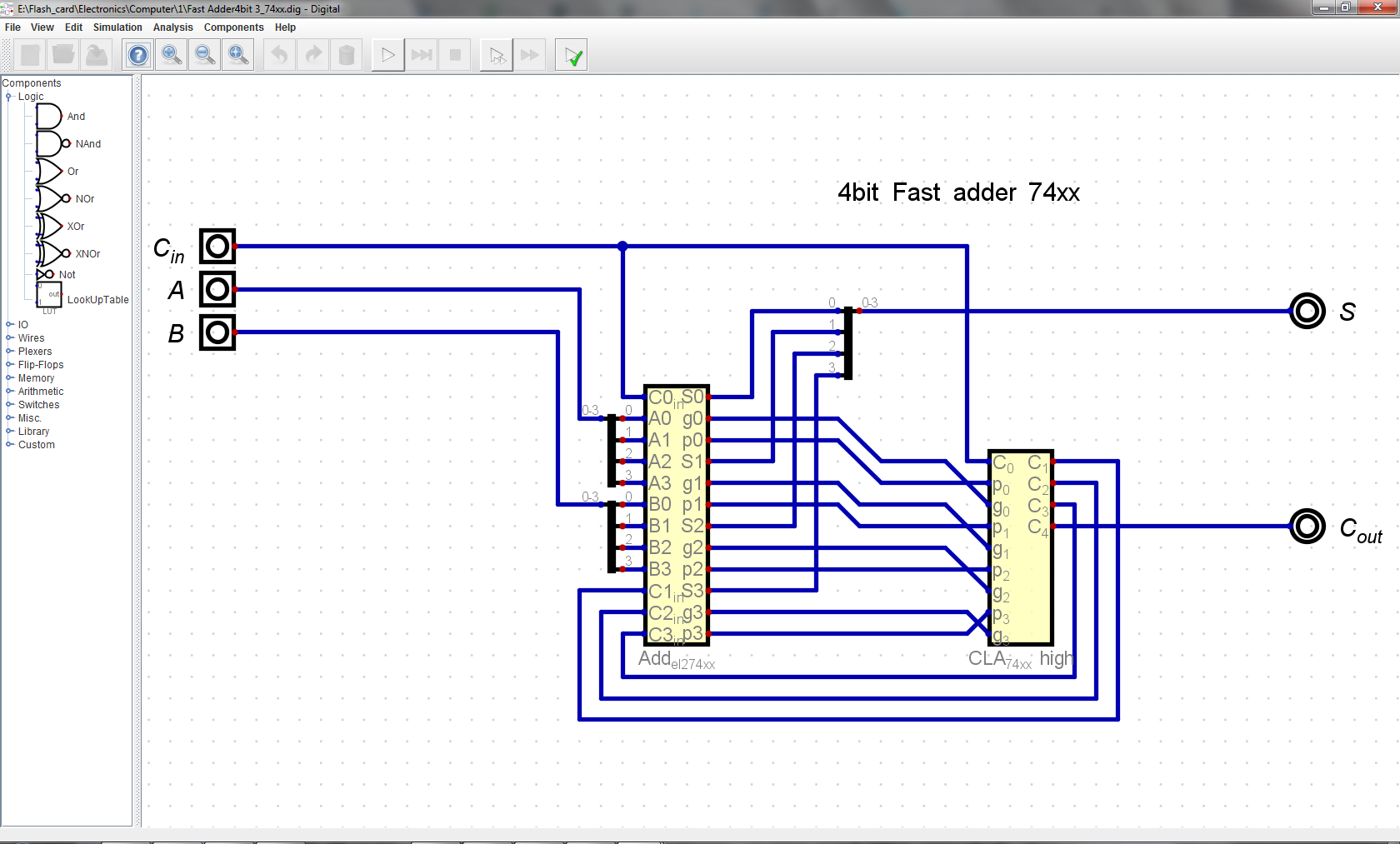
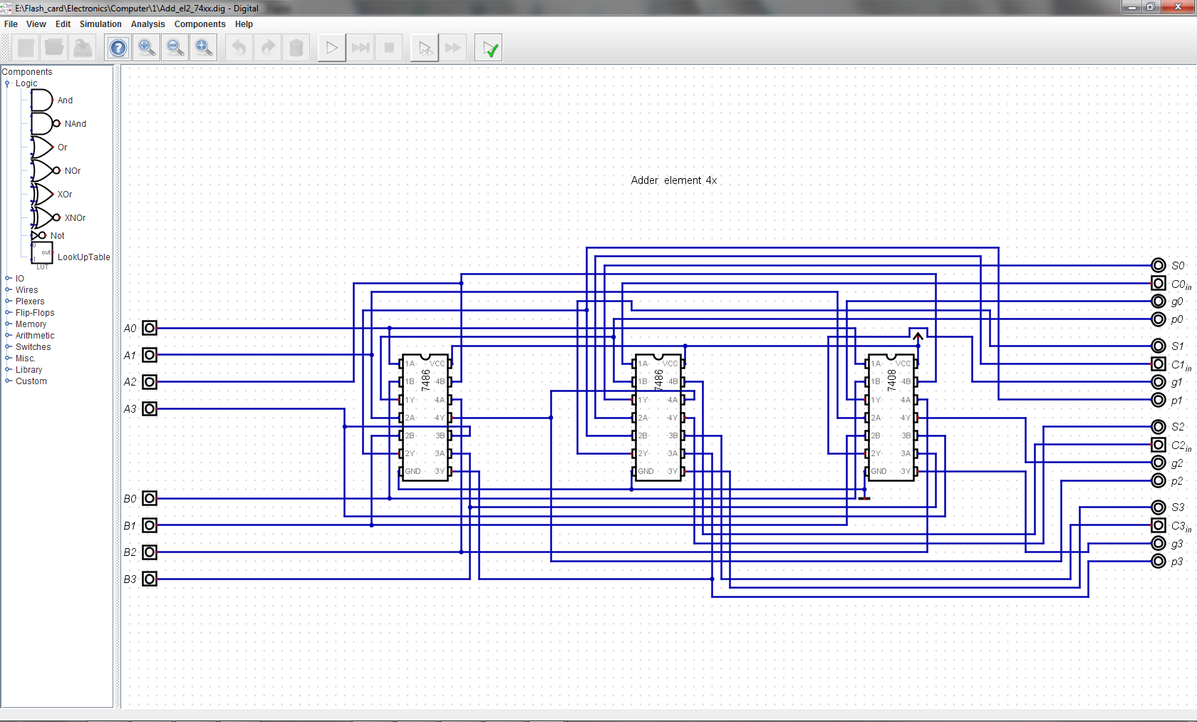
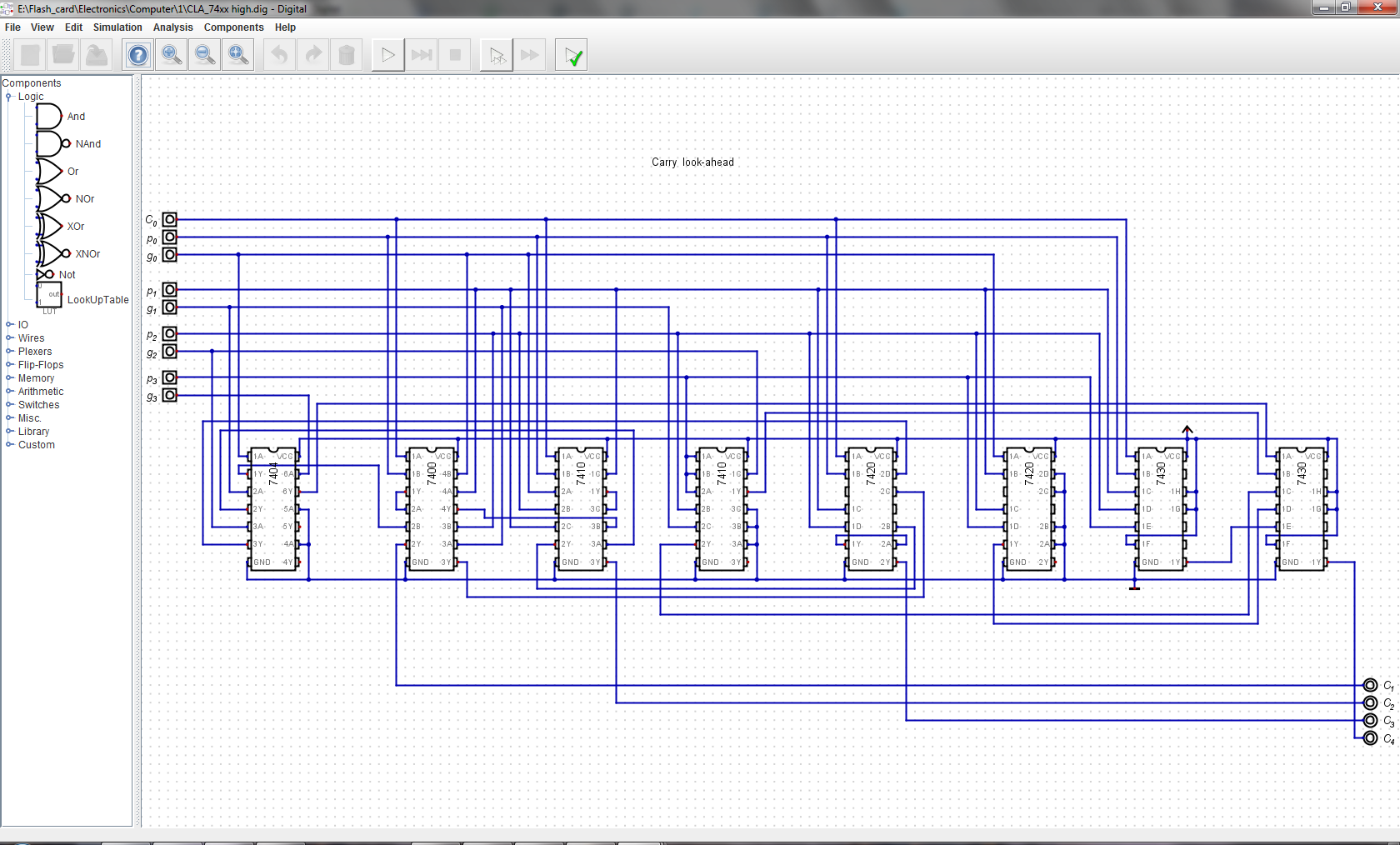
Fast adder takes in C_in, A_in and B, outputs S and C_out. It is comprised of four chained 4-bit fast adder units. Constructed from simple logic gates throughout, no fancy 74181/2/3 chips.
![]()
![]()
![]()
![]()
Logic unit also operates on A_in and B_in inputs bitwise, has three outputs. Essentially, it is compound XOR gate ( made from ANDs and NORs + inverters), so AND, OR and XOR are achieved in the same circuit.
![]()
The last stage is the big 8-to-1 16 bit mux, which is controlled by 3-bit F (as in Function) control line. It chooses which function result will be output from the ALU.
Here are these functions:
000 Zero -- no matter what inputs, all bits are set to '0' output
001 A shifted -- whatever comes from the Shifter unit (itself controlled by A, L/r and sh/RC lines) -- could be SHL, SHR, ASHR, ROLC, RORC
010 A -- A_in goes straight through to the output
011 ~A -- A_in gets inverted
100 ADD (A,B) -- result from adder, can be any of the ADD, SUB, ADDC, SUBC
101 AND (A,B)
110 OR (A,B)
111 XOR (A,B)
In total, this ALU is capable of 28 different operations, though in many cases some of the operations can give the same result.
-
At the beginning...
08/16/2018 at 07:47 • 0 commentsSo, a couple of years ago I've seen people over the internet making their own computers and CPUs from scratch at home, the kind of thing that average person would think is possible only in industrial setting by a team of experts. Since then this idea has infected my mind, and I started to learn electronics and digital circuits in my spare time, then bought soldering iron and small assortment of electronic components, and started to experiment.
A year ago I first started to think seriously about really building a cpu, then I thought that using individual transistors would be cool (I still think so, but it means A LOT of tedious work, with at least half of the circuits not working as designed at first). At that time I read several books about cpu design (But how do it know?, DIY Calculator, and others). Based on my new knowledge and estimating my limitations, I decided, that this computer should be based around 16-bit datapath, and to have 16-bit wide instructions. It also would have 16 bit memory (data and address), all for simplicity of implementation.
The instructions are not to be microcoded, but rather decoded from instruction word by combinational logic. 16 bit instructions are this width explicitly for ease of decoding. Longer instructions would be even easier, but it may increase component count and overall cost beyond what could be allotted to it.
Another feature is register file of 8 16-bit registers, so they are addressed by 3-bit addresses. They are to be operated as: A <-- ALUop(A,B). General architecture is Load/Store.
Well, after that I put this project on hold, and recently, some month ago I turned to it again. I made simulations in Digital for ALU and Register File first, and around that started to design the rest of the system. Right now I am implementing instructions for this simulated computer, and it already kind of works, with little program in machine language.
The instructions available now are:
ALU instructions -- the simplest decoder, because ALU instruction is almost the same as instruction word for hardware. There are quite a lot of different instructions, so the ALU can do many things with its operands, which could be one of the registers, two of the registers, or one of the registers and some 8-bit constant, which is encoded in instruction.
Short jumps (within 256-byte page) -- unconditional, and on condition of Carry, Negative, and Zero flags. Lower 8 bits of jump address are encoded in instruction itself.
Load from page -- can load a word into one of general purpose rgisters from within the current memory page (256 byte long), as the lower 8 bit of memory address is encoded into instruction.
Load immediate -- loads a word which is on the next address after instruction.
Here is screenshot of this "computer" simulation running a small program running in Digital digital logic simulator (only part is seen):
![]()
This is work in progress (in the beginning stage of it), so the layout is subject to great change.