-
1Flash transmitter LPC2148 with the transmitter code
The transmitter code has been provided in the files section.
Connect pin 0.9 (UART 1 - RX) to the data pin. Also make the appropriate Vdd and ground connections. The received signal is then repeatedly transmitted through 0.0 (UART0 - RX) to the data pin of FS1000A Transmitter. This is done so that the receiver does not pick up noise in between successive transmissions. The schematic of the transmitter side and our circuit can be seen as follows:
![]()
![]()
-
2Flash receiver LPC2148 with the receiver code
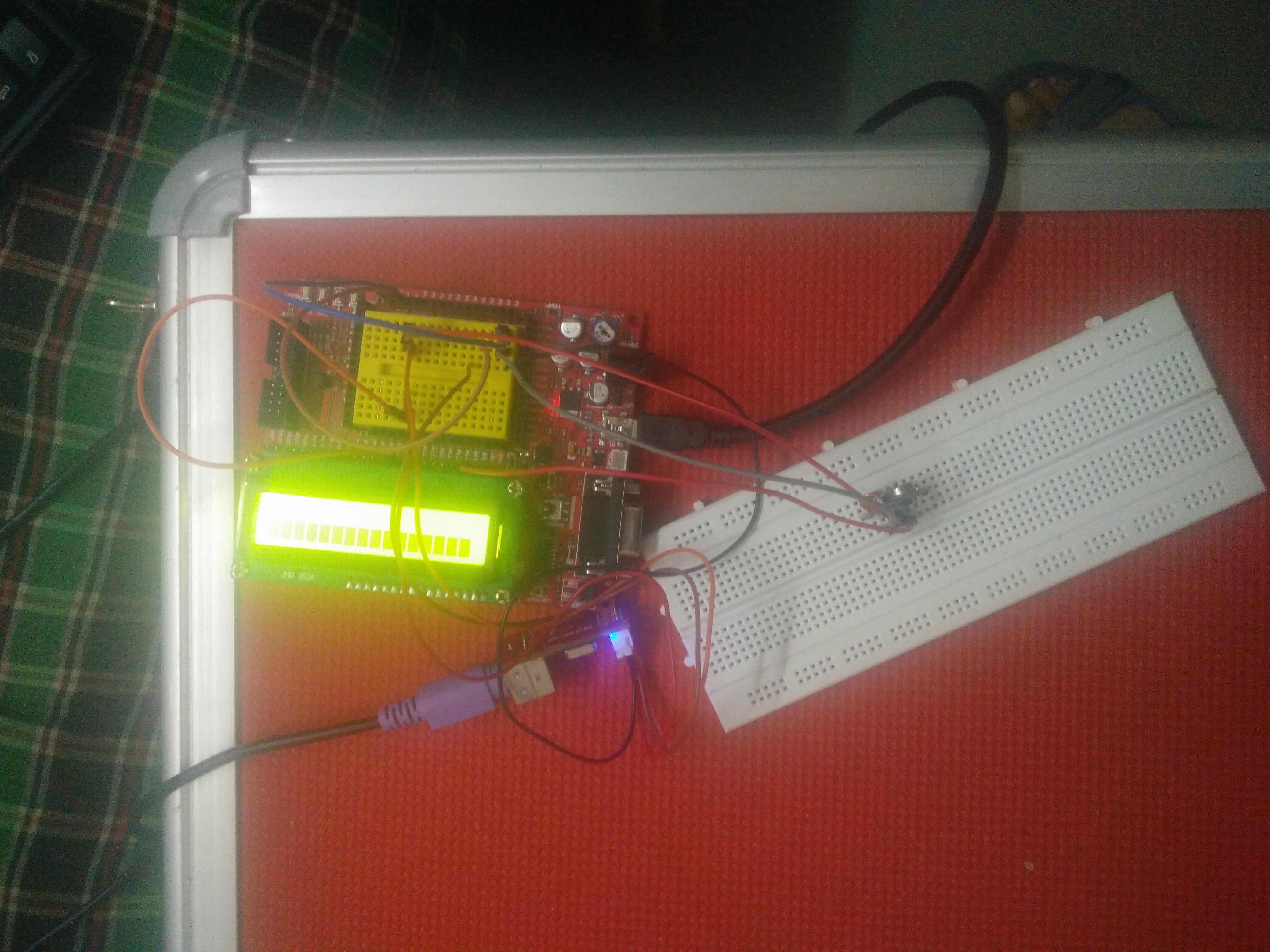
At the receiver end, we have 0.9 (UART1 -RX) connected to the data pin of FS1000A Receiver. This is then decoded (code is attached in one of the previous sections) using a look-up table. Support for more keys can be added. The LCD is also initialized to assist in debugging. The schematic and the circuit can be seen below:
![]()
-
3Receive output on a text editor
The receiver LPC is flashed with the receiver code, with the ISP jumper in place. After flashing, the ISP jumper is removed, and placed to connect the JTAG pins. Any value pressed in the PS/2 keyboard should ideally appear on the LCD screen. If it does not, then wait for some time for the receiver to perform gain adjustment. Now the received values must automatically write into any open text editor window.
An RF Adapter to Make a PS2 Keyboard Wireless
Using FS1000A to communicate between a PS2 keyboard and Host PC
 Abhinav S


Discussions
Become a Hackaday.io Member
Create an account to leave a comment. Already have an account? Log In.