0%
0%
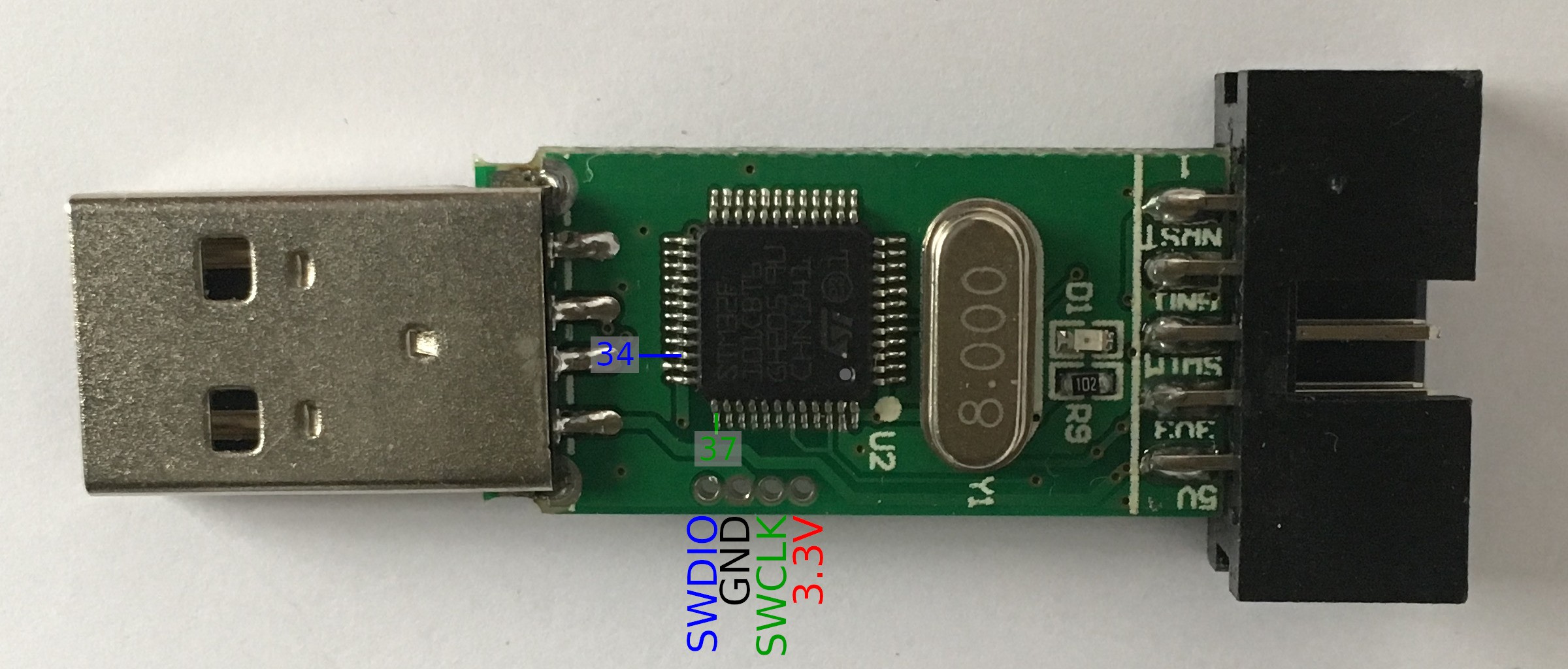
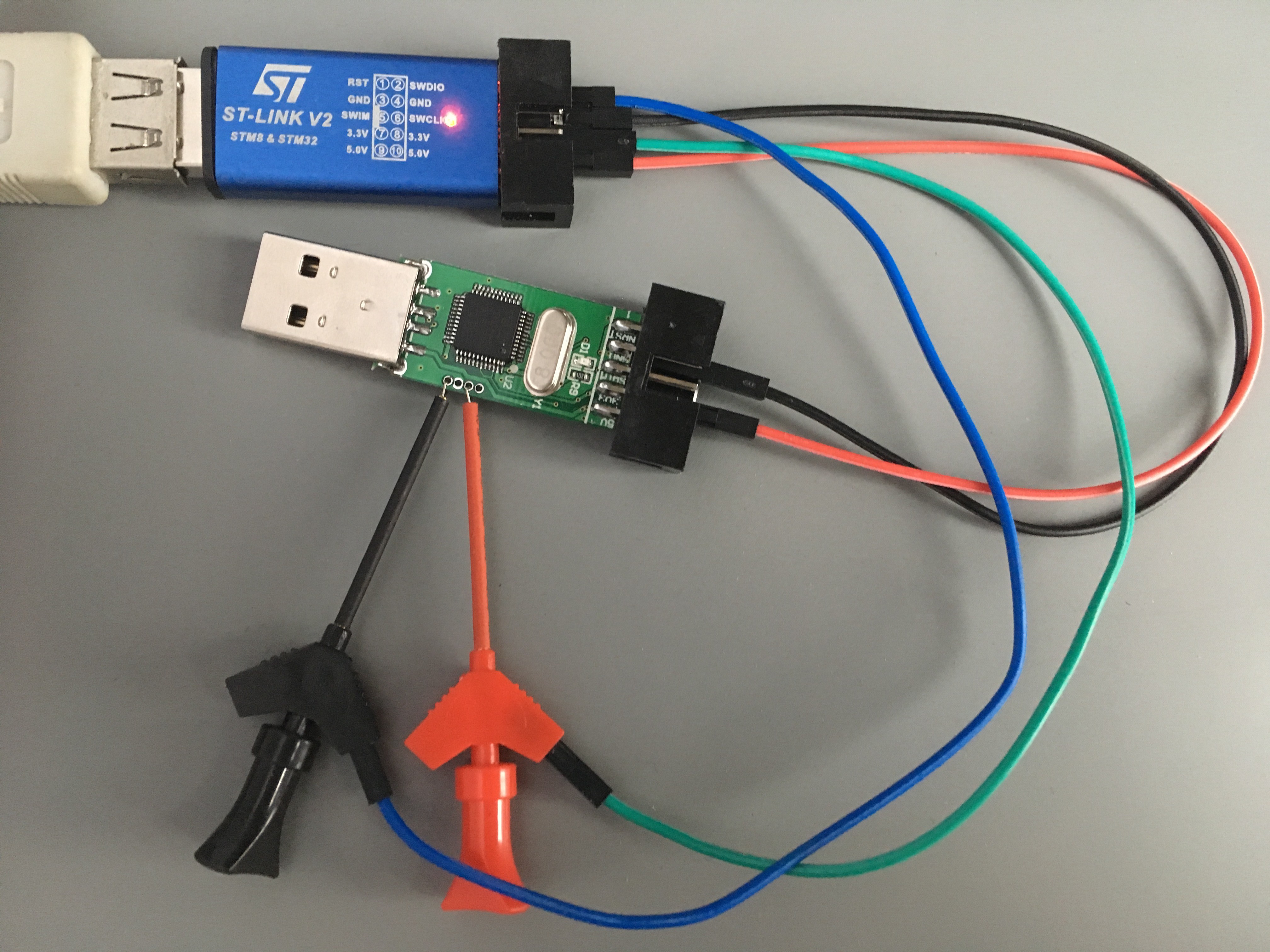
ST-Link clone repurposing
An ST-Link clone has a powerful MCU, nice enclosure and useful connectors to repurpose it for quite some projects.
 gertux
Become a Hackaday.io member
Already have an account? Log in.
Just one more thing
To make the experience fit your profile, pick a username and tell us what interests you.
Pick an awesome username
hackaday.io/
Your profile's URL: hackaday.io/username. Max 25 alphanumeric characters.
Pick a few interests
Projects that share your interests
People that share your interests


 Michele Perla

 benjaminaigner
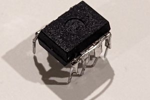
 Shranav Palakurthi
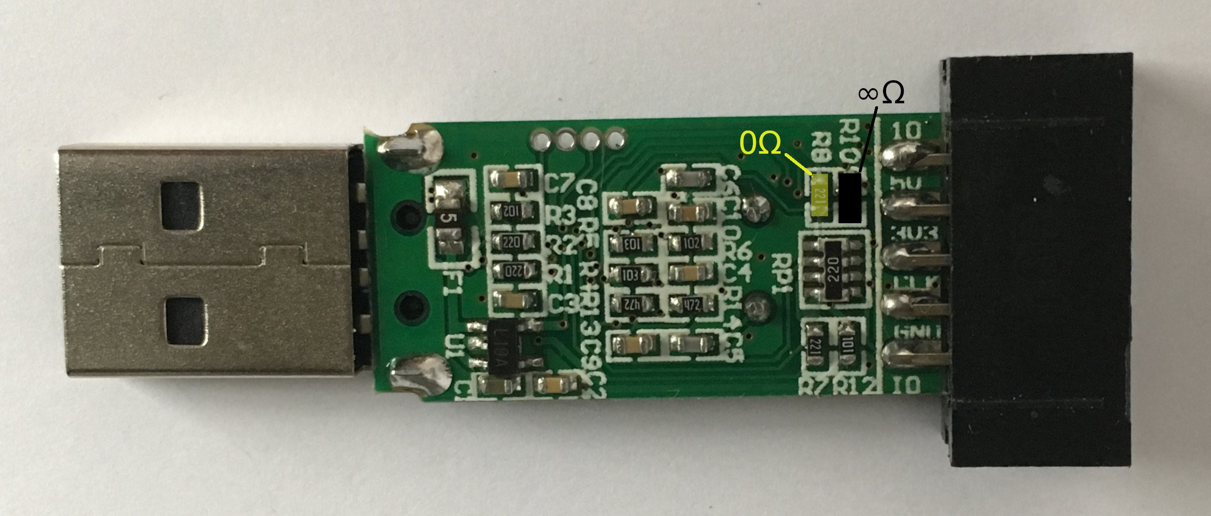
Well can access to ST link cpu but cant unlock it, so cant program it