2-Zons
-
No more loopy wires
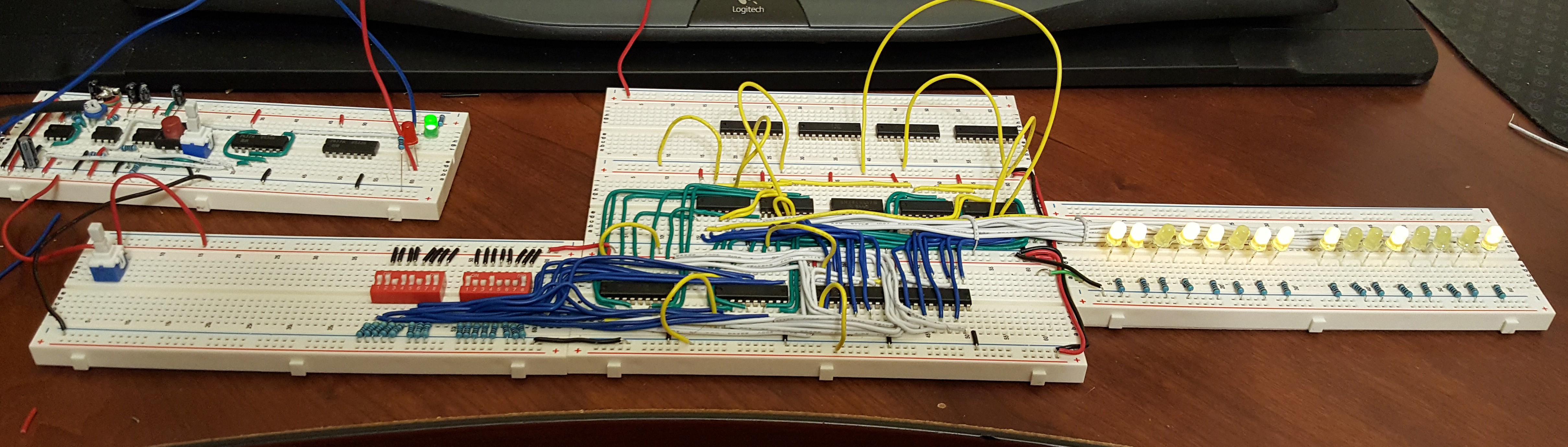
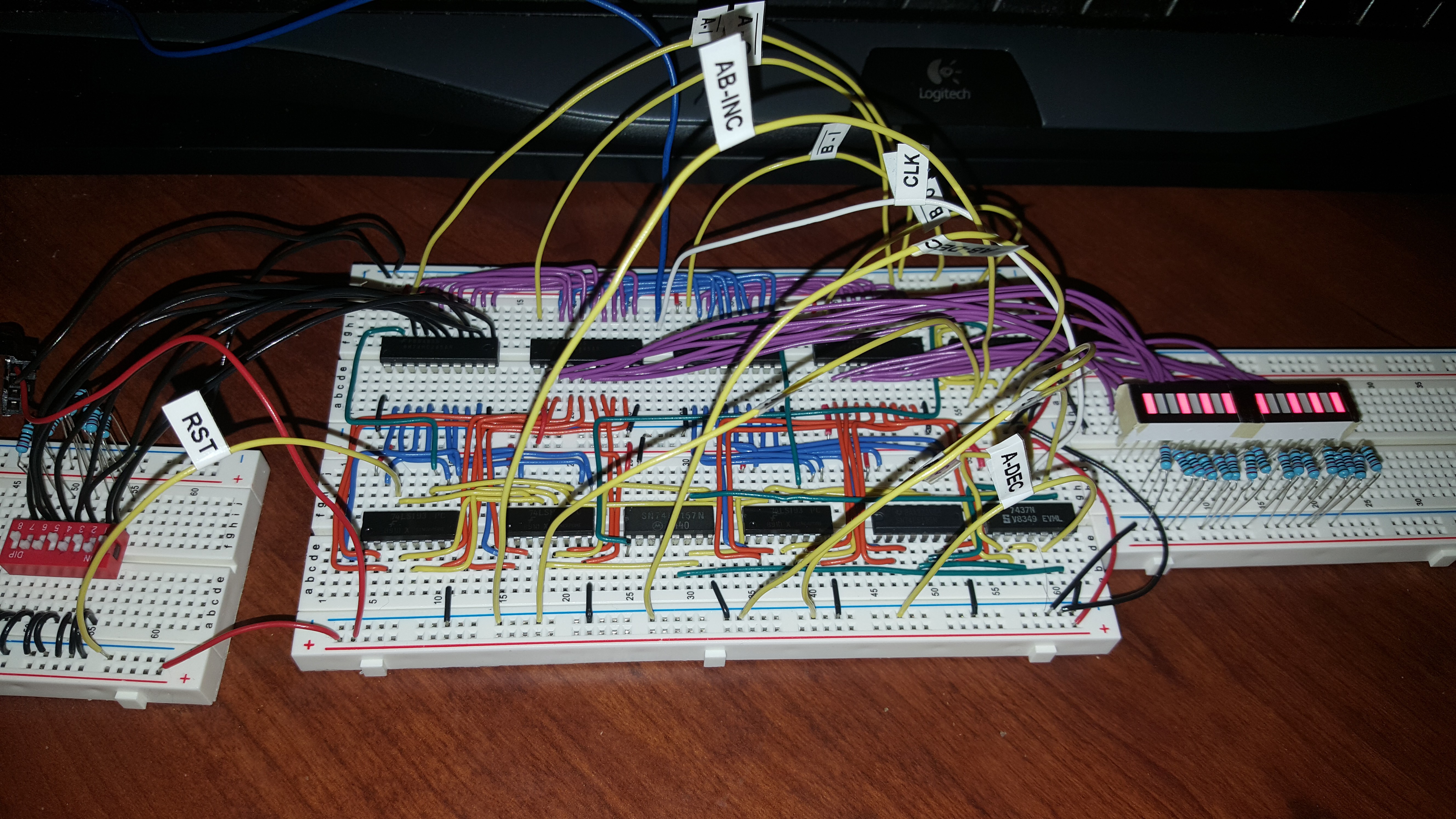
02/17/2019 at 20:47 • 4 comments![]() Finished routing all the control signals to a single board. Need to build a few more ribbon cables for the address bus, data bus connections and LED's. Looks much neater now. Modules completed thus far (from left to right in picture): RAM / ROM module, ALU, XY register, stack pointer, and AB register.
Finished routing all the control signals to a single board. Need to build a few more ribbon cables for the address bus, data bus connections and LED's. Looks much neater now. Modules completed thus far (from left to right in picture): RAM / ROM module, ALU, XY register, stack pointer, and AB register. -
Added RAM and ROM module
02/10/2019 at 04:24 • 2 comments![]()
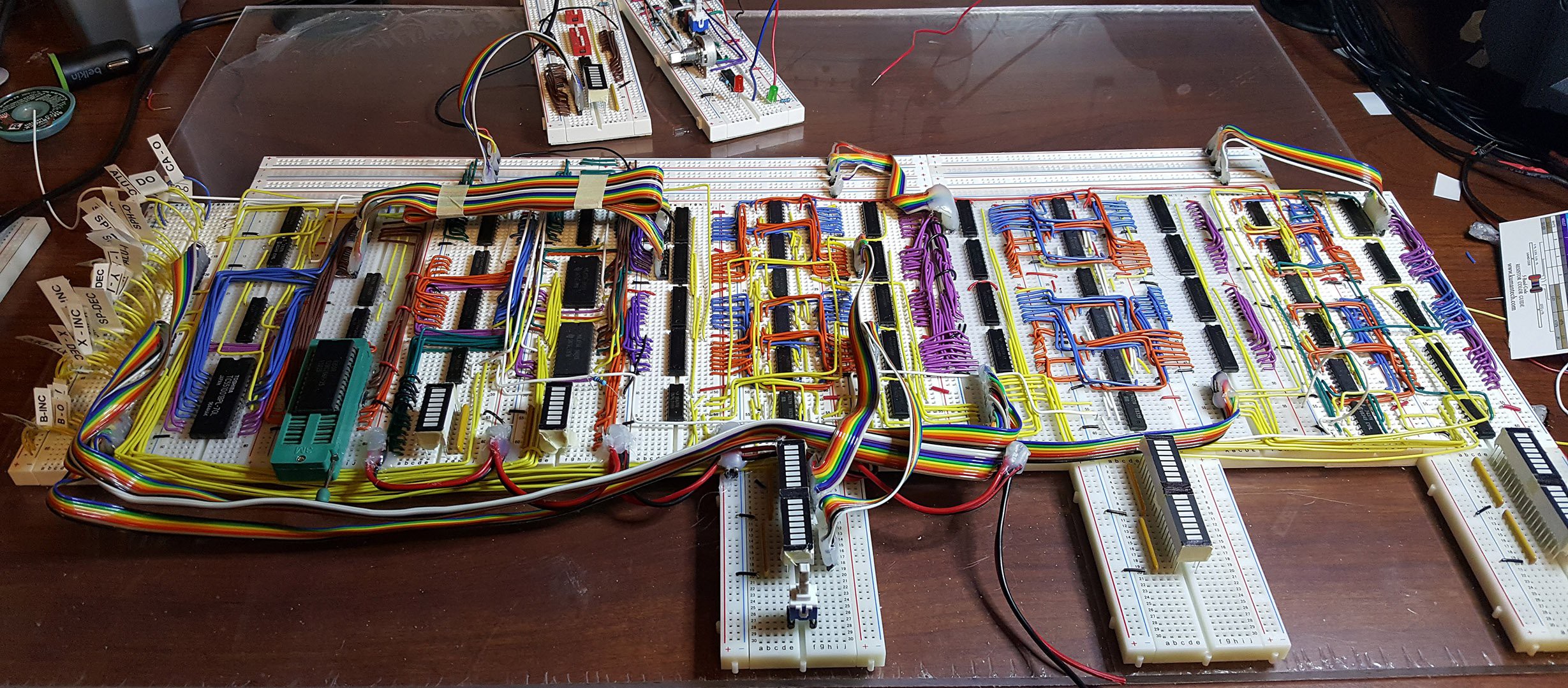
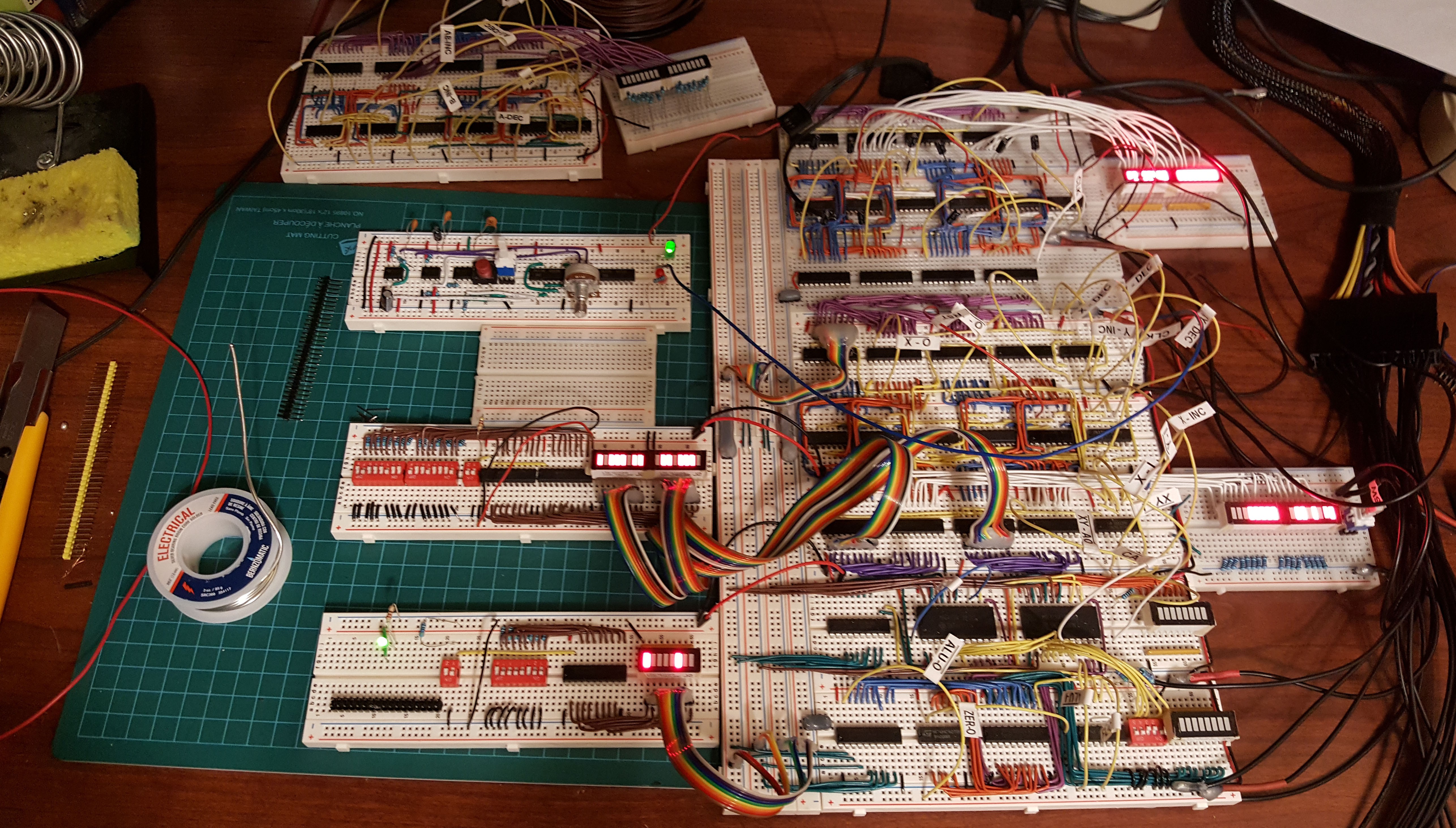
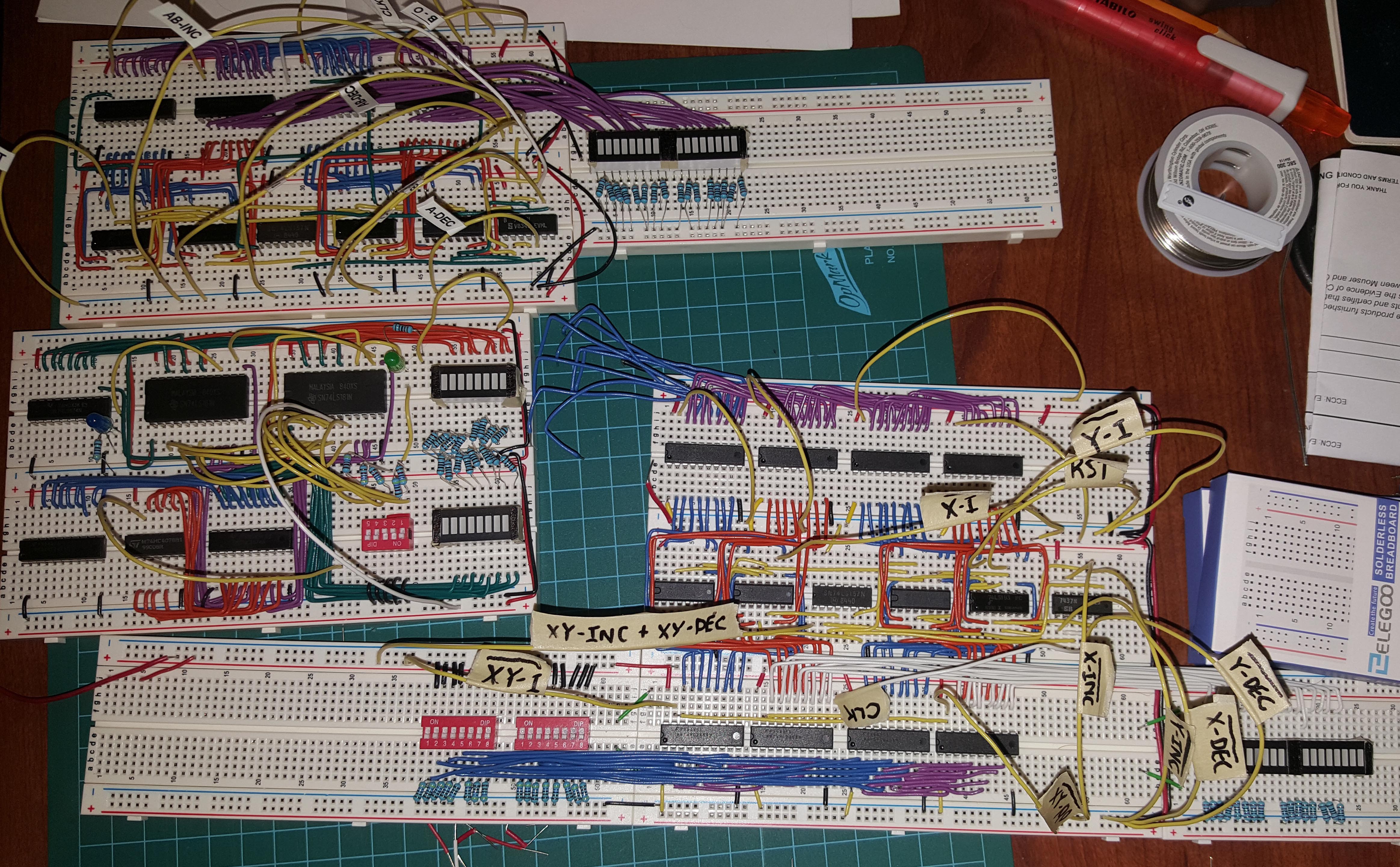
I'm back from my little vacation in Vegas and have been busy building. I bought a sheet of 1/4" acrylic to mount all the boards together. I was tired of trying to clip them together with wires or headers. It's working nicely. I wanted to start running all my control lines into their positions so I can get rid of all those big loopy wires. I couldn't do that until I had a place for them all to go (the empty board at the bottom). I have room for another column of breadboards on the left side of the data bus.
I finished the RAM / ROM module and tested it. I used a ZIF socket for the 32K ROM chip to make reprogramming quick. I have more of them for the microcode ROM's. The address bus is removed in the picture as well as the data bus connections to the RAM ROM module. The RAM / ROM module is technically "external" to the CPU and my DI control line would be the R/W output. The DI control line would control the tri-state buffers between the internal and external data bus.
-
Connectors and Glue (the sticky kind)
01/25/2019 at 23:03 • 1 comment![]()
I've been working on cleaning things up and building connectors to make things easier. I'm using headers and ribbon cable to replace a lot of the bundles of lose wires. I've also improved my power situation by using a 850W ATX power supply. 850 watts is total overkill but it's what I had lying around. I also finished building the stack pointer (it's on the top right) I've also built some bridges to hold the breadboards together and connect them using headers and hot glue. I've been using a lot of hot glue, truly magical stuff. I'm going on a trip for a few days so I will be taking a break from construction.
-
Combining Modules
01/20/2019 at 03:51 • 3 comments![]()
I've been working on combining the modules I have so far. It's been I little trickier than I'd hoped but It's coming along. I built a temporary data and address bus driver with LED readout. In my initial testing I just had the dip switches connected to the data inputs of the modules. This wouldn't let me test the modules output to the bus. So by separating the dip switches with their own bus driver I can now test what the modules put out on the data bus. I did the same with the address bus. I'w worried that all these dip switches are going to draw too much current though. I think if I make a front panel for the system I will use toggle switches that simply switch between VCC and GND.
On another note. Upverter sent me an email. They chose my project for a case study. They want to help me get it manufactured (PCB and components).
-
Status Register
01/16/2019 at 22:48 • 0 comments![]()
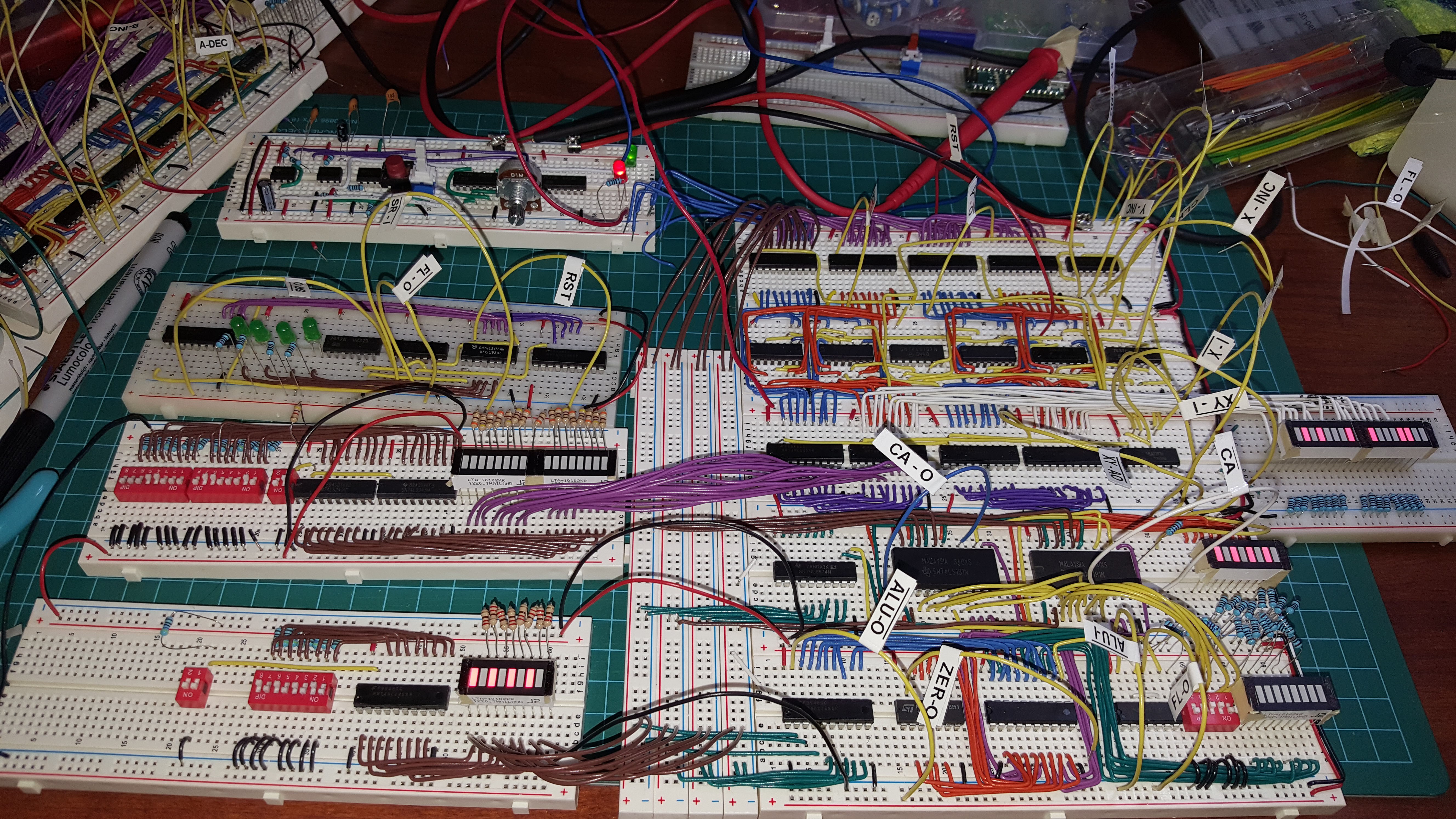
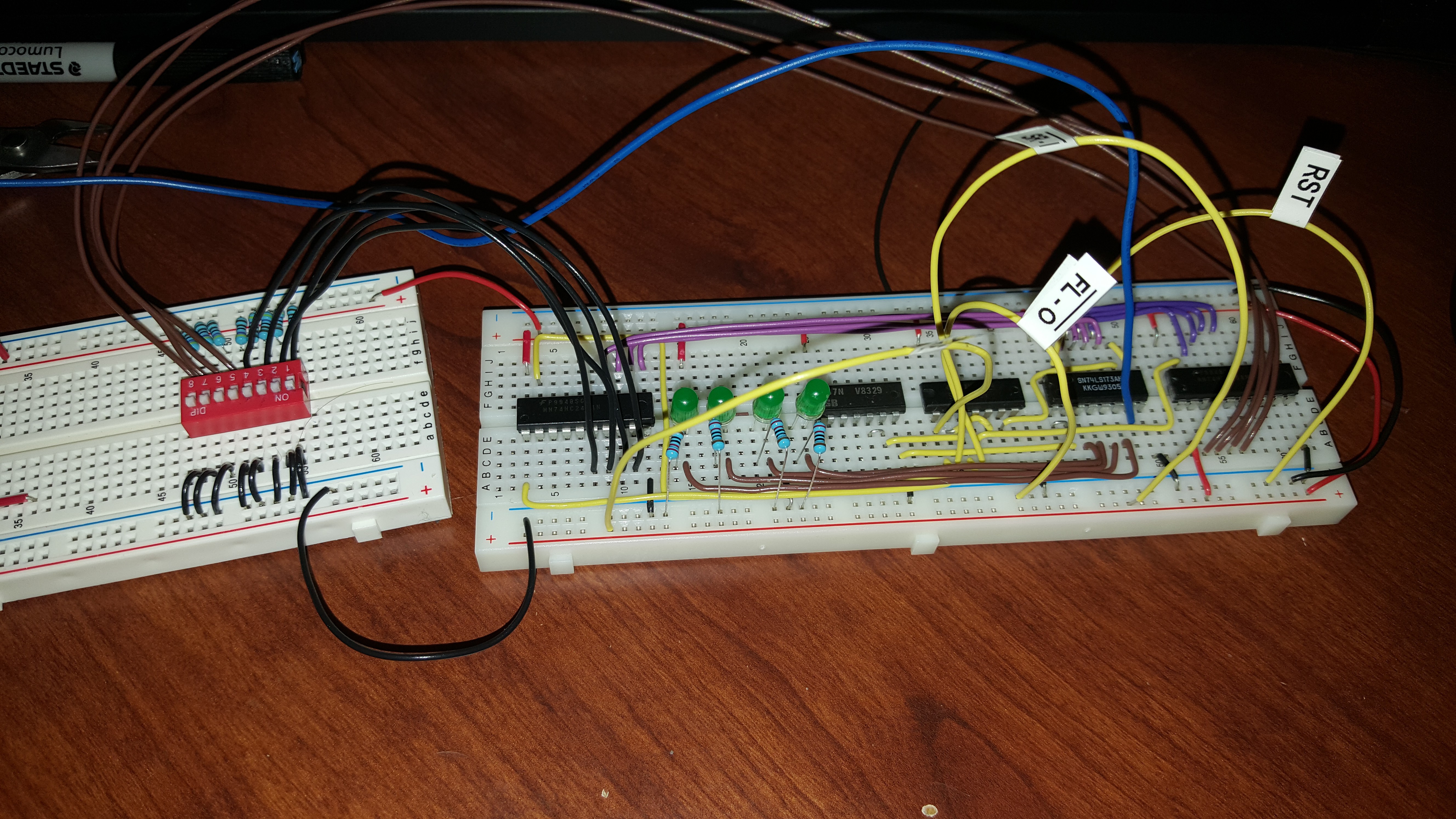
Finished this last night. This was more difficult than I expected. It's only a 4 bit register but it took quite a bit of translation from logisim to reality, trying to keep the chip count low and minimize unnecessary gate delays. My satus register (SR) has 4 flags: Equal EQ, negative NE, zero ZE, and carry CA. SR is set by the ALU during any ALU operation. It can also be set by loading a value from the data bus. The CA flag will affect subtraction or addition in the ALU. All 4 are used by the instruction decoder for conditional jumps. The SR can also be sent out to the data bus for saving it on the stack or for logical functions in the ALU. I was able to get by using only two 2 way bus driver IC's. One for both in from, and out to the data bus, and the other for buffering the flag outputs of the ALU. This is what made it tricky to make sure that the internal bus in the SR would never have more than one source based on the control signals: FL-O, Flags out to data bus; FL-I, flags in from data bus; and FL-O, store flags from ALU (an operation is taking place).
In the block diagram and in logisim SR is an 8 bit register, the first 4 bits being the instruction step counter. Since each 4 bits needs it's own IC (a counter and a D-flip flop), and they work completely independently of each other I will move the step counter to the same location as the instruction decoder. Keep the wire runs shorter. The step counter is never loaded from or sent to the data bus.
I've got enough modules completed to start fitting them together. Which is what I'm working on now
-
AB Register
01/15/2019 at 21:14 • 1 comment![]()
Finished the AB register. It's the same as the XY register minus 16 bit in and out to address bus. I'm getting much better at the wiring. For previous modules I would wire up just enough that I could test it, and then add a bit at a time testing as I went. This time I wired up the entire thing before testing, and only had one mistake when I fired it up (two bits crossed over on A). It was a quick to spot and quick to fix. My productivity should go up now. I've also received all of my orders so I have everything I need to complete the entire system. I dug up my label maker to tag the control lines.
![]() I'm getting enough modules complete to start wiring them all together. I can better judge now how many boards it will take for the whole system. I wish I could buy the power rails separately. I will be needing quite a few for data and address bus.
I'm getting enough modules complete to start wiring them all together. I can better judge now how many boards it will take for the whole system. I wish I could buy the power rails separately. I will be needing quite a few for data and address bus. -
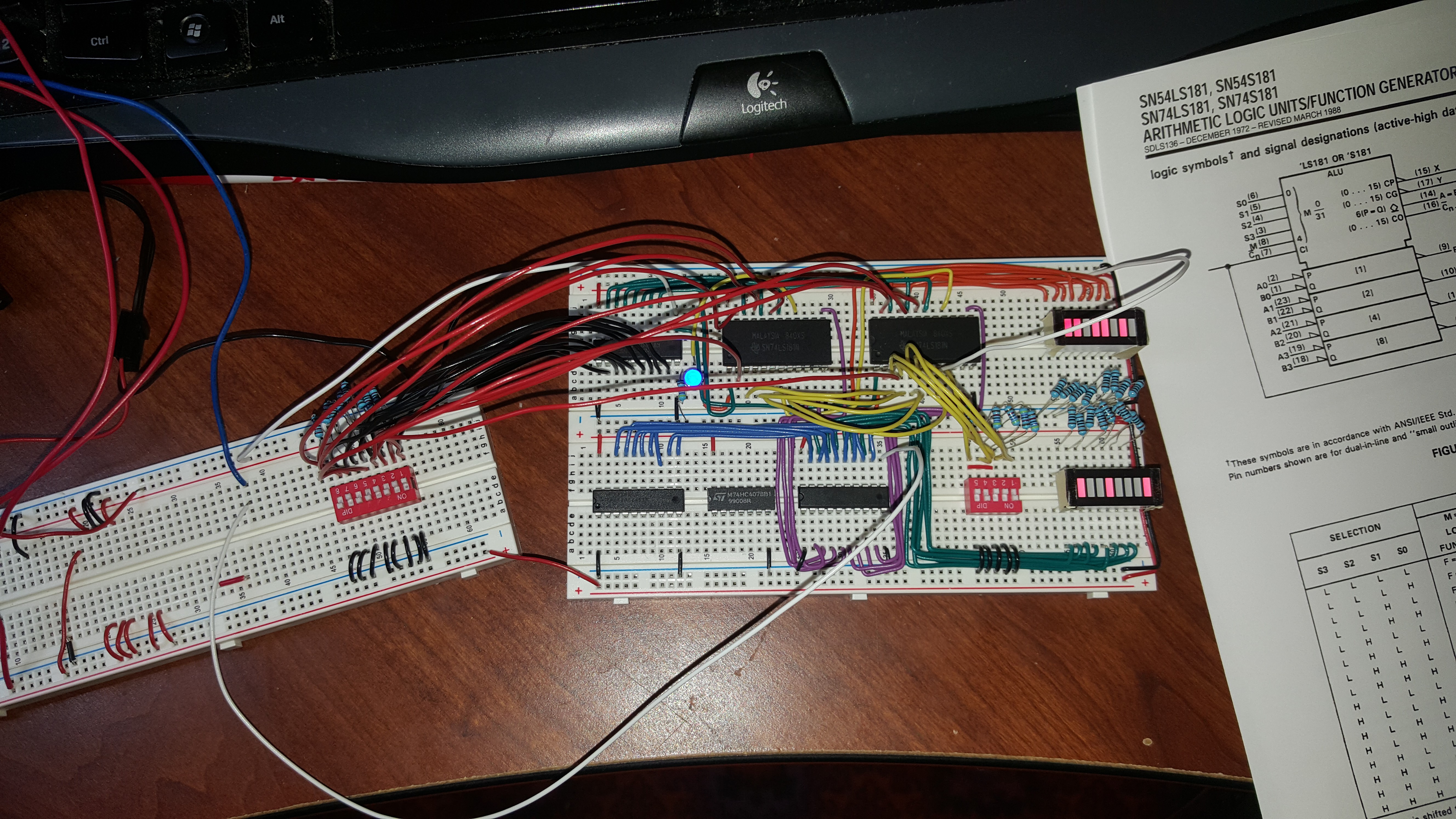
ALU
01/14/2019 at 02:36 • 1 comment![]()
ALU is mostly complete and working. Using 2 x LS181's. Top right LED's show contents of input register tied to input B on 181's. Databus (Dipswitches) tied to input A. Blue LED is carry not. Bottom Right LED's show contents of output register. Showing A XOR B. All loopy wires are temporary for testing, as well as the 5 dipswitches on the board, they will be control signals when hooked up to the bus. Only need to implement zero, negative, and equal flags. I hope I can use the A=B output on the 181's and'ed but when I tested it in logisim it didn't work properly. I haven't tested on this setup yet.
-
Completed and Rebuilt XY Register
01/12/2019 at 04:32 • 0 comments
I started over and completely rebuilt the XY register. I was having trouble with the bus drivers. I switched to 74HC245's from 74ACT241N's. The 241's were actually dual 4 bit buffers each with their own enable line (one active hi and one active lo). The enable lines couldn't be tied together and each 4 bits was output on opposite sides of the chip which made wiring really messy. I also got new wire delivered which is the same guage (22AWG) but has a thinner insulator and is much nicer to work with. I've tested out all the functions and they all work: X inc and dec; Y inc and dec; XY inc and dec; load XY from address bus; load X or Y from data bus; push X or Y to databus; push XY to address bus; and reset. Only thing left is some control signal logic which I am missing some OR gates to complete. I neglected to order them earlier. I think I'll build the ALU next.
-
XY Register
01/08/2019 at 04:37 • 4 comments![]()
Working on the XY register. This is the register with the most control signals and features. Separate hi, lo byte, and word increment and decrement. Hi or lo byte in from or out to databus. Word in from or out to Address bus (Address bus is used for 16 bit register to register transfers). The address bus side of in and out is finished and tested. Need to wire data bus in and out and lo byte to hi byte up down logic. I've already used over 40' of wire just for this one register. I'm going to need a lot more. The yellow loops are control signals tied hi or lo for testing. Dip switches are acting as the address bus.
-
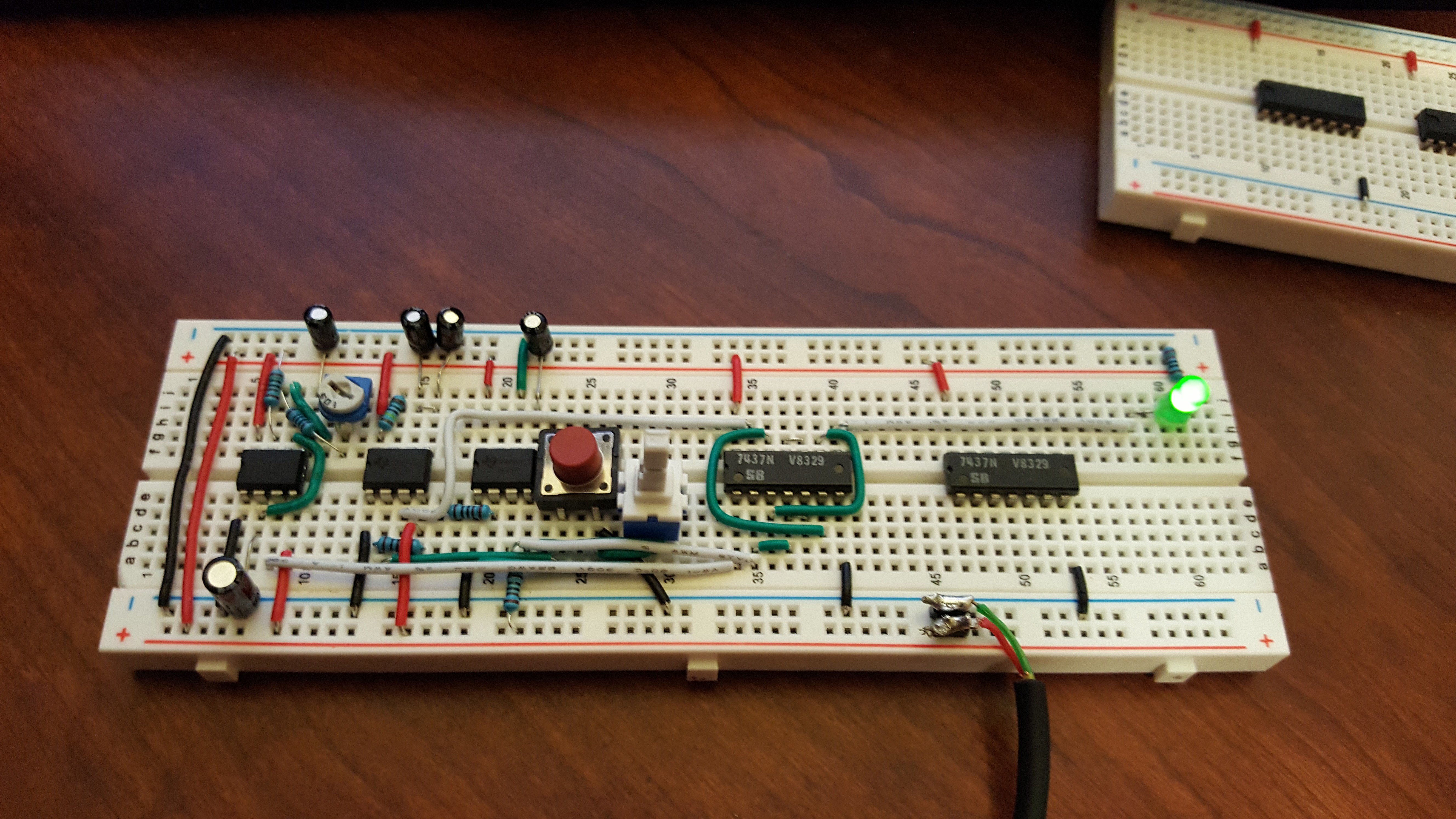
Construction has started
01/06/2019 at 00:18 • 3 comments![]()
Finally received the delivery I was waiting for to start building something. This is the clock circuit. It's pretty much an exact copy of Ben Eater's 8 bit computer clock. Starting from the left: A 555 circuit to generate and adjustable square wave clock that can run as slow as 0.5 Hz. Second, another 555 circuit to debounce a pulse that will be fed into the output logic for single stepping. Third, a final 555 circuit to debounce the enable circuit that feeds into the output logic to select from the single step or clock. Red button is single step pulse, beside the toggle for the select. Next are two quad nand 7437 for the output logic. Second chip is not used yet. Will be used to generate inverse clock, and halt for DMA.
No need to comment on the crappy soldering job on my power input.
8 Bit Breadboard CPU
A home-brew 8 bit Microprocessor built on a breadboard 64K Address Space, IRQ, and DMA 16 Bit Stack Pointer, 4 8 bit Registers or 2 16 bit
 Finished routing all the control signals to a single board. Need to build a few more ribbon cables for the address bus, data bus connections and LED's. Looks much neater now. Modules completed thus far (from left to right in picture): RAM / ROM module, ALU, XY register, stack pointer, and AB register.
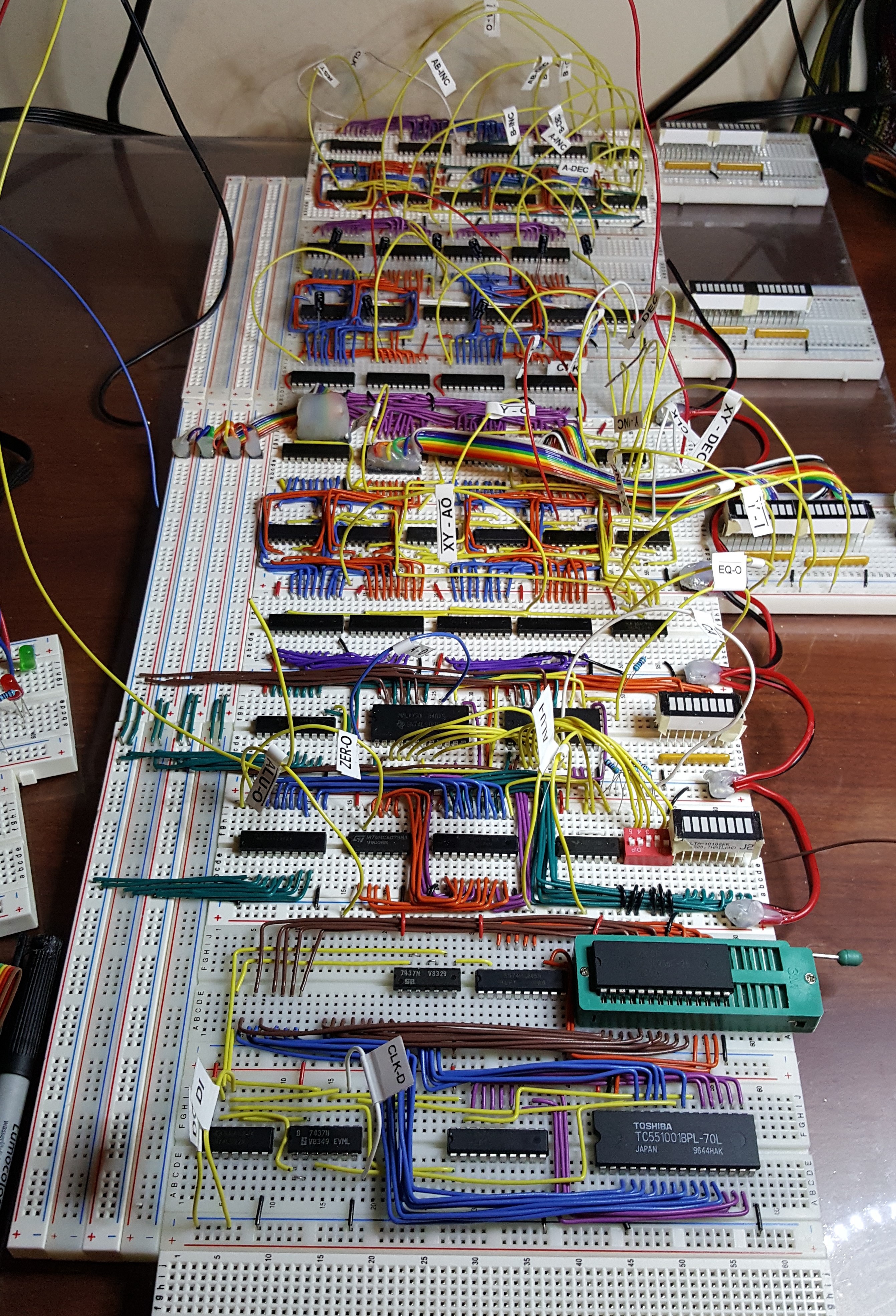
 I'm getting enough modules complete to start wiring them all together. I can better judge now how many boards it will take for the whole system. I wish I could buy the power rails separately. I will be needing quite a few for data and address bus.